Importance of Electronic Correlation in the Intermetallic Half-Heusler Compounds
Abstract
Low temperature scanning tunneling spectroscopy of HfNiSn shows a zero bias anomaly around the Fermi level. This local density of states with a fractional power law shape is well known to be a consequence of electronic correlations. For comparison, we have also measured the tunneling conductances of other half-Heusler compounds with 18 valence electrons. ZrNiPb shows a metal-like local density of states, whereas ZrCoSb and NbFeSb show a linear and anomaly. One interpretation of these anomalies is that a correlation gap is opening in these compounds. By analyzing the magnetoresistance of HfNiSn, we demonstrate that at low temperatures, electron-electron scattering dominates. The temperature dependence of the conductivity confirms that the electronic correlations are a bulk rather than a surface property.
- PACS numbers
-
May be entered using the
\pacs{#1}command.
pacs:
Valid PACS appear hereI INTRODUCTION
Recently, there has been renewed interest in more efficient thermoelectric materials because of the worldwide demand for sustainable energy sources. One such class of candidates are the half-Heusler compounds with 18 valence electrons. Among them, the MNiSn (M = Ti, Zr or Hf) compounds are narrow gap semiconductors with a gap size of 100- Yu et al. (2010); Xie et al. (2012). The narrow gap leads to a moderate electrical resistivity and a large Seebeck coefficient. This combination leads to a high , the figure of merit used to evaluate thermoelectric efficiency Yu et al. (2010); Wang et al. (2010); Xie et al. (2012). , where is the Seebeck coefficient, is the electronic resistivity, is the thermal conductivity and is the absolute temperature. Intensive efforts have been made to improve the ZT of MNiSn compounds. Because MNiSn compounds are n-type materials, all of the three sites, M, Ni and Sn, can be doped by donors to reduce the electronic resistivity Chen and Ren (2013); Hohl et al. (1999); Uher et al. (1999). Grain size and grain boundaries can also be engineered to achieve a better Seebeck coefficient Bhardwaj et al. (2012); Makongo et al. (2011). However, these attempts can be facilitated by a better understanding of the electronic structure near the Fermi level.
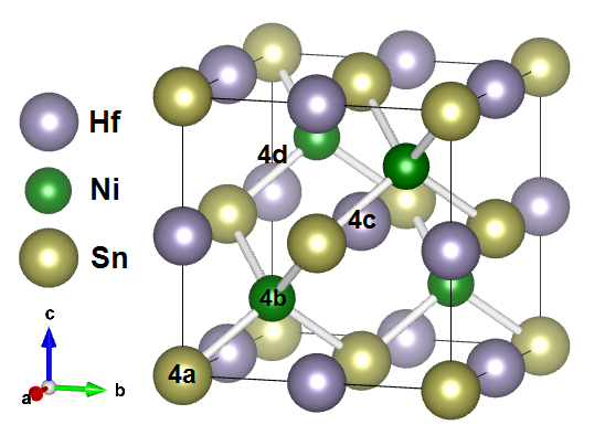
Half-Heusler compounds have the MgAgAs-type crystal structure which belongs to the F-43m space group. The crystal structure is shown in Fig. 1(a). It is comprised of four interpenetrating face-centered cubic sublattices. Two sublattices are occupied by transition metals. The third is occupied by a main group element and the fourth is occupied by vacancies. The vacancy sublattice distinguishes half-Heusler compounds from their full-Heusler counterparts as it induces a gap in the electronic structure. The intrinsic disorder observed in many half-Heusler compounds Aliev et al. (1989); Berche and Jund (2018); Xie et al. (2012) is known to be donors or acceptors that can generate in-gap states Berche and Jund (2018); Tang et al. (2018); Tian et al. (2018). Annealing can reduce the concentration of this disorder and transform the compounds from a metal to an insulator Aliev et al. (1989). Close to the metal-to-insulator transition, disorder breaks down momentum conservation and electronic screening becomes inefficient. Therefore, a strong electronic correlation is expected.
In this paper, we present scanning tunneling spectroscopy (STS) of four half-Heusler compounds. Except for ZrNiPb which has a metal-like local density of states (LDOS), the other compounds have different power law zero bias anomalies (ZBA) near the Fermi level, around which narrow but hard gaps should be expected. These anomalies are characteristic LDOS of a disorder induced metal-to-insulator transition (MIT) McMillan and Mochel (1980); Raychaudhuri et al. (1995). Details are discussed in Section \@slowromancapiii@.A. These giant anomalies in the one-electron local density of states play an important role in determining the electronic and thermal properties of these compounds. Ab-initio approaches generally fail to predict their existence Colinet et al. (2014); Berche and Jund (2018) and therefore, the subsequent conclusions from these approaches are unreliable. These anomalies also make it difficult to interpret the results of doping experiments because, instead of only shifting the chemical potential, doping also leads to the evolution of the anomaly Hertel et al. (1983); Lee et al. (1999). In Section \@slowromancapiii@.B and \@slowromancapiii@.C, the magnetoresistance and the temperature dependence of conductivity of HfNiSn are analyzed to provide more evidence for a strong electronic correlation in the material.
II EXPERIMENTAL DETAILS
The HfNiSn samples are flux-grown single crystals provided by our collaborator Dr. Lucia Steinke Steinke et al. (2018), who also provided the resistivity and magnetoresistance data. Details of sample growth and measurement of properties are described in Steinke et al. (2018). The ZrNiPb, ZrCoSb and NbFeSb samples are polycrystals provided by our collaborator Dr. Fei Tian of Dr. Zhifeng Ren’s group Chen and Ren (2013). Tunneling conductances are measured with a low temperature scanning tunneling microscope (STM) located in a 3He cryostat. Atomic resolution images of graphite and self-assembled dodecanethiol monolayer on an atomically flat gold surface have been obtained with this STM. Mechanically cut Platinum-Iridium tips are used. In order to get reproducible tunneling conductance and because of a lack of in-situ tip treatment device, tips are annealed in a Bunsen flame Libioulle et al. (1995). Using the same kind of tip, no ZBA is observed in the tunneling conductance of gold down to . Samples are cleaved right before experiments to expose fresh surfaces. Differential conductances are measured by a standard lock-in technique with a 0.5 mV modulation.
III RESULTS AND DISCUSSION
III.1 Local density of states
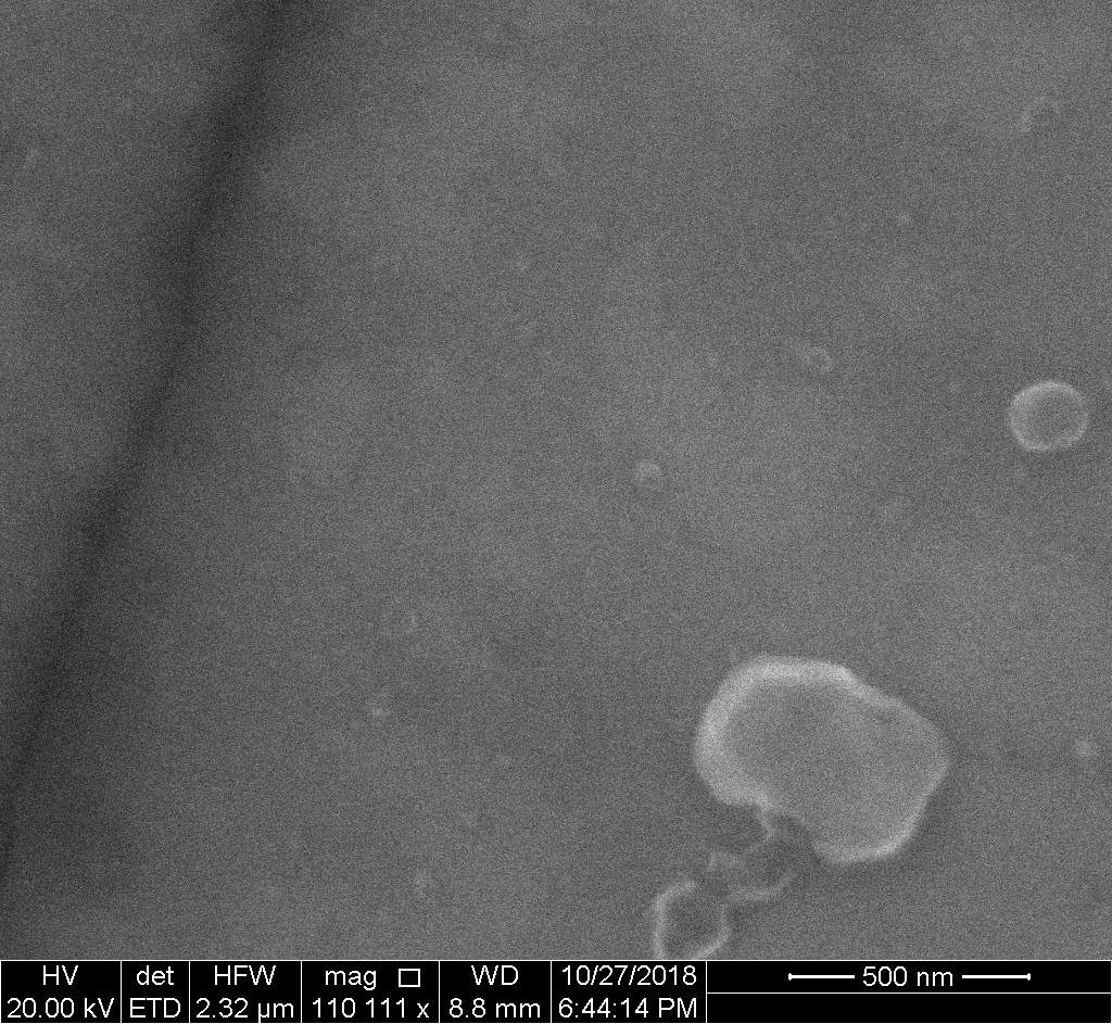
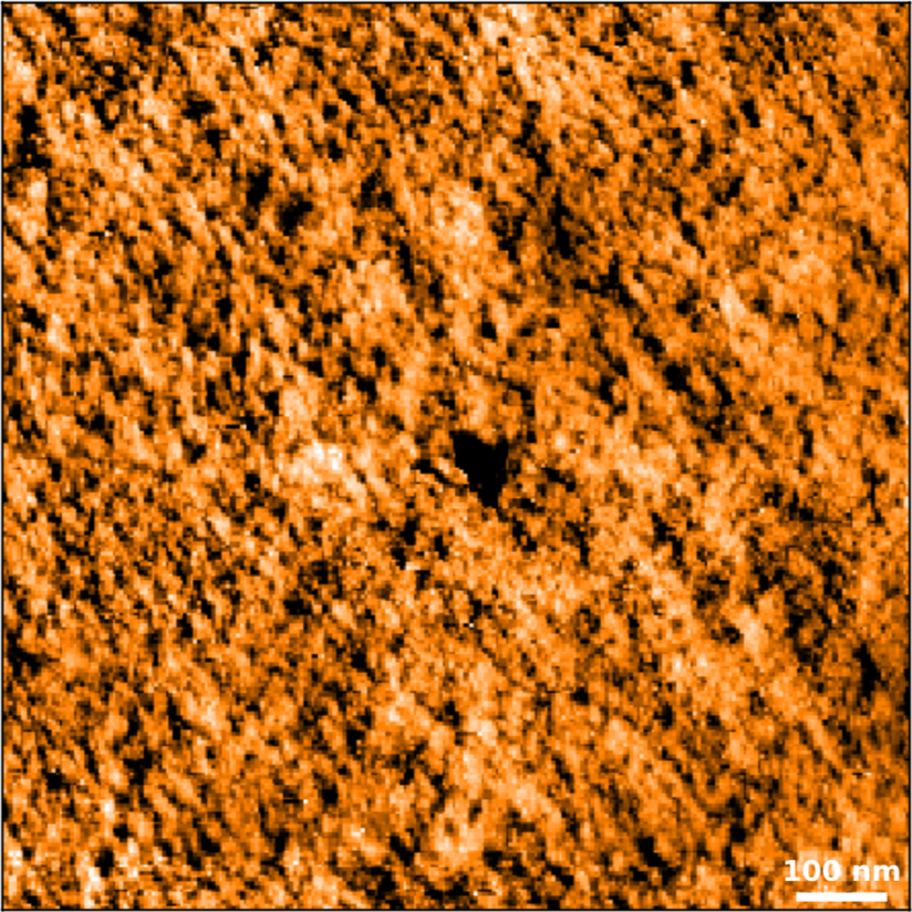
Figure. 1(b, c) show a comparison of a scanning electron microscope (SEM) and an STM image of a freshly cleaved HfNiSn surface. Although the STM reveals structures beyond the resolution of the SEM, the rough surface makes it difficult to achieve atomic resolution on these materials. Such a cratered surface is expected because of the vacancy lattice and the intrinsic disorder.
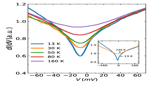
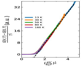
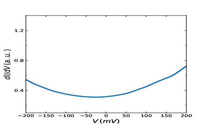
The tunneling conductances of two HfNiSn samples are more systematically studied. One shows a ZBA, common in disordered conductors with electronic correlation. The other shows a ZBA. The tunneling conductances of the latter at different temperatures are plotted in Fig. 2(a). All the minima occur at instead of at the Fermi level. The inset shows the conductances measured at and over a larger bias range, from which the shape is clear. Although the tunneling conductance does vary slightly across the surface, the dependence on voltage remains the same. Figure 2(b) plots versus , where is the tunneling conductance, and is the bias voltage. The straight dashed line corresponds to a dependence. Curves at different temperatures collapse to a universal one that is expected from the finite temperature density of states (DOS) calculated by Altshuler and Aronov Altshuler and Aronov (1985).
Tunneling conductance of nominal semiconductors can be sensitive to surface defects. But the conductivity discussed in Section \@slowromancapiii@.C supports that it is the bulk rather than surface electrons that are correlated. For films thinner than tens of nanometers, the conductivity should be proportional to Imry and Ovadyahu (1982a); Altshuler and Aronov (1985), whereas the corrugation of the rough HfNiSn surface is around from the STM topographic image. The dependence of magnetoresistance at high fields also demonstrates that the transport is 3 dimensional Imry and Ovadyahu (1982b).
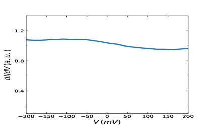
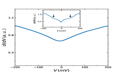
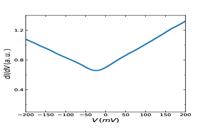
We further measured the tunneling conductances of other half-Heusler compounds, ZrNiPb, ZrCoSb and ZrCoSb. These samples are polycrystals. ZrNiPb and HfNiSn are n-type semiconductors Mao et al. (2017); Fang et al. (2016), whereas ZrCoSb and NbFeSb are p-type Chen and Ren (2013); Fang et al. (2016). The results are shown in Fig. 3. ZrNiPb shows a metal-like LDOS, whereas ZrCoSb and NbFbSb show a linear and a quadratic ZBA separately. The quadratic ZBA is likely the correlation gap broadened by both thermal smearing and interactions Massey and Lee (1995); Levin et al. (1987). These measurements are taken at room temperature simply to observe the giant ZBA indicating electronic correlation. Low temperature measurements may reveal other interesting features for detailed discussion. For each compound, we reproduced these observations on at least two samples indicating that these tunneling conductances are the characteristic of the different compounds. Except for the different electronic structures of the pure compounds, their chemical bonds may favor different types and concentrations of the intrinsic disorder.
III.2 Magnetoresistance
In this section, we analyze the magnetoresistance of HfNiSn to provide another evidence of strong electronic correlation.
The magnetoresistance of HfNiSn at different temperatures are shown in Fig. 4(a). The dependence at low field and the or a weaker dependence at high fields are indicators of weak anti-localization (WAL) Olivier et al. (1986); Trudeau and Cochrane (1988); Rosenbaum et al. (1981). WAL is a quantum phenomenon observed in disordered electronic systems caused by the interference of self-crossing trajectories of backscattered electrons. With a strong spin-orbit coupling Biggs et al. (1990) or a Berry’s phase Nakajima et al. (2016); Bao et al. (2012), the interference is destructive and the current is enhanced. Magnetic field adds additional phases to the electrons, thereby destroying the interference causing an increase in the resistance.
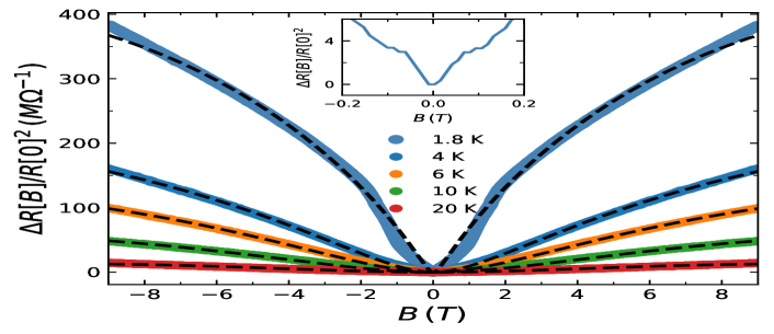
The formula for 3D WAL is provided by Fukuyama and Hoshino (F-H) Fukuyama and Hoshino (1981); Baxter et al. (1989). The correction due to electronic correlation consists of two parts. The orbital part is calculated by Altshuler et al. Al’tshuler et al. (1981) and the spin part is calculated by Lee and Ramakrishnan Lee and Ramakrishnan (1982). Alternative expressions for the orbital part are also available Altshuler and Aronov (1985); Isawa and Fukuyama (1984). These formula are suspected to fail at high fields Richter et al. (1988); Wu and Lin (1994) and many fits to experimental data show clear deviations Sahnoune et al. (1992); Biggs et al. (1990); Li and Lin (1997). Therefore, we generate the dashed fitted lines in Fig. 4(a) merely to show that the magnetoresistance of HfNiSn is a typical WAL magnetoresistance, but the fitting parameters will not be discussed here.
WAL has become an important tool to extract the electron dephasing scattering times Sahnoune et al. (1992); Biggs et al. (1990); Li and Lin (1997); Wu and Lin (1994). The critic field contained in the F-H formula is inversely proportional to . , where stands for () inelastic, () spin-flipping or () spin-orbit scattering respectively, and D is the temperature independent diffusion coefficient related to elastic scattering Fukuyama and Hoshino (1981); Wu and Lin (1994); Bieri et al. (1984). Because of the aforementioned reason, instead of fitting the magnetoresistance, we adopt another approach to get the temperature dependence of .
At low field and low temperature, . Utilizing the low field analytic expression of the function provided by Ousset et al. Ousset et al. (1985), the F-H formula reduces to a very simple form.
| (1) |
where , and is a constant related to the geometry of the sample.
provides information on different scattering mechanisms. , where is a temperature independent scattering time due to magnetic impurities. Usually, , where is the electron-electron scattering time and is the electron-phonon scattering time. It has been established that , where can be 2, 3 or 4 Li and Lin (1997); Komnik et al. (1994). In disordered systems, at low temperature, , where is the dimension of the electronic transport in the material Altshuler and Aronov (1985); Li and Lin (1997); Schmid (1974).
At low fields, utilizing the analytic expression of the function provided by Ousset et al. Ousset et al. (1985), the orbital part of the correction due to electronic correlation becomes
| (2) |
where , , is the temperature independent electron-phonon coupling constant Grimvall (1976); Allen (1999), is Euler’s constant and is a cut off temperature.
Utilizing the analytic expression of the function provided by Ousset et al. Ousset et al. (1985), the spin part becomes
| (3) |
Where , is the electron spin g-factor, is the Bohr magneton, is the screening parameter for the Coulomb interaction.
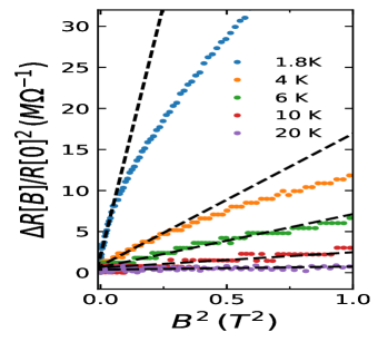
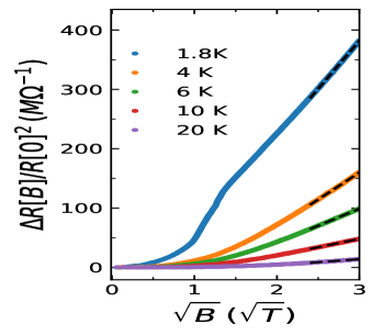
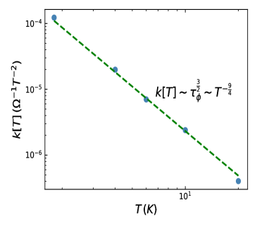
The data clearly follows a dependence at low fields. Taken together, Eqs. 1, 2 and 3 indicate that where the slopes of the dashed lines in Fig. 4(b) indicates the values of . The determined values of are very robust. For example, in the analysis of the magnetoresistance, regressions are performed using increasing numbers of data points from to . The calculated slowly decreases from to which will not qualitatively change the conclusion. Figure 5 is the log-log plot of versus . The almost linear relation represents either the term in Eq. 2 and 3 or one of the scattering mechanisms in dominates. By minimizing the mean squared error of , the green dashed line in Fig. 5 is generated using only Eq. 1 and supposing that , when only the 3D electron-electron scattering is considered. One could also attempt to fit to an expression that includes Eq. 1, 2, 3 and all possible terms in . However, when the term in Eq. 2 is excluded, no better fitting can be generated than simply including the effect of electron-electron scatterings. Therefore, the magnetoresistance supports a strong electronic correlation and a 3D electronic transport in HfNiSn.
III.3 Conductivity
According to McMillan McMillan (1981), Altshuler and Aronov Altshuler and Aronov (1985), electronic correlation leads to a quantum correction to the the Boltzmann conductivity in weakly disordered systems, . This relation correctly describes the typical low temperature conductivity of HfNiSn from to around .
High temperature conductivity of HfNiSn implies a gap of to Aliev et al. (1989); Ahilan et al. (2004); Cook et al. (1999). Our flux-grown HfNiSn single crystals also show an activated conductivity above . But the calculated gap is around . In the tunneling conductance, there is a small upturn at shown in the inset of Fig. 3(b). If the upturn indicates the band edge, the tunneling conductance also indicates a comparable gap of and the ZBA probably lies in an impurity band.
IV Conclusion
In conclusion, we observed ZBA of various power laws in the STS of ZrNiPb, HfNiSn and NbFeSb. These ZBA, that are probably in the impurity band, are the result of disorder and strong electronic correlations. Within the framework of traditional ab initio methods, it is difficult to explain these ZBA and consequent properties of half-Heusler compounds with 18 valence electrons. Similarly, the discussions of doping experiments of these compounds should be reexamined. From the magnetoresistance of HfNiSn, we found that below , the inelastic scattering time is proportional to , which indicates that electron-electron scattering dominates. We also showed that the low temperature conductivity of HfNiSn obeys , also indicating a strong electronic correlation.
References
- Yu et al. (2010) C. Yu, T.-J. Zhu, K. Xiao, J.-J. Shen, S. h. Yang, and X. b. Zhao, J. Electron. Mater. 39, 2008 (2010).
- Xie et al. (2012) H.-H. Xie, J.-L. Mi, L.-P. Hu, N. Lock, M. Chirstensen, C.-G. Fu, X.-B. Z. B. B. Iversen, and T.-J. Zhu, Cryst. Eng. Comm. 14, 4467 (2012).
- Wang et al. (2010) S.-H. Wang, H.-M. Cheng, R.-J. Wu, and W.-H. Chao, Thin Solid Films 518, 5901 (2010).
- Chen and Ren (2013) S. Chen and Z. Ren, Mater. Today 16, 387 (2013).
- Hohl et al. (1999) H. Hohl, A. P. Ramirez, C. Goldmann, and G. Ernst, J. Phys.: Condens. Matter 11, 1697 (1999).
- Uher et al. (1999) C. Uher, J. Yang, S. Hu, D. T. Morelli, and G. P. Meisner, Phys. Rev. B 59, 8615 (1999).
- Bhardwaj et al. (2012) A. Bhardwaj, D. K. Misra, J. J. Pulikkotil, S. Auluck, A. Dhar, and R. C. Budhani, Appl. Phys. Lett. 101, 133103 (2012).
- Makongo et al. (2011) J. P. A. Makongo, D. K. Misra, X. Zhou, et al., J. Am. Chem. Soc. 133, 18843 (2011).
- Aliev et al. (1989) F. G. Aliev, N. B. Brandt, V. V. Moshchalkov, et al., Z. Phys. B 75, 167 (1989).
- Berche and Jund (2018) A. Berche and P. Jund, Materials 11 (2018).
- Tang et al. (2018) Y. L. Tang, X. S. Li, L. H. J. Martin, E. C. Reyes, T. Ivas, C. Leinenbach, S. Anand, M. Peters, G. J. Snyder, and C. Battaglia, Energy Environ. Sci. 11, 311 (2018).
- Tian et al. (2018) Y. Tian, H. Zhu, W. Ren, et al., Phys. Chem. Chem. Phys. 20, 21960 (2018).
- McMillan and Mochel (1980) W. L. McMillan and J. Mochel, Phys. Rev. Lett 46, 556 (1980).
- Raychaudhuri et al. (1995) A. K. Raychaudhuri, K. P. Rajeev, H. Srikanth, and N. Gayathri, Phys. Rev. B 51, 7421 (1995).
- Colinet et al. (2014) C. Colinet, P. Jund, and J.-C. Tédenac, Intermetallics 46, 103 (2014).
- Hertel et al. (1983) G. Hertel, D. J. Bishop, E. G. Spencer, et al., Phys. Rev. Lett. 50, 743 (1983).
- Lee et al. (1999) M. Lee, J. G. Massey, V. L. Nguyen, and B. I. Shklovskii, Phys. Rev. B 60, 1582 (1999).
- Steinke et al. (2018) L. Steinke, J. J. Kistner-Morris, T. F. Lovorn, H. He, A. D. Hillier, P. Miao, S. Zellman, M. Klemm, M. Green, O. Gonzalez, A. H. MacDonald, and M. C. Aronson, ArXiv e-prints (2018), arXiv:1805.06337 [cond-mat.mtrl-sci] .
- Libioulle et al. (1995) L. Libioulle, Y. Houbion, and J.-M. Gilles, Rev. Sci. Instrum. 66, 97 (1995).
- Altshuler and Aronov (1985) B. L. Altshuler and A. G. Aronov, “Electron-electron interactions in disordered systems,” (North-Holland Physics Publishing, 1985) Chap. Electron-Electron Interaction in Disordered Conductors.
- Imry and Ovadyahu (1982a) Y. Imry and Z. Ovadyahu, Phys. Rev. Lett. 49, 841 (1982a).
- Imry and Ovadyahu (1982b) Y. Imry and Z. Ovadyahu, J. Phys. C: Solid State Phys. 15, L327 (1982b).
- Mao et al. (2017) J. Mao, J. Zhou, H. Zhu, et al., Chem. Mater. 29, 867 (2017).
- Fang et al. (2016) T. Fang, S. Zheng, H. Chen, et al., RSC Adv. 6, 10507 (2016).
- Massey and Lee (1995) J. G. Massey and M. Lee, Phys. Rev. Lett. 75, 4266 (1995).
- Levin et al. (1987) E. I. Levin, V. L. Nguen, B. I. Shklovsiǐ, and A. L. Éfros, Zh. Eksp. Teor. Fiz. 92, 1499 (1987).
- Sarma et al. (1998) D. D. Sarma, A. Chainani, and S. R. Krishnakumar, Phys. Rev. Lett. 80, 4004 (1998).
- Kirtley and Scalapino (1990) J. R. Kirtley and D. J. Scalapino, Phys. Rev. Lett. 65, 798 (1990).
- Kopietz (1998) P. Kopietz, Phys. Rev. Lett. 81, 2120 (1998).
- Butko et al. (2000) V. Y. Butko, J. F. DiTusa, and P. W. Adams, Phys. Rev. Lett. 84, 1543 (2000).
- Efros and Shklovskii (1985) A. L. Efros and B. I. Shklovskii, “Electron-electron interactions in disordered systems,” (Elsevier, 1985) Chap. Coulomb interaction in disordered systems with localized electronic states.
- Olivier et al. (1986) M. Olivier, J. O. Strom-Olsen, and Z. Altounian, Phys. Rev. B 33 (1986).
- Trudeau and Cochrane (1988) M. L. Trudeau and R. W. Cochrane, Phys. Rev. B 38 (1988).
- Rosenbaum et al. (1981) T. F. Rosenbaum, R. F. Milligan, G. A. Thomas, P. A. Lee, T. V. Ramakrishnan, and R. N. Bhatt, Phys. Rev. Lett. 47, 1758 (1981).
- Biggs et al. (1990) B. D. Biggs, S. J. Poon, and N. R. Munirathnam, Phys. Rev. Lett. 65, 2700 (1990).
- Nakajima et al. (2016) Y. Nakajima, P. Syers, X. F. Wang, R. X. Wang, and J. Paglione, Nat. Phys. 12, 213 (2016).
- Bao et al. (2012) L. H. Bao, L. He, N. Meyer, X. F. Kou, P. Zhang, Z. G. Chen, A. V. Fedorov, J. Zou, T. M. Riedemann, T. A. Lograsso, K. L. Wang, G. Tuttle, and F. X. Xiu, Sci. Rep. 2 (2012).
- Fukuyama and Hoshino (1981) H. Fukuyama and K. Hoshino, J. Phys. Soc. Jpn. 50, 2131 (1981).
- Baxter et al. (1989) D. V. Baxter, R. Richter, M. L. Trudeau, R. W. Cochrane, and J. O. Strom-Olsen, Journal de Physique 50, 1673 (1989).
- Al’tshuler et al. (1981) B. L. Al’tshuler, A. G. Aronov, A. I. Larkin, and D. E. Khmel’nitksiǐ, Sov. Phys. JETP 54, 411 (1981).
- Lee and Ramakrishnan (1982) P. A. Lee and T. V. Ramakrishnan, Phys. Rev. B 26, 4009 (1982).
- Isawa and Fukuyama (1984) Y. Isawa and H. Fukuyama, J. Phys. Soc. Jpn. 53, 1415 (1984).
- Richter et al. (1988) R. Richter, D. V. Baxter, and J. O. Strom-Olsen, Phys. Rev. B 38, 10421 (1988).
- Wu and Lin (1994) C. Y. Wu and J. J. Lin, Phys. Rev. B 50, 385 (1994).
- Sahnoune et al. (1992) A. Sahnoune, J. O. Ström-Olsen, and A. Zaluska, Phys. Rev. B 46 (1992).
- Li and Lin (1997) T.-J. Li and J. J. Lin, Phys. Rev. B 56 (1997).
- Bieri et al. (1984) J. B. Bieri, A. Fert, and G. Creuzet, J. Appl. Phys. 55, 1948 (1984).
- Ousset et al. (1985) J. C. Ousset, S. Askenazy, H. Rakoto, and J. M. Broto, Journal de Physique 46, 2145 (1985).
- Komnik et al. (1994) Y. F. Komnik, V. Y. Kashirin, B. I. Belevtsev, and E. Y. Beliaev, Phys. Rev. B 50, 15298 (1994).
- Schmid (1974) A. Schmid, Z. Physik 271, 251 (1974).
- Grimvall (1976) G. Grimvall, Phys. Scr. 14, 63 (1976).
- Allen (1999) P. B. Allen, “Handbook of superconductivity,” (Academic Press, 1999) p. 478.
- Ahilan et al. (2004) K. Ahilan, M. C. Bennett, M. C. Aronson, N. E. Anderson, P. C. Canfield, E. Munoz-Sandoval, T. Gortenmulder, R. Hendrikx, and J. A. Mydosh, Phys. Rev. B 69, 245116 (2004).
- Cook et al. (1999) B. A. Cook, G. P. Meisner, J. Yang, and C. Uher, in Eighteenth International Conference on Thermoelectrics. Proceedings, ICT’99 (Cat. No.99TH8407) (1999) p. 64.
- McMillan (1981) W. L. McMillan, Phys. Rev. B 24, 2739 (1981).
- Kaveh and Mott (1982) M. Kaveh and N. F. Mott, J. Phys. C: Solid State Phys. 15, L707 (1982).
- Howson and Greig (1984) M. A. Howson and D. Greig, Phys. Rev. B 30, 4805 (1984).
- Dodson et al. (1981) B. W. Dodson, W. L. McMillan, and J. M. Mochel, Phys. Rev. Lett. 46, 46 (1981).
- Schmid (1973) A. Schmid, Z. Physik 259, 421 (1973).
- Quan et al. (2014) Z.-Y. Quan, L. Zhang, W. Liu, et al., Nanoscale Res. Lett. 9, 6 (2014).
- Xu et al. (1995) Y. Xu, D. Ephron, and M. R. Beasley, Phys. Rev. B 52, 2843 (1995).
- Glazman and Matveev (1988) L. I. Glazman and K. A. Matveev, Zh. Eksp. Teor. Fiz. 94, 332 (1988).