Effect of O-doping or N-vacancy on the structural, electronic and magnetic properties of MoSi2N4 monolayer
Abstract
In this letter, the effect of four types of defects (ONout, ONin, VNout and VNin) on the structural, electronic and magnetic properties of MoSi2N4 monolayer were investigated using first-principles calculations. The calculated results reveal that all the four types of defects lead to structural distortions around the O-dopant or N-vacancy, and thereby change the lattice parameter and monolayer height . Specifically, ONout or ONin increases the lattice parameter, but VNout or VNin is on the contrary. ONout or VNout increases the monolayer height, whereas the height decreases for ONin or VNin. Each of the four types of defects has a fundamental effect on the electronic properties of MoSi2N4 monolayer, which can induce a transition from semiconductor to metal. ONin or VNin plays a vital role in the occurrence of a transition from non-magnetism to ferrimagnetism in MoSi2N4 monolayer. The effect of biaxial strain on the magnetic properties of the two systems with ONin and VNin was subsequently investigated. It is found that the total magnetic moments are less sensitive to biaxial strain whereas the local magnetic moments residing on the Mo atoms are increased for the two systems with ONin and VNin, as strain increases from -3% to 10% and from -9% to 10%, respectively. Furthermore, the magnetic phase transitions between ferrimagnetic and paramagnetic states were found to occur around -4% strain and within the range of -10% -9% for the two systems with ONin and VNin, respectively. This study may provide a guidance for the application of MoSi2N4 monolayer in the spintronic and magnetic materials.
Two-dimensional (2D) materials, exhibiting physical and chemical properties that are richer than and completely different from the 3D bulk crystals due to the inherent quantum confinement effect along the direction of atomic-layered height, and thus have drawn considerable attentions from the scientific and industrial circles on a global scale in the past few years. The most typical and also earliest 2D material confirmed experimentally is graphene [1], which possesses unique electrical properties. Researchers subsequently got inspirations from it and developed a series of new 2D materials with excellent mechanical, thermodynamic, electrical, optical and magnetic properties, opening up another valuable path for the development and investigation of high-performance electronic devices, optoelectronic devices, spintronic devices, as well as energy conversion and storage fields [2, 3, 4, 5].
The MoSi2N4 compound, a novel synthetic 2D layered van der Waals (vdW) material without known 3D layered parents fabricated very recently by Hong et al. [6] through chemical vapor deposition (CVD) technology, are attracting great interest in the optoelectronics, valleytronics, spintronics and so on. The synthesis of such material provides a huge opportunity for engineering materials with new attributes and functionality [7]. Hong et al. studied the MoSi2N4 monolayer film and reported that it is built up by septuple-atomic-layer of N-Si-N-Mo-N-Si-N, and exhibits non-magnetic semiconducting nature, high strength, as well as excellent ambient stability. They investigated its optical properties and evaluated the band gap via Tauc plot analysis further, and employed density functional theory (DFT) [8, 9] to explain observed phenomena. It is found that the MoSi2N4 monolayer possesses an indirect band gap of 1.94 eV and displays a high optical transmittance with an average of 97.5 0.2% in the visible range, and the spin-orbit coupling (SOC) existing in the valence band (VB) can be used to elucidate the two sub-peaks in the optical absorption spectrum. Wang et al. [10] analyzed the crystal structure possessing septuple-atomic-layered characteristic for the MoSi2N4 monolayer and reported that it can be viewed as the insertion of the triple-atomic-layered 2-MoS2-type MoN2 monolayer into the quadruple-atomic-layered -InSe-type Si2N2 monolayer. The piezoelectric and electronic properties of MoSi2N4 monolayer under strain within the range from -4% to 4% were studied by Guo et al. [11] and found that the biaxial tensile strain can enhance the piezoelectric strain coefficient 11 and spin-orbit splitting at K point, whereas the band gap decreases with increasing strain. Guo et al. [12] investigated the effect of large biaxial strain ranging from -10% to 10% on the electronic structure, transport and piezoelectric coefficients of MoSi2N4 monolayer and reported that as strain increases from -10% to 10%, the band gap first increases and then decreases. Bafekry et al. [13] explored the structural, mechanical, thermal, electronic, optical and photocatalytic properties of MoSi2N4 monolayer and found that it possesses a good thermoelectric performance, and its work function is very similar to that of phosphorene and MoS2 monolayers. Kang et al. [14] studied the second harmonic generation (SHG) effects of typical MoSi2N4 phases and reported that the two most typical phases may exhibit different SHG intensities due to the difference in P between the outer and inner layers of the sandwich structure. Li et al. [15] and Yang et al. [16] explored the valley-dependent properties of MoSi2N4 monolayer and found that it is a semiconductor with a pair of Dirac-type valleys located at the corners of the hexagonal Brillouin zone and can realize the valley-contrast properties, suggesting that its potential applications in valleytronic and spintronic devices. Moreover, Cao et al. [17] investigated the vdW heterostructures composed of MoSi2N4 vertically contacted by graphene and NbS2 monolayers and showed that MoSi2N4/NbS2 contact exhibits an ultralow Schottky barrier height (SBH), and the SBH can be modulated via interlayer distance or external electric fields for MoSi2N4/graphene contact, opening up an opportunity for reconfigurable and tunable nanoelectronic devices.
As is well known, the physical and chemical properties of 2D materials under diverse conditions and requirements can commonly be effectively modulated by using of defect, strain, external electric field [18, 19, 20, 21, 22, 23, 24, 25, 26, 27] and so on, which provides convenience for investigating the optical, electrical, magnetic and topological properties etcetera closely related to the electronic structure. Despite an increasing theoretical exploration toward MoSi2N4 monolayer recently, to date the effect of defect on its physical properties has not yet been investigated. Besides, such work is significant to understand the natures of MoSi2N4 compound and develop its practical applications further.
In view of the facts, herein we targeted to view the structural, electronic and magnetic properties of MoSi2N4 monolayer induced by the defects with O-doping and N-vacancy using first-principles approach based on DFT. The electronic and magnetic properties were studied through GGA + SOC and GGA + Spin Polarization calculations, respectively. The calculated results of intrinsic MoSi2N4 monolayer were also given in this letter for comparison.
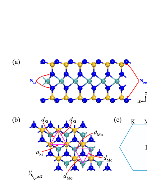
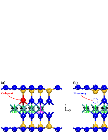
Considering that there are two types of N atomic layers according to the symmetry of septuple-atomic-layered MoSi2N4 monolayer, namely the outer and inner layers, which were respectively marked with Nout and Nin in Fig. 1(a) for the convenience of description. For the substitutional doping type of defects, the O atom is treated as dopant to substitute for one N atom in the Nout and Nin respectively, which were respectively denoted as ONout and ONin. The vacancy type of defects come from the removal of one N atom in the Nout and Nin respectively, which were respectively labeled as VNout and VNin. Therefore there are four types of defects. The concentrations of these defects were all set to 6.25%, corresponding to the 2 2 1 super-cell. Throughout our calculations, the plane-wave pseudopotential method [28] within the framework of DFT implemented in the CASTEP code [29] was adopted. Norm-conserving pseudopotentials were applied to describe the interactions between ion-cores and valence electrons, and the generalized gradient approximation (GGA) functional following the Perdew-Burke-Ernzerhof (PBE) [30] scheme was employed to paint the electronic exchange-correlation potential. In order to minimize the interaction between the periodic layers along the c-axis direction, the vacuum slab of more than 24 Å between layers was adopted. All geometric structures were fully relaxed until the maximum force on each atom is less than 0.01 eV/Å. The cut-off energy for plan-wave expansion was set to 1100 eV and the Monkhorst-Pack [31] k-point grid of 11 11 1 in the Brillouin zone was applied to both the structural relaxation and self-consistent field (SCF) process with a convergence threshold of 1.0 10-7 eV/atom.
Figs. 1(a) and 1(b) present the side and top views of intrinsic MoSi2N4 monolayer respectively, which belongs to the hexagonal lattice with the P-6M2 space group (No. 187). The lattice parameter ( = ) of the unit cell, monolayer height and cohesive energy coh for intrinsic MoSi2N4 monolayer were calculated first to examine the validity of the DFT-PBE method employed in this letter. The calculated , and coh are respectively 2.932 Å, 7.075 Å and -8.573 eV/atom, which agree well with previous values [6, 11, 13, 15, 17, 32], indicating the accuracy of this method. Tab. 1 summarizes the Si-Si distances (labeled as Si in Fig. 1(b)) nearest to the O-dopant or N-vacancy in the Nout, Mo-Mo distances (labeled as Mo in Fig. 1(b)) nearest to the O-dopant or N-vacancy in the Nin, lattice parameter ( = ) of the 2 2 1 super-cell and monolayer height for intrinsic and four defective systems. It is clear from this table that the Si in the system with ONout and Mo in the system with ONin increase, whereas the Si in the system with VNout and Mo in the system with VNin decrease, compared with those of intrinsic system. Moreover, a little bigger for the system with ONout or ONin toward the lattice parameter than intrinsic system, yet the reduction of was found in the system with VNout or VNin. In addition, all the four types of defects can also have an effect on the height of MoSi2N4 monolayer. From Tab. 1, the height of the system with ONout or VNout is greater than that of intrinsic system. Nevertheless, the becomes smaller for the system with ONin or VNin. It is shown that the increase or decrease of may be independent of the implementation of O-doping or N-vacancy, which is only related to which N atomic layer the O-doping or N-vacancy actualized in. Furthermore, the monolayer height will increase for O-doping or N-vacancy actualized in the Nout; on the contrary, it will decrease for that implemented in the Nin.
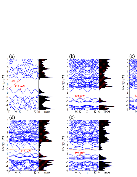
The calculated electronic band structures along the high symmetric paths in the 1st Brillouin zone (Fig. 1(c)) and corresponding total density of states (TDOS) incorporating SOC of intrinsic and four defective systems are displayed in Figs. 2(a) 2(e), respectively. For the intrinsic system, the valence band maximum (VBM) is located at the point whereas the conduction band minimum (CBM) is located at the K point, indicating an indirect band gap semiconductor characteristic (see Fig. 2(a)). The calculated band gap value is 1.953 eV, which is in good accordance with previous result (1.940 eV) evaluated by Hong et al. [6] through Tauc plot analysis. Furthermore, the calculated spin-orbit splitting in the VB at K point is 126 meV, which is highly consistent with previous data available [6, 11, 12, 15]. Interestingly enough, a transition from semiconductor to metal induced by each of the four types of defects was observed in MoSi2N4 monolayer. In other words, for the system with ONout, ONin, VNout or VNin, it is quite evident that each of them exhibits metallic characteristic with two dispersive energy band passing over the Fermi level (see Figs. 2(b) 2(e)). Moreover, the spin-orbit splitting values are respectively 130, 120, 126 and 100 meV for the four systems with ONout, ONin, VNout and VNin. Compared with the splitting value of intrinsic system, there is a tiny increasement for that of the system with ONout. But for the system with ONin or VNin, the splitting value decreases. It is suggested that all the ONout, ONin and VNin have a marginal effect on the spin-orbit coupling in MoSi2N4 monolayer.
We detected the Mulliken overlap populations [33] between the center N atom in the Nout and its three Si ligands, the center N atom in the Nin and its three Mo ligands for the intrinsic system further. It is found that the average overlap populations of the three N-Si and three N-Mo bonds are 1.45 and 0.94, respectively. The absolute values of the overlap populations reflect the level of covalent properties for the N-Si and N-Mo bonds, and also mean the extent of the electron sharing between them. However, the average overlap populations of the three O-Si bonds in the system with ONout and three O-Mo bonds in the system with ONin are -0.25 and -0.02, respectively. It is shown that both the O-Si and O-Mo bonds exhibit antibonding states, implying there exist repulsive interactions, which may be the causes for the larger Si in the system with ONout, Mo in the system with ONin and in the two systems with ONout and ONin. Conversely, the removal of one N atom in the Nout or Nin from the intrinsic MoSi2N4 monolayer causes structural constrictions of the three Si atoms or three Mo atoms surrounding the N-vacancy. Three bonding electrons in the system with VNout or four bonding electrons in the system with VNin are removed while the formation of N-vacancy. Such a close neighbor of the vacancy of the Si atoms or Mo atoms will appear three effective charges of dangling bonds. For the intrinsic system, the average charges of the three Si atoms directly bonding with the center N atom in the Nout and three Mo atoms directly bonding with that in the Nin are respectively 1.03e and 0.06e, according to the calculated Mulliken atomic populations. Nonetheless, the average charge of 0.64e was observed on the three Si atoms nearest to the N-vacancy in the system with VNout, and the average charge of the three Mo atoms nearest to the N-vacancy in the system with VNin is -0.06e. It is shown that the electron density residing on the three Si atoms or three Mo atoms is increased. Such charge redistribution can be seen as the micro-explanation for the reductions of Si in the system with VNout, Mo in the system with VNin and in the two systems with VNout and VNin.
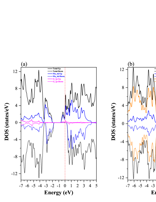
The spin polarized calculations without SOC and given initial magnetic configuration were performed to analyze the magnetic behavior. According to the calculated Mulliken atomic populations, the total magnetic moments tot of intrinsic and four defective systems are also tabulated in Tab. 1. From this table, the intrinsic MoSi2N4 monolayer possesses no magnetic moment, which is consistent with previous result calculated by Hong et al. [6], showing that this calculation method is reliable. For the four defective systems, the total magnetic moment of the system with ONout or VNout is also zero. Nevertheless, a tot of 1.000B was observed in the system with ONin or VNin. As displayed in Fig. 3(a), the partial density of states (PDOS) of Mo and O atoms implies that the total magnetic moment mainly originates from the strong coupling between the 4d states of Mo and 2p state of O for the system with ONin. For the system with VNin, the PDOS of Mo and N atoms suggests that the total magnetic moment primarily comes from the strong coupling between the 4d states of Mo and 2p state of N, as shown in Fig. 3(b).
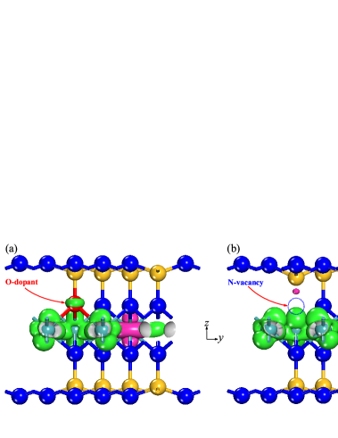
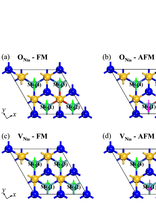
We inspected the local magnetic moments of the two systems with ONin and VNin further. Figs. 4(a) and 4(b) show the side views of net spin density for the two systems with ONin and VNin, respectively. As shown in these figures, the total magnetic moment is notably contributed from the local magnetic moments residing on the Mo atoms. According to these local magnetic moments, the magnetic structures for both of these systems can be demonstrated. Figs. 5(a) and 5(b) present the detailed magnetic moment arrangements within a super-cell in the two systems with ONin and VNin, respectively. From these figures, the local magnetic moments of Mo(1), Mo(2) and Mo(3) atoms around the O-dopant or N-vacancy are equivalent to each other, exhibiting up-spin states, and the magnitudes are 0.520B and 0.580B per Mo atom for the two systems with ONin and VNin, respectively. However, the remaining one Mo(4) atom possesses a local magnetic moment with down-spin state, and the magnitudes are -0.470B and -0.410B per Mo atom for the two systems with ONin and VNin, respectively. It can be concluded that such magnetic moment arrangement displays a magnetic structure with ferrimagnetic (FRM) ordering for the system with ONin or VNin.
In order to verify the magnetic structure further, two different initial magnetic configurations within the 2 2 1 super-cells of the system with ONin or VNin were given, namely, one ferromagnetic (FM) and one antiferromagnetic (AFM) initial states (see Figs. 6(a) 6(d)). We found that whatever the initial magnetic configuration is, the system with ONin or VNin becomes a ferrimagnetic state finally which is the same as that (see Figs. 5(a) and 5(b)) obtained using spin polarized calculations without given initial magnetic configuration. It is indicated that the system with ONin or VNin should possess a ferrimagnetic ground state.
Next, the effect of biaxial strain on the magnetic properties of the two systems with ONin and VNin was discussed. Here, the biaxial strain is defined as
| (1) |
where and 0 are the strained and unstrained lattice parameters, respectively. The positive (negative) represents the tensile (compressive) strain, and a strain range from -10% to 10% was applied to both of these systems. Tab. 2 and Tab. 3 list the calculated total magnetic moment tot, local magnetic moments residing on the Mo atoms Mo(1), Mo(2), Mo(3) and Mo(4) of the two systems with ONin and VNin under different strains, respectively. From Tab. 2, it is obvious that the system with ONin exhibits a ferrimagnetic state within the range of -3% 10%. The variation of tot is negligible as strain increases from -3% to 10%, indicating that the tot is less sensitive to biaxial strain. Nevertheless, the Mo(1), Mo(2), Mo(3) and Mo(4) are all increased. It is worth noting that the local magnetic moments residing on the Mo(1), Mo(2) and Mo(3) atoms are still equivalent to each other, which may be associated with the unbroken lattice symmetry under biaxial strain. Moreover, the tot, Mo(1), Mo(2), Mo(3) and Mo(4) are all zero within the range of -10% -5%, indicating this system shows a paramagnetic state. We found that the tot, Mo(1), Mo(2), Mo(3) and Mo(4) at -4% strain are all difficult to calculate, cannot be obtained, and thus the data at such strain are not given in Tab. 2. Therefore we suggest that there exists a magnetic phase transition between ferrimagnetic and paramagnetic states around -4% strain. For the system with VNin, it is clear from Tab. 3 that it presents a ferrimagnetic state within the range of -9% 10%. Analogously, the tot is also less sensitive to biaxial strain, the Mo(1), Mo(2), Mo(3) and Mo(4) are all increased, the local magnetic moments of Mo(1), Mo(2) and Mo(3) atoms are still equivalent to each other, as strain increases from -9% to 10%. However, the tot, Mo(1), Mo(2), Mo(3) and Mo(4) are all zero at -10% strain, suggesting this system displays a paramagnetic state. We calculated these magnetic moments at -11% strain further and found that all of them are also zero. It is shown that there also exists a magnetic phase transition between ferrimagnetic and paramagnetic states within the range of -10% -9%.
In conclusion, we systematically investigated the structural, electronic and magnetic properties of MoSi2N4 monolayer induced by the four types of defect (ONout, ONin, VNout and VNin), using first-principles density functional theory calculations. Our results reveal that all the four types of defects lead to structural distortions around the O-dopant or N-vacancy, and thereby change the lattice parameter and monolayer height . Specifically, ONout or ONin increases the lattice parameter, but VNout or VNin is on the contrary. ONout or VNout increases the monolayer height, whereas the height decreases for ONin or VNin. Each of the four types of defects has a fundamental effect on the electronic properties of MoSi2N4 monolayer, which can induce a transition from semiconductor to metal. ONin or VNin plays a vital role in the occurrence of a transition from non-magnetism to ferrimagnetism in MoSi2N4 monolayer. Subsequently, the effect of biaxial strain on the magnetic properties of the two systems with ONin and VNin was investigated. It is found that the total magnetic moments are less sensitive to biaxial strain, the local magnetic moments residing on the Mo atoms are increased for the two systems with ONin and VNin, as strain increases from -3% to 10% and from -9% to 10%, respectively. Furthermore, the magnetic phase transitions between ferrimagnetic and paramagnetic states were found to occur around -4% strain and within the range of -10% -9% for the two systems with ONin and VNin, respectively. This study may provide a guidance for the application of MoSi2N4 monolayer in the spintronic and magnetic materials.
References
- [1] K. S. Novoselov, A. K. Geim, S. V. Morozov, D. Jiang, Y. Zhang, S. V. Dubonos, I. V. Grigorieva, and A. A. Firsov. Electric field effect in atomically thin carbon films. Science, 306(5696):666–669, 2004.
- [2] Chanyoung Yim, Kangho Lee, Niall McEvoy, Maria O’Brien, Sarah Riazimehr, Nina C. Berner, Conor P. Cullen, Jani Kotakoski, Jannik C. Meyer, Max C. Lemme, and Georg S. Duesberg. High-performance hybrid electronic devices from layered ptse2 films grown at low temperature. ACS Nano, 10(10):9550–9558, 2016. PMID: 27661979.
- [3] Britton W. H. Baugher, Hugh O. H. Churchill, Yafang Yang, and Pablo Jarillo-Herrero. Optoelectronic devices based on electrically tunable p–n diodes in a monolayer dichalcogenide. Nature Nanotechnology, 9(4):262–267, Apr 2014.
- [4] Kin Fai Mak, Keliang He, Jie Shan, and Tony F. Heinz. Control of valley polarization in monolayer mos2 by optical helicity. Nature Nanotechnology, 7(8):494–498, Aug 2012.
- [5] Marco Bernardi, Maurizia Palummo, and Jeffrey C. Grossman. Extraordinary sunlight absorption and one nanometer thick photovoltaics using two-dimensional monolayer materials. Nano Letters, 13(8):3664–3670, 2013. PMID: 23750910.
- [6] Yi-Lun Hong, Zhibo Liu, Lei Wang, Tianya Zhou, Wei Ma, Chuan Xu, Shun Feng, Long Chen, Mao-Lin Chen, Dong-Ming Sun, Xing-Qiu Chen, Hui-Ming Cheng, and Wencai Ren. Chemical vapor deposition of layered two-dimensional mosi2n4 materials. Science, 369(6504):670–674, 2020.
- [7] Kostya S Novoselov. Discovery of 2D van der Waals layered MoSi2N4 family. National Science Review, 08 2020. nwaa190.
- [8] P. Hohenberg and W. Kohn. Inhomogeneous electron gas. Phys. Rev., 136:B864–B871, Nov 1964.
- [9] W. Kohn and L. J. Sham. Self-consistent equations including exchange and correlation effects. Phys. Rev., 140:A1133–A1138, Nov 1965.
- [10] Lei Wang, Yongpeng Shi, Mingfeng Liu, Yi-Lun Hong, Ming-Xing Chen, Ronghan Li, Qiang Gao, Wencai Ren, Hui-Ming Cheng, Yiyi Li, and Xing-Qiu Chen. Structure-driven intercalated architecture of septuple-atomic-layer family with diverse properties from semiconductor to topological insulator to ising superconductor, 2020.
- [11] San-Dong Guo, Yu-Tong Zhu, and Wen-Qi Mu. Intrinsic piezoelectricity in monolayer (x=ti, zr, hf, cr, mo and w), 2020.
- [12] Xiao-Shu Guo and San-Dong Guo. Tuning electronic structures, transport and piezoelectric coefficients of monolayer with biaxial strain, 2020.
- [13] A. Bafekry, M. Faraji, Do M. Hoat, M. M. Fadlallah, M. Shahrokhi, F. Shojaei, D. Gogova, and M. Ghergherehchi. Mosi2n4 single-layer: a novel two-dimensional material with outstanding mechanical, thermal, electronic, optical, and photocatalytic properties, 2020.
- [14] Lei Kang and Zheshuai Lin. Second harmonic generation of mosi2n4 layer, 2020.
- [15] Si Li, Weikang Wu, Xiaolong Feng, Shan Guan, Wanxiang Feng, Yugui Yao, and Shengyuan A. Yang. Valley-dependent properties of monolayer mosi2n4, wsi2n4 and mosi2as4, 2020.
- [16] Chen Yang, Zhigang Song, Xiaotian Sun, and Jing Lu. Valley pseudospin in monolayer mosi2n4 and mosi2as4, 2020.
- [17] Liemao Cao, Guanghui Zhou, L. K. Ang, and Yee Sin Ang. Two-dimensional van der waals electrical contact to monolayer mosi2n4, 2020.
- [18] Hongliang Shi, Hui Pan, Yong-Wei Zhang, and Boris I. Yakobson. Quasiparticle band structures and optical properties of strained monolayer mos2 and ws2. Phys. Rev. B, 87:155304, Apr 2013.
- [19] Anne Marie Z. Tan, Christoph Freysoldt, and Richard G. Hennig. First-principles investigation of charged dopants and dopant-vacancy defect complexes in monolayer . Phys. Rev. Materials, 4:114002, Nov 2020.
- [20] Asadollah Bafekry, Chuong Van Nguyen, Catherine Stampfl, Berna Akgenc, and Mitra Ghergherehchi. Oxygen vacancies in the single layer of ti2co2 mxene: Effects of gating voltage, mechanical strain, and atomic impurities. physica status solidi (b), n/a(n/a):2000343, 2020.
- [21] Aarti Shukla and N.K. Gaur. A dft study of defects in sno monolayer and their interaction with o2 molecule. Chemical Physics Letters, 754:137717, 2020.
- [22] Zhen Lin, Bin Fu, and Yukai An. Effects of defects and anions on the geometry, electronic structures and exchange interaction of fe-doped 2h-mose2 monolayer. Applied Surface Science, 528:146960, 2020.
- [23] Chen Wang and Yukai An. Effects of strain and stacking patterns on the electronic structure, valley polarization and magnetocrystalline anisotropy of layered vte2. Applied Surface Science, 538:148098, 2021.
- [24] Liangzhi Kou, Chun Tang, Yi Zhang, Thomas Heine, Changfeng Chen, and Thomas Frauenheim. Tuning magnetism and electronic phase transitions by strain and electric field in zigzag mos2 nanoribbons. The Journal of Physical Chemistry Letters, 3(20):2934–2941, 2012. PMID: 26292229.
- [25] Ai-Ming Hu, Ling ling Wang, Wen-Zhi Xiao, and Bo Meng. Electronic structures and magnetic properties in cu-doped two-dimensional dichalcogenides. Physica E: Low-dimensional Systems and Nanostructures, 73:69 – 75, 2015.
- [26] Asadollah Bafekry, Saber Farjami Shayesteh, Mitra Ghergherehchi, and Francois M. Peeters. Tuning the bandgap and introducing magnetism into monolayer bc3 by strain/defect engineering and adatom/molecule adsorption. Journal of Applied Physics, 126(14):144304, 2019.
- [27] Asadollah Bafekry, Catherine Stampfl, Mitra Ghergherehchi, and Saber Farjami Shayesteh. A first-principles study of the effects of atom impurities, defects, strain, electric field and layer thickness on the electronic and magnetic properties of the c2n nanosheet. Carbon, 157:371 – 384, 2020.
- [28] M. C. Payne, M. P. Teter, D. C. Allan, T. A. Arias, and J. D. Joannopoulos. Iterative minimization techniques for ab initio total-energy calculations: molecular dynamics and conjugate gradients. Rev. Mod. Phys., 64:1045–1097, Oct 1992.
- [29] S. J. Clark, M. D. Segall, C. J. Pickard, P. J. Hasnip, M. J. Probert, K. Refson, and M.C. Payne. First principles methods using CASTEP. Z. Kristall., 220:567–570, 2005.
- [30] John P. Perdew, Kieron Burke, and Matthias Ernzerhof. Generalized gradient approximation made simple. Phys. Rev. Lett., 77:3865–3868, Oct 1996.
- [31] Hendrik J. Monkhorst and James D. Pack. Special points for brillouin-zone integrations. Phys. Rev. B, 13:5188–5192, Jun 1976.
- [32] Hongxia Zhong, Wenqi Xiong, Pengfei Lv, Jin Yu, and Shengjun Yuan. Strain-induced semiconductor to metal transition in ma2z4 bilayers, 2020.
- [33] M. D. Segall, R. Shah, C. J. Pickard, and M. C. Payne. Population analysis of plane-wave electronic structure calculations of bulk materials. Phys. Rev. B, 54:16317–16320, Dec 1996.
| Systems | Si | Mo | tot | ||
|---|---|---|---|---|---|
| (Å) | (Å) | (Å) | (Å) | (B/super-cell) | |
| Intrinsic | 2.932 | 2.932 | 5.864 | 7.075 | 0.000 |
| ONout | 3.060 | — | 5.887 | 7.092 | 0.000 |
| ONin | — | 2.989 | 5.884 | 7.067 | 1.000 |
| VNout | 2.856 | — | 5.856 | 7.103 | 0.000 |
| VNin | — | 2.917 | 5.850 | 7.065 | 1.000 |
| Strain | tot | Mo(1) | Mo(2) | Mo(3) | Mo(4) |
|---|---|---|---|---|---|
| (B/super-cell) | (B/atom) | (B/atom) | (B/atom) | (B/atom) | |
| -10% | 0.000 | 0.000 | 0.000 | 0.000 | 0.000 |
| -8% | 0.000 | 0.000 | 0.000 | 0.000 | 0.000 |
| -6% | 0.000 | 0.000 | 0.000 | 0.000 | 0.000 |
| -5% | 0.000 | 0.000 | 0.000 | 0.000 | 0.000 |
| -4% | — | — | — | — | — |
| -3% | 0.997 | 0.330 | 0.330 | 0.330 | -0.120 |
| -2% | 1.000 | 0.340 | 0.340 | 0.340 | -0.140 |
| 0 | 1.000 | 0.520 | 0.520 | 0.520 | -0.470 |
| 2% | 0.999 | 0.560 | 0.560 | 0.560 | -0.510 |
| 4% | 0.969 | 0.590 | 0.590 | 0.590 | -0.590 |
| 6% | 0.975 | 0.680 | 0.680 | 0.680 | -0.820 |
| 8% | 1.000 | 0.880 | 0.880 | 0.880 | -1.340 |
| 10% | 1.000 | 1.100 | 1.100 | 1.100 | -1.920 |
| Strain | tot | Mo(1) | Mo(2) | Mo(3) | Mo(4) |
|---|---|---|---|---|---|
| (B/super-cell) | (B/atom) | (B/atom) | (B/atom) | (B/atom) | |
| -10% | 0.000 | 0.000 | 0.000 | 0.000 | 0.000 |
| -9% | 0.946 | 0.380 | 0.380 | 0.380 | -0.170 |
| -8% | 0.996 | 0.420 | 0.420 | 0.420 | -0.190 |
| -6% | 1.000 | 0.460 | 0.460 | 0.460 | -0.230 |
| -4% | 1.000 | 0.500 | 0.500 | 0.500 | -0.280 |
| -2% | 1.000 | 0.540 | 0.540 | 0.540 | -0.340 |
| 0 | 1.000 | 0.580 | 0.580 | 0.580 | -0.410 |
| 2% | 1.000 | 0.630 | 0.630 | 0.630 | -0.520 |
| 4% | 1.000 | 0.710 | 0.710 | 0.710 | -0.690 |
| 6% | 1.001 | 0.820 | 0.820 | 0.820 | -0.970 |
| 8% | 1.001 | 1.000 | 1.000 | 1.000 | -1.430 |
| 10% | 1.055 | 1.220 | 1.220 | 1.220 | -1.930 |