Low-Latency Asynchronous Logic Design
for Inference at the Edge
Abstract
Modern internet of things (IoT) devices leverage machine learning inference using sensed data on-device rather than offloading them to the cloud. Commonly known as inference at-the-edge, this gives many benefits to the users, including personalization and security. However, such applications demand high energy efficiency and robustness. In this paper we propose a method for reduced area and power overhead of self-timed early-propagative asynchronous inference circuits, designed using the principles of learning automata. Due to natural resilience to timing as well as logic underpinning, the circuits are tolerant to variations in environment and supply voltage whilst enabling the lowest possible latency. Our method is exemplified through an inference datapath for a low power machine learning application. The circuit builds on the Tsetlin machine algorithm further enhancing its energy efficiency. Average latency of the proposed circuit is reduced by compared with the synchronous implementation whilst maintaining similar area. Robustness of the proposed circuit is proven through post-synthesis simulation with supply. Functional correctness is maintained and latency scales with gate delay as voltage is decreased.
I Introduction
There is an accelerating demand for connected devices in the [ ([)\AC@linebreakpenalty]IoT [Capra2019]. Such devices often comprise a sensing aspect, collecting environmental or personal data, for providing useful monitoring and decisions for transforming our everyday life. The sensors collect vast amounts of data which must be processed into a usable or more manageable form. Traditionally this was done by offloading the data into cloud compute servers, usually over a wireless medium. However this paradigm is quickly becoming unmaintainable as [\AC@linebreakpenalty]IoT devices expand well into the billions [shafik2018real]. Generated data sizes become overwhelming, wireless data transmissions violate power budgets, and we see a shift towards data processing at the edge [arm-trillium]. Designers of [\AC@linebreakpenalty]IoT products are turning to [\AC@linebreakpenalty]ML in order to extract meaningful features from the sensed data. Such products are often powered by batteries or energy harvesters which demand low power and energy efficiency, as well as robustness to supply variations [shafik2018real].
There are several [\AC@linebreakpenalty]ML algorithms which may be suited to such applications, with [\AC@linebreakpenalty]NN in widespread usage thanks to their often state-of-the-art accuracy and powerful hardware/software ecosystem. HDC has also emerged in recent years with applications in low power systems [Burrello2020]. Recently the [\AC@linebreakpenalty]TM algorithm has been proposed as a promising [\AC@linebreakpenalty]ML algorithm based on Tsetlin automata—specialized learning automata. The Tsetlin automata use reinforcement learning locally, together creating an ensemble learning effect on the global scale which is used to compose logic clauses. Existing hardware based on [\AC@linebreakpenalty]TM offers a new direction for [\AC@linebreakpenalty]ML whose inference engine is based on logic with little arithmetic [Wheeldon2020b]. The logic-based underpinnings of the [\AC@linebreakpenalty]TM algorithm provide opportunities for low power and energy efficient [\AC@linebreakpenalty]ML hardware design in the [\AC@linebreakpenalty]IoT.
In this work we apply an asynchronous circuit design methodology [Wheeldon2019] to the [\AC@linebreakpenalty]TM algorithm. By removing the pairing between clock and supply voltage as in the synchronous digital designs, it enables an aggressive voltage scaling [Diamant2015] for reduced energy per inference and also adds robustness to environmental variations. Although we use [\AC@linebreakpenalty]ML as the key application driver, it is possible these techniques can also be applied in other application areas. Our method is built on dual-rail circuits with early propagation [Brej2006]. Dual-rail is an asynchronous circuit design style in the family of [\AC@linebreakpenalty]QDI circuits. It is inherently robust to circuit delay variations which means it can operate across a wide range of supply voltages and temperatures. This usually comes at the cost of duplicated logic and [\AC@linebreakpenalty]CD overhead [Yakovlev2013]. In our design we carefully select circuit topology to minimize such duplications. Additionally we use timing optimizations to reduce overhead from [\AC@linebreakpenalty]CD.
Nomenclature
Positive- and negative-rail signals are denoted and respectively. denotes the signal in the bit vector . V\texorpdfstring to s denotes a transition on a dual-rail signal from a valid codeword to a spacer. Vice versa for s\texorpdfstring to v.
Major Contributions of this paper
-
1.
application of early-propagative, reduced-overhead self-timed dual-rail circuits to [\AC@linebreakpenalty]ML inference; and
-
2.
analysis of operand and delay probability distributions in the [\AC@linebreakpenalty]ML inference circuit.
Paper Organization
Section II introduces the concepts of the [\AC@linebreakpenalty]TM algorithm. Section III first briefly introduces the principles of dual-rail circuits before describing our reduced [\AC@linebreakpenalty]CD scheme. Section IV presents our dual-rail inference datapath design with in-depth analyses. We finally conclude our findings in Section V.
II Tsetlin Machine Overview
The main inference component of the [\AC@linebreakpenalty]TM is the conjunctive clause which uses propositional logic expressions to produce a vote. The composition of each clause (determined by inclusion of literals) is controlled by the action outputs of a team of Tsetlin automata. For inference, the Tsetlin automata themselves are not required. Following a number of reinforcement steps, the automata decide whether their associated literal should be excluded from (action 1) or included in (action 2) the clause. Figure 1 illustrates a [\AC@linebreakpenalty]TM classifier with automaton teams and conjunctive clauses as one block for brevity.
Each clause can produce a vote for its class. Half of the clauses can vote positively, while the other half of the clauses can vote negatively. The inclusion of inhibition in the voting system enables non-linearity in the inference process. The votes are summed in a majority vote to produce a collective result which gives an indication of confidence. This confidence is used to influence future decisions of the automata [Granmo2018].
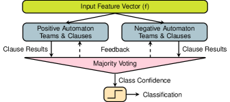
A simple thresholding function can be used to generate the final classification output. If the votes are positive (or zero), the input data is determined to belong to the class. For a negative sum the input data is determined to be not in the class.
For purposes of studying inference, we abstract the Tsetlin automaton action outputs to the circuit’s environment and concentrate on only the clauses calculation and majority voting.
III Self-timing Methodology
In dual-rail logic two wires are used to encode a codeword. For a single bit , the dual-rail encoding consists of the positive and negative rails . is encoded as , and is encoded as . One of the remaining states— or —is chosen to represent the empty state, referred to as a spacer, which separates valid codewords temporally so they can be distinguished from each other. Care must be taken to correctly handle spacer in the design, otherwise data hazards could occur where one valid overtakes another [Sokolov2006]. The remaining state is forbidden and must be avoided by design.
In our design we abide by the following requirements to ensure correct circuit operation:
Items 1, 6 and 5 are assumed as part of the circuit’s environment. To ensure Item 2, the circuit must be constructed solely from unate logic gates. To maintain monotonicity we must exclude non-unate logic gates (e.g. \textsmaller* gatexor and \textsmaller* gatexnor) from our library when generating the dual-rail netlist. Item 3 is taken care of by [\AC@linebreakpenalty]CD insertion. Item 4 can either be assumed as part of the environment or a delay can be added to the falling edge of [\AC@linebreakpenalty]CD assertion. The latter will be discussed in Section III-A.
III-A Reduced Completion Detection Scheme
[\AC@linebreakpenalty]CD which acknowledges both s\texorpdfstring to v and v\texorpdfstring to s at the [\AC@linebreakpenalty]PO is expensive to implement due to the vast amount of complex C-elements required [Sparso2001]. By indicating only s\texorpdfstring to v transitions we can significantly reduce the overhead of [\AC@linebreakpenalty]CD by using a small number of simple gates.
Full [\AC@linebreakpenalty]CD on internal signals is even more costly and removes the possiblity of early propagation. Its job is to ensure s\texorpdfstring to v and v\texorpdfstring to s occurs on internal nets for each operand. Internal [\AC@linebreakpenalty]CD can be safely omitted by giving a grace period for the internal signal to reset to spacer before applying new [\AC@linebreakpenalty]PI. Codeword validity and correct operation can still be guaranteed as long as Items 6, LABEL:, 5 and 4 are met.
In order to meet Item 4 there must be a sufficient grace period from application of spacer at the [\AC@linebreakpenalty]PI until application of the next valid at the [\AC@linebreakpenalty]PI. The grace period can be determined by using static timing analysis to find the maximum possible s\texorpdfstring to v time on all nodes of the circuit. Consequently the grace period can be guaranteed by either 1. the circuit environment waiting for the required grace period; or 2. an appropriate delay built into the done signal of the [\AC@linebreakpenalty]CD. The required delay can be calculated as , where is the maximum internal net v\texorpdfstring to s time, and is the maximum v\texorpdfstring to s time from the [\AC@linebreakpenalty]PI to [\AC@linebreakpenalty]PO. must include false paths. It is these false path which lead to the distinction between and . Since there may be some margin added to , or due to implementation of the delay may be greater than the requirement, the actual timing of the 1\texorpdfstring to 0 transition of can be calculated by .
IV Inference Datapath
The inference datapath of the [\AC@linebreakpenalty]TM is derived from the full [\AC@linebreakpenalty]TM diagram (Figure 1). The Tsetlin automata and their feedback are not required for inference. Only the exclude action output is required from the Tsetlin automata teams. In the diagram this is abstracted to the [\AC@linebreakpenalty]PI . We split the majority voting of the [\AC@linebreakpenalty]TM into two sections. Firstly we distinctly count all positive votes and negative votes by means of population counts. Secondly the two counts are compared using a magnitude comparator to determine the winner. The result of the comparison is taken as the classifier outcome.
There are several ways to construct the circuit architecture. This architecture has been chosen due to the simplicity and efficiency of the asynchronous magnitude comparator as will become clear in Section IV-C.
All [\AC@linebreakpenalty]PI and [\AC@linebreakpenalty]PO of the circuit are dual-rail encoded. These can interface natively with other dual-rail signals, or with synchronous circuits using converters [Sokolov2006].
IV-A Clause Calculation
The input to the inference datapath controls whether the corresponding feature input () will be excluded from a clause computation. We use \textsmallerOR gates to form a mask of each feature input in each clause. The partial clause values, , must be aggregated using an \textsmaller* gateand tree in order to evaluate the entire clause comprising input from all and their associated automaton actions. The exclude signals () from the Tsetlin automata mask and feature inputs causing logic-1 at the \textsmallerAND gate inputs. If (resp. ) is logic-0 (ie. the feature input should be included in the clause calculation), the value of (resp. ) is passed through to the \textsmallerAND gate to be evaluated. The partial clause evaluation circuit is replicated as many times as there are feature inputs to the [\AC@linebreakpenalty]TM.
Since will be dual-rail encoded in our system, we do not need to generate internally. By performing direct mapping of a single-rail circuit, and along with negative gate optimization [Sokolov2006], we arrive at the optimized dual-rail circuit in Figure 2. All signal paths in this circuit have a single inversion—satisfying spacer requirements and giving the block an inverting spacer overall.
IV-B Population Count
We base our population count circuit on the optimized design of Dalalah [Dalalah2006]. The eight-input design comprises nine half-adders, two full-adders and two \textsmallerOR gates and is illustrated in Figure 2. Each wire in the diagram represents two signals which form the dual-rail encoding. The dual-rail \textsmallerOR gate is internally constructed from one \textsmallerOR gate and one \textsmallerAND gate. The dual-rail half-adders are constructed using two complex gates and two simple gates each. There is no spacer inversion within the half-adders as all signal paths have an even number of inversions. The dual-rail full-adder is constructed from six complex gates, two simple gates and four inverters [Wheeldon2019]. It has inverted spacers on carry-in and carry-out with respect to the other inputs and outputs, therefore we must accommodate for these in the population count design by adding spacer inverters: 1. between and ; 2. between and the output. The resulting dual-rail population count circuit has no spacer inversion overall, therefore the output spacer will have the same polarity as the input spacer.
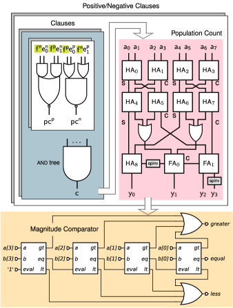
IV-C Magnitude Comparator
The magnitude comparator compares the number of votes from the positive and negative Tsetlin automaton teams. A larger number of positive votes indicates that the input pattern belongs to the class in question, and conversely, a larger number of negative votes indicates that the input pattern does not belong to the class in question.
The magnitude comparator is based on a request architecture [Wheeldon2019] and compares the operands in bit-pairs, starting from the most significant bit. Once a difference is found, the answer is known, and the remainder of the bits need not be compared. This architecture enables huge average-case latency improvement over a synchronous counterpart. Energy savings are also made by due to saved switching power on the lower bits when the operands differ by a large magnitude.
Since the comparator’s outputs (less, equal, and greater) are mutually exclusive, we take advantage of this in the asynchronous design. We use a 1-of-3 encoding on the output instead of the usual dual-rail—1-of-n encoding being a superset of dual-rail. Provided a spacer seperates the valids, the switching of 1-of-n codes is monotonic [Bainbridge2003], therefore satisfying Item 2. Without this trick, three sets of dual-rail signals would be required at the comparator outputa at the expense of more logic to drive these signals. The inputs to the comparator are dual-rail encoded.
IV-D Inference Datapath Results
| Technology | Design | Cell Area | Sequential Area | Avg. Power () | Leakage Power () | Avg. Latency () | Max Latency () | () | Avg. Inferences (Millions ) |
| UMC LL | Single-rail | — | |||||||
| Proposed Dual-rail | |||||||||
| Full Diffusion | Single-rail | — | |||||||
| Proposed Dual-rail |
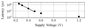
The inference datapath was synthesized using Synopsys Design Compiler for two different silicon libraries. UMC LL is a commercially available, low-leakage library which we use with nominal supply and TT corner. Full Diffusion is a custom library aimed at high performance subthreshold operation [Morris2017]. It uses a full diffusion sizing strategy with non-minimum-length transistors in order to mitigate subthreshold effects. For this silicon library the circuit is first synthesized at TT corner for nominal supply and results are shown with supply voltage in the range .
Results in Table I show similar cell areas for both single-rail and dual-rail designs for each silicon library. This is possible due to the careful choice of dual-rail circuit architecture and the reduced completion detection scheme. The dual-rail clause computation and magnitude comparator are more area efficient than their single-rail conterparts due to exploitation of dual-rail encoding and clever use of 1-of-3 encoding respectively.
For the area of the sequential cells we count flip-flop area for the single-rail designs and C-element area for dual-rail designs. The sequential area is similar between designs, despite the dual-rail design having twice as many sequential cells due to the doubled input rails. The dual-rail circuit uses C-elements as latches. These comprise four simple gates in the Full Diffusion library (due to lack of \textsmaller* gateAOI32 cells) and a single complex gate in the UMC LL library. Note that the cell area varies dramatically between the libraries due to transistor sizing—UMC LL being minimally-sized for superthreshold and Full Diffusion larger for subthreshold operation. The number of cells does not vary significantly.
Latency is measured from s\texorpdfstring to v in the dual-rail designs, and the clock period defines the latency for single-rail designs. The dual-rail circuit enables reduction in average latency thanks to early propagation. Average throughput is worsened however, due to the lengthened logic path and the need for the additional v\texorpdfstring to s transition. Although the dual-rail switching power is greater due to higher inherent activity factor, the computation energy is reduced due to increased throughput.
Throughput period is defined by the single-rail circuit’s clock period. For the dual-rail design, throughput period is determined by so that the [\AC@linebreakpenalty]PI are ready for the next operand. has the same magnitude as .
Figure 3 shows the effects of supply voltage on datapath latency. The latency increases exponentially as the supply voltage is reduced from . The key point is that the circuit functionality is guaranteed across the whole supply voltage range thanks to the requirements in Section III and without any alteration to the hardware.
V Conclusion
In this paper we have demonstrated an asynchronous, self-timed inference datapath design with area and power of equal orders of magnitude to the synchronous equivalent. Early propagation enables lower inference latency than the equivalent synchronous circuit on average. The savings are enabled by a reduced [\AC@linebreakpenalty]CD scheme which can be applied to any dual-rail asynchronous circuit. The new scheme introduces a timing assumption which can be incorporated into the [\AC@linebreakpenalty]CD circuit, so that the circuit environment does not need to be adapted. This type of low-latency circuit can have applications in speech recognition for wearables and other low-power applications where inference latency is of particular importance.
In future work we will apply asynchronous design styles to the training datapath of the [\AC@linebreakpenalty]TM algorithm in order to enable a fully-asynchronous [\AC@linebreakpenalty]ML hardware capable of on-chip learning.
- AI
- artificial intelligence
- BD
- bounded delay
- BNN
- binarized neural network
- CD
- completion detection
- CMOS
- complementary metal-oxide-semiconductor
- CNN
- convolutional neural network
- CTM
- convolutional Tsetlin machine
- CPOG
- conditional partial order graph
- DI
- delay insensitive
- DR
- dual-rail
- DRAM
- dynamic RAM
- DSP
- digital signal processing
- DVFS
- dynamic voltage and frequency scaling
- HDC
- hyperdimensional computing
- HDL
- hardware description language
- INWE
- inverse-narrow-width effect
- ISA
- instruction set architecture
- IoT
- internet of things
- LA
- learning automaton
- LEC
- logical equivalence checking
- LFSR
- linear feedback shift register
- LCG
- linear congruential generator
- LU
- learning unit
- MAC
- multiply-accumulate
- MEP
- minimum energy point
- ML
- machine learning
- MLP
- multi-layer perceptron
- MPP
- maximum power point
- MPPT
- maximum power point tracking
- NCL
- null convention logic
- NN
- neural network
- OCV
- on-chip variation
- PCG
- permuted congruential generator
- PI
- primary input
- PO
- primary output
- PRNG
- psuedorandom number generator
- PVT
- process, variation and temperature
- QDI
- quasi delay insensitive
- RAM
- random-access memory
- RCA
- ripple-carry adder
- RDF
- random dopant fluctuation
- RTL
- resistor-transistor logic
- RTM
- recurrent Tsetlin machine
- SCM
- standard cell memory
- SI
- speed independent
- SR
- single-rail
- SRAM
- static RAM
- STG
- signal transition graph
- STA
- static timing analysis
- SVM
- support vector machine
- TA
- Tsetlin automaton
- TAT
- Tsetlin automaton team
- TM
- Tsetlin machine
- TRNG
- true random number generator
- ULV
- ultra-low voltage
- VLSI
- very-large-scale integration
- WSN
- wide sensor network