Nanoscopic charge fluctuations in a gallium phosphide waveguide
measured by single molecules
Abstract
We present efficient coupling of single organic molecules to a gallium phosphide subwavelength waveguide (nanoguide). By examining and correlating the temporal dynamics of various single-molecule resonances at different locations along the nanoguide, we reveal light-induced fluctuations of their Stark shifts. Our observations are consistent with the predictions of a simple model based on the optical activation of a small number of charges in the GaP nanostructure.
* A.S. and D.R. contributed equally to this work.
One of the promising platforms for future quantum technologies is based on integrated nanophotonics, where a large number of quantum emitters and quantum states of light are efficiently interconnected via a labyrinth of subwavelength waveguides (nanoguides) and other nano-optical elements Wang et al. (2020); Kim et al. (2020); Elshaari et al. (2020); Sandoghdar (2020); Türschmann et al. (2019). The optimal choice of materials for achieving this goal has not been settled yet, but semiconductors (e.g., GaAs) Thyrrestrup et al. (2018); Hallett et al. (2018); Grim et al. (2019) and diamond Atatüre et al. (2018) architectures have made significant progress. In most cases, quantum emitters have been situated inside the host material of the nanoguides, e.g., AlGaAs quantum dots in GaAs or color centers in diamond. To decouple the choices of ideal quantum emitters, appropriate guiding architectures, and other nano-optical elements from each other, there is a large effort towards hybrid solutions Akimov et al. (2007); Türschmann et al. (2017); Lombardi et al. (2018); Grandi et al. (2019); Hail et al. (2019); Fröch et al. (2020); Elshaari et al. (2020); Kim et al. (2020).
Guiding light on a chip is best realized in a material with high refractive index, . Common choices for waveguides in the visible and near-infrared regimes have been silicon nitride Lombardi et al. (2018); Wan et al. (2020); Fröch et al. (2020) or titanium dioxide Türschmann et al. (2017); Rattenbacher et al. (2019) with . Semiconductors such as Si and GaAs offer considerably larger but at the expense of strong absorption for wavelengths smaller than . Gallium phosophide (GaP) presents a very attractive alternative with and a cutoff wavelength below Barclay et al. (2009); Wolters et al. (2010); Gould et al. (2016); Wilson et al. (2020), and indeed, recent efforts have established fabrication of high-quality nanophotonic chips from this material on Hönl et al. (2018); Schneider et al. (2018). In this work, we show efficient coupling of single organic molecules to a GaP nanoguide. Furthermore, we investigate light-induced charge fluctuations in the nanoguide by analyzing the spatio-temporal features of single-molecule Stark shifts.
Efficient coupling of molecules to a GaP nanoguide. The core of our experimental platform is a long GaP nanoguide fabricated on a thick layer on a silicon substrate Hönl et al. (2018); Schneider et al. (2018). The nanoguide has a cross-section of , is terminated on both sides by grating couplers and is decorated by sawtooth-shaped gold microelectrodes placed from the nanoguide (see Fig. 1(a, b)). The nanoguide supports two propagating modes of orthogonal polarization states, which have the majority of their energy concentrated in the evanescent field (see Fig. 1(b)). Fabrication details are presented in earlier works Hönl et al. (2018); Schneider et al. (2018); Wilson et al. (2020).
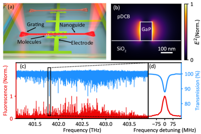
The nanostructures are covered by a para-dichlorobenzene (pDCB) crystal confined in a nanochannel as described in previous publications Gmeiner et al. (2016); Türschmann et al. (2017); Rattenbacher et al. (2019). By doping the pDCB crystal with dibenzoterrylene (DBT) at a concentration of mol/mol, we realize a random distribution of the latter. At a temperature below , DBT molecules possess strong zero-phonon lines with a lifetime-limited linewidth of at a vacuum transition wavelength of (frequency of ) Nicolet et al. (2007); Verhart et al. (2014). Owing to variations in their nanoscopic crystal environment Gmeiner et al. (2016), the resonance frequencies of individual molecules span a range of about (). The transverse electric (TE) mode of the nanoguide (see Fig. 1(b)) is excited by continuous-wave Ti:Sapphire laser beams (linewidth ), and the outcoupled radiation is detected on an avalanche photodiode. The blue curve in Fig. 1(c) displays the extinction spectra of several hundred molecules measured in transmission, while the red spectrum reports on the corresponding fluorescence via the vibrational levels of the ground state and phonon wings. In Fig. 1(d), we plot a closeup for a single-molecule extinction dip of 13%, comparable with the coupling efficiency achieved for illumination in a diffraction-limited focus spot Wrigge et al. (2008).
Monitoring the local electric field. The molecule DBT has inversion symmetry and is thus expected to undergo a quadratic Stark shift. Figure 2(a) illustrates the parabolic spectra of three nanoguide-coupled molecules as a function of the voltage applied to the nearby electrodes. In some cases, local strain in the matrix leads to the addition of a linear Stark effect manifested by an offset in the turning points of the parabolas Orrit et al. (1992); Moradi et al. (2019). A more noteworthy observation in these spectra is, however, that the resonances appear broader and less stable at larger slopes of the Stark tuning profile (see e.g., the spectra across the dashed line in Fig. 2(a)). We point out that this effect is consistently observed for all nanoguide-coupled molecules on all studied GaP samples. On the contrary, we have verified that molecules at about away from the nanoguide are highly stable and have a lifetime-limited linewidth regardless of the applied Stark shift. For the latter measurements, we shined a focused laser beam normal to the plane of the chip.
We, thus, attribute the origin of the spectral instabilities for nanoguide-coupled molecules to electric field fluctuations originating from the GaP nanostructure. As we show in the following, the effect at hand is very different from previous reports of electric field-induced spectral instability and broadening of organic molecules, which were caused by two-level tunneling systems Phillips (1972); Heuer and Silbey (1993); Maier et al. (1995); Segura et al. (2001); Bauer and Kador (2003); Gerhardt et al. (2009) or electro-mechanical oscillations Tian et al. (2014) in the host organic matrix.
To investigate the temporal dynamics of the spectral instabilities more quantitatively, we increased the frequency scan rate from in Fig. 2(a) to . This was sufficient to arrive at lifetime-limited Lorentzian resonances in individual frequency sweeps and, thus, resolve the wandering of their center frequencies over time. To characterize Stark spectra such as those shown in Fig. 2(a), we recorded a large number of individual scans. In this manner, we obtained a robust mean value () for the molecular resonance frequency and root mean square (RMS) frequency fluctuations () at a given electrode voltage (). By repeating this procedure for many applied voltages, we established the frequency tunability defined as . Figures 2(b) and 2(c) display examples of spectral trajectories of a molecule, which we name M1, at two applied voltages.
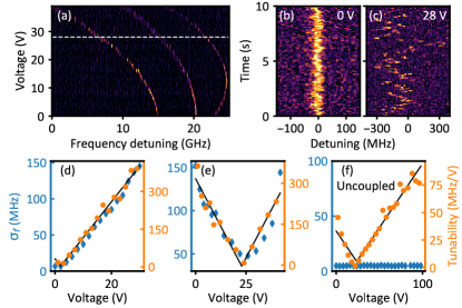
Figure 2(d-f) shows and the tunability for three exemplary molecules. For M1, (orange) increases linearly with , as shown in Fig. 2(d), implying a quadratic Stark behavior. Interestingly, (blue) also grows proportionally with . Figure 2(e) presents the case of a second nanoguide-coupled molecule that behaves similarly although its turning point () is shifted to a voltage of about . As a control experiment, in Fig. 2(f) we report on a molecule far away from the nanoguide. It is evident that, in this case, there is no correlation between and , which stays at 4 MHz, given by the fit error.
Assuming that the field fluctuations originate from the nanoguide, we express the total Stark shift experienced by the molecule as , where , and denote the fields created by the residual strain in the crystal, the electrodes, and the nanoguide, respectively. A cross term in this expression leads to the amplification of a small fluctuating by a large constant . The former quantity causes while the latter dictates such that becomes proportional to , as observed in our measurements. The measured data in Fig. 2(e, d) and our knowledge of the electrode and nanoguide geometries let us deduce the RMS nanoguide field fluctuations to be around at the position of the molecule. This corresponds to the field generated by a single electron at a distance of , which is comparable to the typical separation of the evanescently-coupled nanoguide-molecule system.
Temporal field correlations. The ability to scan faster than typical electric field fluctuations allows us to determine the correlation function between the frequency fluctuations of molecules and . Figure 3(a) plots the autocorrelation function computed for molecule M1 from 12,000 individual sweeps, 100 of which are displayed in Fig. 3(b). By fitting an exponential function to , we extract the autocorrelation time .
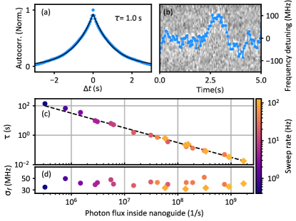
Next, we studied the dependence of and on the optical power () in the nanoguide. Figure 3(c, d) displays the outcome of measurements for one molecule, indicating an inverse proportionality relation between and over four orders of magnitude. This robust dependency clearly demonstrates that the fluctuations are photo-induced. We checked that the observed phenomenon is not caused by direct interaction of light with the molecule. To do this, we performed measurements, where up to 90% of the optical power inside the nanoguide was provided by a second laser beam detuned by 2 THz from the molecule and verified that the fluctuation rate () scaled with the total laser power in the nanoguide. Furthermore, we found that remains independent of within our measurement precision (see Fig. 3(d)). This indicates that while the external illumination power dictates the spectral noise dynamics, it does not influence its amplitude.
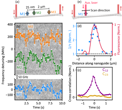
Spatial field correlations. We now investigate the spatial properties of the observed electric field noise by simultaneous measurement of several molecules. Here, we coupled two independent laser beams into the nanoguide and performed time-multiplexed alternate frequency sweeps in two different frequency regions. In Fig. 4, we present an example, where the frequency fluctuations of three molecules (M1, M2 and M3; see Fig. 4(a)) were examined. The frequency variations and the cross-correlation functions displayed in Figs. 4(b) and 4(c), respectively, reveal that the spectral fluctuations in M1 and M2 are correlated, but M3 behaves independently. Considering the error in extracting resonance frequencies, we infer almost perfect correlation between M1 and M2. By determining the positions of each molecule through localization microscopy, we revealed that, indeed, M1 and M2 were separated by only nm, while M3 was about away from them. For another correlated pair separated by about we saw that the peak spectral cross-correlation drops to , verifying that the field fluctuations are very local.
To provide further evidence for the local character of the field fluctuations, we also conducted single-molecule measurements under illumination by an auxiliary laser beam that was frequency detuned by 6 GHz. Here, we scanned the focal spot of this second beam along the nanoguide across the molecule position (see Fig. 4(d,e)) and recorded changes in . The blue symbols in Fig. 4(d) confirm that follows the intensity profile of the auxiliary light beam shown by the red curve (full width at half-maximum )
Theoretical modelling. Regardless of the details of the process at work, electric field fluctuations generated by the nanoguide can be attributed to charge fluctuations. Redistribution of charges in semiconductors can be caused by many effects such as trapped or wandering charges Müller et al. (2005); Sallen et al. (2011); Bardoux et al. (2006); Wolters et al. (2013); Thoma et al. (2016); Liu et al. (2018), impurities Hauck et al. (2014), or ligand rearrangements Fernée et al. (2012); Beyler et al. (2013) and have also been shown to be driven by light with energy below the bandgap Tomm (2016). We consider a simple model in which electric field fluctuations result from the rearrangement of randomly distributed point charges with density in the GaP nanoguide. We assume that each charge stays in the vicinity of its original position, but it experiences an average displacement upon scattering one photon. In other words, while the field fluctuation rate scales with the optical power , and remain independent of it. It can then be shown that . Furthermore, the randomness of the jumps and the quadratic fall-off of the Coulomb field lead to a short correlation length, approximately equal to the molecule-waveguide distance.
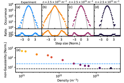
In the limit of large , one expects a Gaussian statistics for the frequency steps. The upper panel of Fig. 5(a) shows that the histogram of the measured data clearly deviates from a Gaussian distribution shown in grey. To compare the statistical properties of the frequency fluctuations with the predictions of our model, we simulated time traces of the molecular resonance frequencies for different values and used the same analysis procedure applied to the experimental data to generate a histogram of the frequency steps. The upper panel of Fig. 5(b-d) displays the outcome for three synthetic data sets. It turns out that at the lowest considered density, corresponding to the effect of only charges, the molecular resonance experiences jump-like frequency shifts, causing a non-Gaussian frequency step-size distribution.
To quantify the deviations from a Gaussian distribution, we consider the ratio of the occurrence to the corresponding Gaussian fit distribution as plotted in the lower panel of Fig. 5(a-d). Next, as presented in Fig. 5(e), we introduce a measure of non-Gaussianity (), defined as the area under this curve above one. The experimentally measured marked by the blue line corresponds to a density of charges around , or equivalently to about one charge per . Although this analysis only established an estimate, the result is in agreement with the typical density of defects, impurities or charge traps seen in such systems Hauck et al. (2014) and implies that an average of 50 charges govern the frequency fluctuations of our molecules. Given this density and the experimentally measured magnitude of the frequency fluctuations, we can estimate . We also note that owing to the small width of the nanoguide, surface and volume charges lead to similar results.
Conclusions. We have used single molecules as nanometer-sized probes for investigating the spatio-temporal behavior of a low number of charges activated in GaP nanoguides. The small size, excellent spectral properties, large achievable concentrations and the inhomogeneous distribution of their resonance frequencies make organic molecules a promising tool for ultrasensitive characterization of nanoscopic charge dynamics in a range of systems such as single electron transistors, quantum dots or superconductors Rezai et al. (2018); Caruge and Orrit (2001); Fauré et al. (2007); Vamivakas et al. (2011); Arnold et al. (2014); Faez et al. (2014). Our findings also advance the use of GaP as a platform for integrated quantum photonics Wilson et al. (2020); Sandoghdar (2020); Wang et al. (2020); Kim et al. (2020). The observed light-induced field fluctuations are small and slow enough to be tolerated or eliminated by more sophisticated fabrication schemes Guha et al. (2017); Liu et al. (2018). However, even in their current form, the estimated density of charges and their light absorption probability signified by the slope of Fig. 3(c) point to a loss coefficient of about , which would allow for resonator quality factors in the order of .
Acknowledgment. We acknowledge financial support by the Max Planck Society as well as the RouTe Project (13N14839) through the Federal Ministry of Education and Research (BMBF) and the European Union’s Horizon 2020 Program for Research and Innovation under grants 722923 (Marie Curie H2020-ETN OMT) and 732894 (FET Proactive HOT). A.S. acknowledges support through an Alexander von Humboldt fellowship.
References
- Wang et al. (2020) J. Wang, F. Sciarrino, A. Laing, and M. G. Thompson, Nat. Photonics 14, 273 (2020).
- Kim et al. (2020) J.-H. Kim, S. Aghaeimeibodi, J. Carolan, D. Englund, and E. Waks, Optica 7, 291 (2020).
- Elshaari et al. (2020) A. W. Elshaari, W. Pernice, K. Srinivasan, O. Benson, and V. Zwiller, Nat. Photonics 14, 285 (2020).
- Sandoghdar (2020) V. Sandoghdar, Nano Lett. 20, 4721 (2020).
- Türschmann et al. (2019) P. Türschmann, H. L. Jeannic, S. F. Simonsen, H. R. Haakh, S. Götzinger, V. Sandoghdar, P. Lodahl, and N. Rotenberg, Nanophotonics 8, 1641 (2019).
- Thyrrestrup et al. (2018) H. Thyrrestrup, G. Kiršanskė, H. Le Jeannic, T. Pregnolato, L. Zhai, L. Raahauge, L. Midolo, N. Rotenberg, A. Javadi, R. Schott, A. D. Wieck, A. Ludwig, M. C. Löbl, I. Söllner, R. J. Warburton, and P. Lodahl, Nano Lett. 18, 1801 (2018).
- Hallett et al. (2018) D. Hallett, A. P. Foster, D. L. Hurst, B. Royall, P. Kok, E. Clarke, I. E. Itskevich, A. M. Fox, M. S. Skolnick, and L. R. Wilson, Optica 5, 644 (2018).
- Grim et al. (2019) J. Q. Grim, A. S. Bracker, M. Zalalutdinov, S. G. Carter, A. C. Kozen, M. Kim, C. S. Kim, J. T. Mlack, M. Yakes, B. Lee, and D. Gammon, Nature Materials 18, 963 (2019).
- Atatüre et al. (2018) M. Atatüre, D. Englund, N. Vamivakas, S.-Y. Lee, and J. Wrachtrup, Nat. Rev. Mater. 3, 38 (2018).
- Akimov et al. (2007) A. V. Akimov, A. Mukherjee, C. L. Yu, D. E. Chang, A. S. Zibrov, P. R. Hemmer, H. Park, and M. D. Lukin, Nature 450, 402 (2007).
- Türschmann et al. (2017) P. Türschmann, N. Rotenberg, J. Renger, I. Harder, O. Lohse, T. Utikal, S. Götzinger, and V. Sandoghdar, Nano Lett. 17, 4941 (2017).
- Lombardi et al. (2018) P. Lombardi, A. P. Ovvyan, S. Pazzagli, G. Mazzamuto, G. Kewes, O. Neitzke, N. Gruhler, O. Benson, W. H. P. Pernice, F. S. Cataliotti, and C. Toninelli, ACS Photonics 5, 126 (2018).
- Grandi et al. (2019) S. Grandi, M. P. Nielsen, J. Cambiasso, S. Boissier, K. D. Major, C. Reardon, T. F. Krauss, R. F. Oulton, E. A. Hinds, and A. S. Clark, APL Photonics 4, 086101 (2019).
- Hail et al. (2019) C. U. Hail, C. Höller, K. Matsuzaki, P. Rohner, J. Renger, V. Sandoghdar, D. Poulikakos, and H. Eghlidi, Nat. Com. 10, 1880 (2019).
- Fröch et al. (2020) J. E. Fröch, S. Kim, N. Mendelson, M. Kianinia, M. Toth, and I. Aharonovich, ACS Nano 14, 7085 (2020).
- Wan et al. (2020) N. H. Wan, T.-J. Lu, K. C. Chen, M. P. Walsh, M. E. Trusheim, L. De Santis, E. A. Bersin, I. B. Harris, S. L. Mouradian, I. R. Christen, E. S. Bielejec, and D. Englund, Nature 583, 226 (2020).
- Rattenbacher et al. (2019) D. Rattenbacher, A. Shkarin, J. Renger, T. Utikal, S. Götzinger, and V. Sandoghdar, New J. Phys. 21, 062002 (2019).
- Barclay et al. (2009) P. E. Barclay, K.-M. C. Fu, C. Santori, and R. G. Beausoleil, Applied Physics Letters 95, 191115 (2009).
- Wolters et al. (2010) J. Wolters, A. W. Schell, G. Kewes, N. Nüsse, M. Schoengen, H. Döscher, T. Hannappel, B. Löchel, M. Barth, and O. Benson, Applied Physics Letters 97, 141108 (2010).
- Gould et al. (2016) M. Gould, E. R. Schmidgall, S. Dadgostar, F. Hatami, and K.-M. C. Fu, Phys. Rev. Applied 6, 011001 (2016).
- Wilson et al. (2020) D. J. Wilson, K. Schneider, S. Hönl, M. Anderson, Y. Baumgartner, L. Czornomaz, T. J. Kippenberg, and P. Seidler, Nat. Photonics 14, 57 (2020).
- Hönl et al. (2018) S. Hönl, H. Hahn, Y. Baumgartner, L. Czornomaz, and P. Seidler, J. Phys. D: Appl. Phys. 51, 185203 (2018).
- Schneider et al. (2018) K. Schneider, P. Welter, Y. Baumgartner, H. Hahn, L. Czornomaz, and P. Seidler, J. Lightwave Technol. 36, 2994 (2018).
- Gmeiner et al. (2016) B. Gmeiner, A. Maser, T. Utikal, S. Götzinger, and V. Sandoghdar, Phys. Chem. Chem. Phys. 18, 19588 (2016).
- Nicolet et al. (2007) A. A. L. Nicolet, P. Bordat, C. Hofmann, M. A. Kol’chenko, B. Kozankiewicz, R. Brown, and M. Orrit, ChemPhysChem 8, 1929 (2007).
- Verhart et al. (2014) N. R. Verhart, G. Lepert, A. L. Billing, J. Hwang, and E. A. Hinds, Opt. Express 22, 19633 (2014).
- Wrigge et al. (2008) G. Wrigge, I. Gerhardt, J. Hwang, G. Zumofen, and V. Sandoghdar, Nature Phys. 4, 60 (2008).
- Orrit et al. (1992) M. Orrit, J. Bernard, A. Zumbusch, and R. Personov, Chem. Phys. Lett. 196, 595 (1992).
- Moradi et al. (2019) A. Moradi, Z. Ristanović, M. Orrit, I. Deperasińska, and B. Kozankiewicz, ChemPhysChem 20, 55 (2019).
- Phillips (1972) W. A. Phillips, J. Low Temp. Phys. 7, 351 (1972).
- Heuer and Silbey (1993) A. Heuer and R. J. Silbey, Phys. Rev. Lett. 70, 3911 (1993).
- Maier et al. (1995) H. Maier, R. Wunderlich, D. Haarer, B. M. Kharlamov, and S. G. Kulikov, Phys. Rev. Lett. 74, 5252 (1995).
- Segura et al. (2001) J.-M. Segura, G. Zumofen, A. Renn, B. Hecht, and U. Wild, Chem. Phys. Lett. 340, 77 (2001).
- Bauer and Kador (2003) M. Bauer and L. Kador, J. Chem. Phys. 118, 9069 (2003).
- Gerhardt et al. (2009) I. Gerhardt, G. Wrigge, and V. Sandoghdar, Mol. Phys. 107, 1975 (2009).
- Tian et al. (2014) Y. Tian, P. Navarro, and M. Orrit, Phys. Rev. Lett. 113, 135505 (2014).
- Müller et al. (2005) J. Müller, J. M. Lupton, A. L. Rogach, J. Feldmann, D. V. Talapin, and H. Weller, Phys. Rev. B 72, 205339 (2005).
- Sallen et al. (2011) G. Sallen, A. Tribu, T. Aichele, R. André, L. Besombes, C. Bougerol, M. Richard, S. Tatarenko, K. Kheng, and J. P. Poizat, Phys. Rev. B 84, 1 (2011).
- Bardoux et al. (2006) R. Bardoux, T. Guillet, P. Lefebvre, T. Taliercio, T. Bretagnon, S. Rousset, B. Gil, and F. Semond, Phys. Rev. B 74, 195319 (2006).
- Wolters et al. (2013) J. Wolters, N. Sadzak, A. W. Schell, T. Schröder, and O. Benson, Phys. Rev. Lett. 110, 027401 (2013).
- Thoma et al. (2016) A. Thoma, P. Schnauber, M. Gschrey, M. Seifried, J. Wolters, J.-H. Schulze, A. Strittmatter, S. Rodt, A. Carmele, A. Knorr, T. Heindel, and S. Reitzenstein, Phys. Rev. Lett. 116, 033601 (2016).
- Liu et al. (2018) J. Liu, K. Konthasinghe, M. Davanço, J. Lawall, V. Anant, V. Verma, R. Mirin, S. W. Nam, J. D. Song, B. Ma, Z. S. Chen, H. Q. Ni, Z. C. Niu, and K. Srinivasan, Phys. Rev. Applied 9, 064019 (2018).
- Hauck et al. (2014) M. Hauck, F. Seilmeier, S. E. Beavan, A. Badolato, P. M. Petroff, and A. Högele, Phys. Rev. B 90, 235306 (2014).
- Fernée et al. (2012) M. J. Fernée, T. Plakhotnik, Y. Louyer, B. N. Littleton, C. Potzner, P. Tamarat, P. Mulvaney, and B. Lounis, J. Phys. Chem. Lett. 3, 1716 (2012).
- Beyler et al. (2013) A. P. Beyler, L. F. Marshall, J. Cui, X. Brokmann, and M. G. Bawendi, Phys. Rev. Lett. 111, 177401 (2013).
- Tomm (2016) J. J. W. Tomm, Spectroscopic Analysis of Optoelectronic Semiconductors (Springer, 2016).
- Rezai et al. (2018) M. Rezai, J. Wrachtrup, and I. Gerhardt, Phys. Rev. X 8, 031026 (2018).
- Caruge and Orrit (2001) J. M. Caruge and M. Orrit, Phys. Rev. B 64, 1 (2001).
- Fauré et al. (2007) M. Fauré, B. Lounis, and A. I. Buzdin, EPL 77, 17005 (2007).
- Vamivakas et al. (2011) A. N. Vamivakas, Y. Zhao, S. Fält, A. Badolato, J. M. Taylor, and M. Atatüre, Phys. Rev. Lett. 107, 1 (2011).
- Arnold et al. (2014) C. Arnold, V. Loo, A. Lemaître, I. Sagnes, O. Krebs, P. Voisin, P. Senellart, and L. Lanco, Phys. Rev. X 4, 1 (2014).
- Faez et al. (2014) S. Faez, S. J. van der Molen, and M. Orrit, Phys. Rev. B 90, 205405 (2014).
- Guha et al. (2017) B. Guha, F. Marsault, F. Cadiz, L. Morgenroth, V. Ulin, V. Berkovitz, A. Lemaître, C. Gomez, A. Amo, S. Combrié, B. Gérard, G. Leo, and I. Favero, Optica 4, 218 (2017).