Molecular beam epitaxy growth of the highly conductive oxide SrMoO3
Abstract
SrMoO3 is a promising material for its excellent electrical conductivity, but growing high-quality thin films remains a challenge. Here we synthesized epitaxial films of SrMoO3 using molecular beam epitaxy (MBE) technique under low oxygen-flow rate. Introduction of SrTiO3 buffer layers of 4–8 unit cells between the film and the (001)-oriented SrTiO3 or KTaO3 substrate was crucial to remove impurities and/or roughness of the film surface. The obtained film shows improved electrical conductivities as compared with films obtained by other techniques. The high quality of the SrMoO3 film is also verified by angle resolved photoemission spectroscopy (ARPES) measurements showing a clear Fermi surfaces.
I Introduction
Perovskite oxides with a general formula O3 exhibit various intriguing properties such as ferroelectricity, piezoelectricity, ion conductivity, colossal magnetoresistance, and superconductivity Tilley (2016). SrMoO3 is a Pauli paramagnetic metal with excellent electrical conductivity Brixner (1960); Nagai et al. (2005). The room temperature (RT) resistivity of single-crystalline SrMoO3 is as low as 5 cm, which is much lower than typical oxide materials Mackenzie (2017) and is rather close to those of nearly free electron systems such as sodium and copper. The utmost feature of this oxide has stimulated intensive studies to grow epitaxial films Inukai and Murakami (1985); Mizoguchi et al. (2000); Wanga et al. (2001); Radetinac et al. (2010, 2014) for applications, for example, electrodes between oxide interfaces Inukai and Murakami (1985); Salg et al. (2019) and transparent conductors Mizoguchi et al. (2000); Radetinac et al. (2016). Unfortunately, all the films, so far prepared by pulsed laser deposition (PLD) Wanga et al. (2001); Radetinac et al. (2010, 2014); Salg et al. (2019); Radetinac et al. (2016); Wadati et al. (2014) or sputtering Inukai and Murakami (1985); Mizoguchi et al. (2000), show rather poor resistivity (27–150 cm) than that of the bulk single crystal, possibly due to the presence of defects or inclusion of impurity phases. It is notable that an insulating Mo6+ phase is often found in the surface state Salg et al. (2019); Radetinac et al. (2016); Wadati et al. (2014).
Among available techniques of thin film preparation, molecular beam epitaxy (MBE) is known as a method that allows the growth of thin films with high quality Schlom (2015). This is because much smaller kinetic energy of constituent elements supplied in this process Oka and Fukumura (2017) provides an almost thermal equilibrium condition, avoiding an undesired oxide off-stoichiometry. For this reason, we have employed the MBE method, for the first time, to grow SrMoO3 films, using elemental Sr and Mo as fluxes. By optimizing growth conditions such as O2 flow rate, we have successfully obtained epitaxial thin film of SrMoO3. In particular, the use of a SrTiO3 buffer layer between the SrMoO3 film and the substrate is found to be crucial to obtain high quality films with less impurities and/or roughness in the surface. The high-quality of the film is verified by X-ray diffraction (XRD) and angle resolved photoemission spectroscopy (ARPES) measurements. The film with the SrTiO3 buffer layer exhibited an improved resistivity of 24 cm at RT as compared with the SrMoO3 films by other techniques Inukai and Murakami (1985); Wanga et al. (2001); Radetinac et al. (2010, 2014, 2016); Wang et al. (2001); not (a).
II Experimental section
Films of SrMoO3 were grown on the (001)-oriented SrTiO3 (STO) or KTaO3 (KTO) substrates with a custom-made reactive MBE system (EGL-1420-E2, Biemtron). Elemental Sr and Mo fluxes were simultaneously provided from a conventional Knudsen cell and electron beam evaporation system. Typical flux rates were 0.04 Å/s for Sr and 0.01 Å/s for Mo, as determined by an INFICON quartz crystal microbalance system before growth. The growth temperature window was 450–600 ∘C, which was monitored by an optical pyrometer. The optimal growth temperature was found to be 520 ∘C. We flowed O2 gas at a rate of 0.1 sccm, which gives a background pressure of about Torr. Lower quality SrMoO3 films were obtained under a higher oxygen pressure, while under ozone flow, SrMoO3 was not obtained. The surface structure of the film and substrate was monitored in-situ by reflection high-energy electron diffraction (RHEED) with an acceleration voltage of 20 keV.
X-ray diffraction (XRD) measurements after the growth were carried out at RT with a Rigaku SmartLab diffractometer equipped with a Cu K monochromator.
The electrical resistivity was measured by using a standard four-probe method. Au/Ti metal electrodes were vacuum-evaporated on the films for electrical contacts, and gold wires ( m) were attached with silver paste to these electrodes.
Soft x-ray photoemission measurements were performed at K with a synchrotron-radiation photoemission spectroscopy system at Photon Factory BL-2. The film used in these measurements was deposited after the growth of a STO buffer layer on the Nb-doped (001)-STO substrate to eliminate the charging effect. The thickness of the SrMoO3 film used in experiments was 14.6 nm. The top of the film was capped with one unit cell of STO to protect the SrMoO3-film surface from further oxidation. Thus no surface cleaning was conducted. ARPES was performed for the same sample. The position of Fermi energy was determined by measuring the spectra of gold which was electrically connected to the sample.
For the theoretical reference of ARPES results, electronic structures were calculated using the QUANTUM ESPRESSO package Giannozzi et al. (2009, 2017). We used projector-augmented wave pseudopotentials Kresse and Joubert (1999) and the Perdew-Burke-Ernzerhof parameterization of the generalized gradient approximation Perdew et al. (1996). The cutoff energies in the wave function and charge densities were 80 and 500 Ry, respectively. A k-mesh in the first Brillouin zone was used. It is worth noting that the bulk SrMoO3 exhibits structural transitions, upon heating, from an orthorhombic phase to a tetragonal phase at K, and to a cubic phase at 250 K Macquart et al. (2010). However, the distortion from the cubic symmetry is subtle and does not largely alter its band structure Wadati et al. (2014). Our band structure calculations also confirmed this result. We will show the result for the cubic SrMoO3 unless otherwise specified.
III Results and discussion
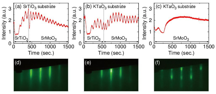
For the growth of high quality SrMoO3 films, we used a buffer layer of STO with 4-8 unit cells, between the SrMoO3 film and the STO (or KTO) substrate. Such buffer layer has been used for the growth of SrMoO3 and EuMoO3 by PLD Radetinac et al. (2014); Salg et al. (2019); Kozuka et al. (2012). In this study, we firstly deposited SrTiO3 using Sr and Ti under O2 gas flow, and then we started the growth of SrMoO3 films at the peak top of oscillation in RHEED for SrTiO3 (Figs. 1(a) and (b)). The interval between each peak corresponds to one unit cell of SrMoO3 (or SrTiO3) Terashima et al. (1990). For substrates of SrTiO3 and Nb-doped SrTiO3, the oscillation amplitude gradually reduced after the growth of 10–15 unit cells of SrMoO3 (Fig. 1(a)), while it retained almost constant in the case of the KTaO3 substrate (Fig. 1(b)). For comparison, we present RHEED intensity profiles during the growth of the SrMoO3 film on the non-buffered KTO substrate (Fig. 1(c)). It is seen that the RHEED intensity oscillation soon disappears when no buffer is used (Fig. 1(c)). The growth of 25–40 unit cells of SrMoO3 (10–16 nm) was checked by the RHEED intensity oscillations or estimating time with the average interval of oscillation peaks or with the growth rates. Figures 1(d)–(f) display RHEED patterns at the end of the growth for the same samples in Figs.1(a)–(c), respectively. Streaky RHEED patterns ensure flat surface of the films (Figs.1(d)–(e)), while the spot-like (or slightly modulated) features are observed along with original streaks for the film without the buffer layer (Fig.1(f)), suggesting roughening of the film surface Has . We also used the so-called STEP substrate of SrTiO3 with 100% TiO2-terminated surface, but epitaxial growth was not possible in the current growth condition. The difference between the presence and absence of the buffer layer for the electrical conductance will be discussed in a later section.
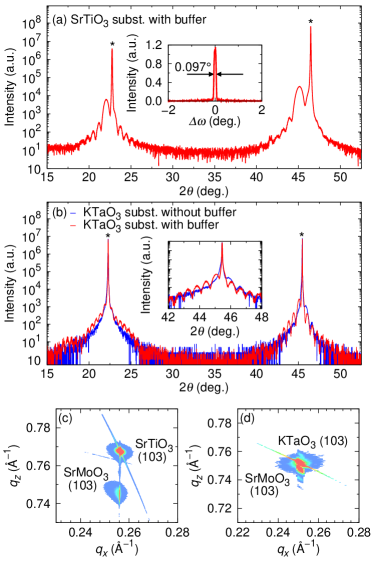
Figures 2(a)–(b) show the out-of-plane – XRD patterns for the same samples in Figs. 1(a)–(c). Sharp peaks with distinct fringes are observed around and 45∘ for the SrMoO3 film on the STO-buffered STO (S-STO) substrate (Fig. 2(a)), indicating excellent orientation and atomic scale smoothness of the interface between the substrate and the film. A similar tendency of the XRD profile and fringes is observed in the films on the STO-buffered KTO (S-KTO) and non-buffered substrates (Fig. 2(b)), where the XRD peaks of the films are overlapped with those of the KTO substrates. It is seen that fringes of the XRD spectrum of the SrMoO3 film on the non-buffered KTO substrate are weakened (the inset of Fig. 2(b)), implying poorer quality of the film interface with the substrate. This result is consistent with the RHEED observation (Fig.1(f)), suggesting island growth and its coalescence accompanied by the generation of grain boundaries and/or impurities Freund and Suresh (2003). The film thickness estimated from the spacing of fringes is 11.3 nm, 15.6 nm, and 16 nm for the films on the S-STO, S-KTO, and non-buffered KTO substrates, respectively. These values agree with the thickness estimated from the interval of RHEED oscillation peak and time as well as the growth rate. The rocking curve of the XRD peak around the 001 peak for the film on the STO substrate () is (inset of Fig. 2(a)). This value is slightly broader than that of SrMoO3 films on the GdScO3 substrate with PLD Radetinac et al. (2010, 2014), which is probably because our film is thinner. An alternate possibility is a lattice mismatch between the bulk SrMoO3 ( Å) and SrTiO3 ( Å), leading to a strain effect. In fact, a pseudocubic lattice constant of GdScO3 ( Å) Schubert et al. (2003) is closer to that of bulk cubic SrMoO3. The rocking curve of the (00) peaks of the SrMoO3 films on the KTO substrates was not measured due to the fact that the sample peaks are overlapped with the substrate peaks. Figure 2(c) and (d) show the reciprocal space mappings around the 103 peak of SrMoO3 for the film on the S-STO and S-KTO substrates. The 103 peaks of the films are located near the same value of the 103 peaks of the substrates, indicating a coherent growth of the target film, with an in-plane lattice parameter almost identical to that of the substrate. The lattice parameters of the SrMoO3 film on the S-STO substrate are Å, and Å, meaning that the cell volume is reduced by about 3% relative to the bulk sample Macquart et al. (2010). The reduced/expanded / axis is reasonable given the compressive strain from the SrTiO3 substrate. The lattice parameters of the SrMoO3 film on the S-KTO substrate are Å (in-plane) and Å (out of plane). The overall lattice expansion of the film about 1% in volume with respect to bulk SrMoO3 may result from the tensile substrate strain which could also induces oxygen vacancies Aschauer et al. (2013).
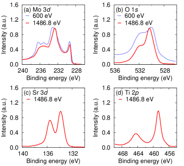
Core-level photoemission spectrum of the SrMoO3 film provided evidence for the Mo4+ state associated with two sharp peaks at the binding energy of 229.3 eV and 232.6 eV for the photon energy of 1486.8 eV (Fig. 3(a)). A broad satellite was also observed next to the sharp peaks, which is likely Mo4+ 3d emission of unscreened final states Radetinac et al. (2014); Salg et al. (2019); Colton et al. (1978); Scanlon et al. (2010). We also collected a spectrum at a lower photon energy (600 eV), which is more sensitive for the film near the surface, and observed additional features at 233.1 eV and 236.4 eV. These peaks are attributed to Mo6+ 3d emissions as observed in MoO3 Colton et al. (1978); Scanlon et al. (2010); Wadati et al. (2014), suggesting the oxidation of Mo around the interface with the topmost capping layer of STO ( nm). Note that the broad feature at about 235 eV cannot readily be explained by a simple component of Mo states; it may be due to plasmon satellite as discussed by Wadati et al. Wadati et al. (2014). The interface oxidations were also confirmed by O 1s spectra (Fig. 3(b)), with two prominent features at 530.2 eV and 532 eV. Since the contribution from the STO capping layer is expected to be about 20% for eV not (b), this additional 532 eV peak mainly comes from Mo6+ containing impurities around the SrMoO3 film. The relative intensity at 532 eV (vs. 530.2 eV) increases when the photon energy of 600 eV is used. No influence of oxidation is seen in the Sr 3d spectrum with peaks for the Sr2+ state (Fig. 3(c)), implying the composition of Sr2+Mo4+O3 in the most part of the film. The peak positions of the Ti 2p spectrum from the STO capping layer are in good agreement with reported data Radetinac et al. (2014); Wagner et al. (1979), though the spectrum is slightly broader (Fig. 3(d)).
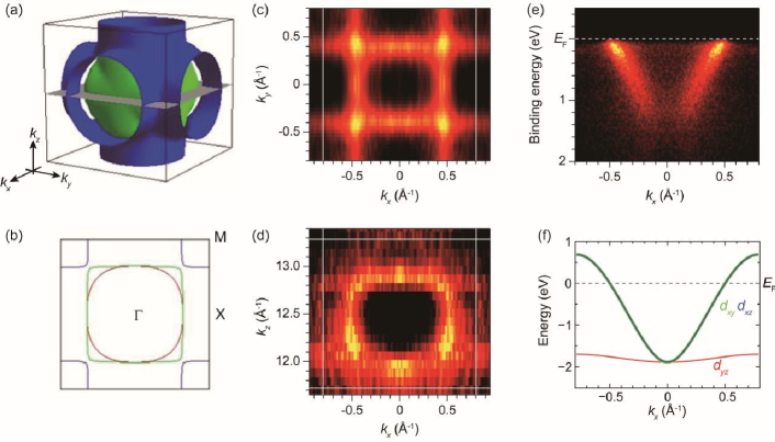
In order to investigate the electronic structure of the SrMoO3 film, we performed ARPES measurements in the two-dimensional k space. Here one can ignore the contribution of Mo6+ in the surface to the obtained data near , owning to its insulating state. The Fermi surface (FS) mapping on the - plane and the - plane (Figs. 4(c) and (d)), recorded with varying from 500 to 700 eV, exhibits strong intensity with parallel-cross and ellipse patterns. These results can be reproduced computationally (see FS in Figs. 4(a) and (b)), and assure the high quality of the film (apart from Mo6+ in the surface). It is remarkable that in Fig. 4(e), a parabolic-like dispersion is clearly seen from ARPES spectra near along the –– path (the cut in Fig. 4(c) for the direction with ). In the present experimental geometry, where -polarized incident light and the analyzer slit are in the mirror plane of the sample, the band having even parity with respect to the mirror plane is observable, while the the and bands having odd parity are not Yukawa et al. (2013). These considerations led us to conclude that the observed dispersion originates from the -derived band, which is again supported by the band structures (Fig. 4(f)).
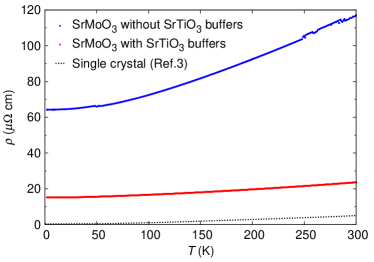
Figure 5 displays the temperature dependence of electrical resistivity of SrMoO3 films of thickness of about 16 nm on the KTaO3 substrate with and without the SrTiO3 buffer layer. Both films exhibit metallic temperature dependence but of the film with the buffer layer is notably smaller. When the buffer layer is employed, the RT resistivity drops to 24 cm (from 117 cm without the buffer layer). This value is smaller than the reported values of films with similar thickness, 34 cm Radetinac et al. (2016), but is five times larger than 5 cm for the bulk single crystal Nagai et al. (2005). Here, the contribution from the STO buffer to the resistivity is negligible, since the stoichiometric sample of SrTiO3 is a band insulator. It is also known that oxygen deficient samples SrTiO3-δ show metallic conduction, but is in the order of m cm for lightly and heavily -doped (oxygen deficient) samples Lin et al. (2014); Gong et al. (1991), which is times larger than that of SrMoO3 Nagai et al. (2005); Radetinac et al. (2016). The residual resistivity ratio RRR (=) of the film with and without the buffer layer shows almost the same value of 1.7–1.8, implying that the crystallinity of both films is similar. It is thus considered that the larger electrical resistivity of the film without the buffer layer arises from extrinsic effect such as grain boundaries and surface/interface impurities, as suggested from the RHEED and XRD observations (Figs. 1 and 2). Further efforts are necessary to improve the transport properties of SrMoO3 films, in conjunction with the clarification of the role of the presence and absence of the buffer layer for the amount of impurities with the Mo6+ state.
IV Conclusion
We have succeeded in growing SrMoO3 films using MBE growth technique. Introduction of SrTiO3 buffer layer of 4–8 unit cells between the SrMoO3 film and the (001)-oriented SrTiO3 or KTaO3 substrate improves the quality of the film, showing the five-times smaller resistivity than that of the film without the buffer layer. Clear observation of FS in ARPES measurements also ensures the high quality of the SrMoO3 film grown by MBE.
Acknowledgements
This work was supported by CREST (JPMJCR1421) and JSPS KAKENHI Grants (No. 16H06439 and No. 17H04849).
References
- Tilley (2016) R. J. D. Tilley, Perovskites: Structure-Property Relationships (John Wiley & Sons, Ltd., USA, 2016).
- Brixner (1960) L. H. Brixner, J. Inorg. Nucl. Chem. 14, 225 (1960).
- Nagai et al. (2005) I. Nagai, N. Shirakawa, S. Ikeda, R. Iwasaki, H. Nishimura, and M. Kosaka, Applied Physics Letters 87, 024105 (2005).
- Mackenzie (2017) A. P. Mackenzie, Rep. Prog. Phys. 80, 032501 (2017).
- Inukai and Murakami (1985) T. Inukai and T. Murakami, J. J. Appl. Phys. 24, 21 (1985).
- Mizoguchi et al. (2000) H. Mizoguchi, N. Kitamura, K. Fukumi, T. Mihara, J. Nishii, M. Nakamura, N. Kikuchi, H. Hosono, and H. Kawazoe, J. Appl. Phys. 87, 4617 (2000).
- Wanga et al. (2001) H. H. Wanga, D. F. Cuia, Y. L. Zhoua, Z. H. Chena, F. Chena, T. Zhaoa, H. B. L. G. Z. Yanga, M. C. Xub, Y. C. Lanb, X. L. Chenb, H. J. Qianc, and F. Q. Liuc, J. Cryst. Growth 226, 261 (2001).
- Radetinac et al. (2010) A. Radetinac, K. S. Takahashi, L. Alff, M. Kawasaki, and Y. Tokura, Appl. Phys. Express 3, 073003 (2010).
- Radetinac et al. (2014) A. Radetinac, A. Mani, S. Melnyk, M. Nikfalazar, J. Ziegler, Y. Zheng, R. Jakoby, L. Alff, and P. Komissinskiy, Appl. Phys. Lett. 105, 114108 (2014).
- Salg et al. (2019) P. Salg, D. Walk, L. Zeinar, A. Radetinac, L. Molina-Luna, A. Zintler, R. Jakoby, H. Maune, P. Komissinskiy, and L. Alff, APL Mater. 7, 051107 (2019).
- Radetinac et al. (2016) A. Radetinac, J. Zimmermann, K. Hoyer, H. Zhang, P. Komissinskiy, and L. Alffa, J. Appl. Phys. 119, 055302 (2016).
- Wadati et al. (2014) H. Wadati, J. Mravlje, K. Yoshimatsu, H. Kumigashira, M. Oshima, T. Sugiyama, E. Ikenaga, A. Fujimori, A. Georges, A. Radetinac, K. S. Takahashi, M. Kawasaki, , and Y. Tokura, Phys. Rev. B 90, 205131 (2014).
- Schlom (2015) D. G. Schlom, APL Mater. 3, 062403 (2015).
- Oka and Fukumura (2017) D. Oka and T. Fukumura, CrystEngComm 19, 2144 (2017).
- Wang et al. (2001) H. H. Wang, G. Z. Yang, D. F. Cui, H. B. Lu, T. Zhao, F. Chen, Y. L. Zhou, and Z. H. Chen, J. Vac. Sci. Tech. A 19, 930 (2001).
- not (a) (a), it has been reported that the value of the RT resistivity decreases from 34 cm to 27 cm with increasing the film thickness from 15 nm to 60 nm Radetinac et al. (2016). This result implies the influence of the oxidized surface of SrMoO3 films. Compared with samples with the same thickness, of our films in this study is 30% smaller than that of previous reports.
- Giannozzi et al. (2009) P. Giannozzi, S. Baroni, N. Bonini, M. Calandra, R. Car, C. Cavazzoni, D. Ceresoli, G. L. Chiarotti, M. Cococcioni, and I. Dabo, Journal of Physics: Condensed Matter 21, 395502 (2009).
- Giannozzi et al. (2017) P. Giannozzi, O. Andreussi, T. Brumme, O. Bunau, M. B. Nardelli, M. Calandra, R. Car, C. Cavazzoni, D. Ceresoli, and M. Cococcioni, Journal of Physics: Condensed Matter 29, 465901 (2017).
- Kresse and Joubert (1999) G. Kresse and D. Joubert, Phys. Rev. B 59, 1758 (1999).
- Perdew et al. (1996) J. P. Perdew, K. Burke, and M. Ernzerhof, Phys. Rev. Lett. 77, 3865 (1996).
- Macquart et al. (2010) R. B. Macquart, B. J. Kennedy, and M. Avdeev, J Solid State Chem. 183, 249 (2010).
- Kozuka et al. (2012) Y. Kozuka, H. Seki, T. C. Fujita, S. Chakraverty, K. Yoshimatsu, H. Kumigashira, M. Oshima, M. S. Bahramy, R. Arita, and M. Kawasaki, Chem. Mater. 24, 3746 (2012).
- Terashima et al. (1990) T. Terashima, Y. Bando, K. Iijima, K. Yamamoto, K. Hirata, K. Hayashi, K. Kamigaki, and H. Terauchi, Phys. Rev. Lett. 65, 2684 (1990).
- (24) S. Hasegawa, “Reflection high-energy electron diffraction”, Characterization of Materials, ed., E. N. Kaufmann (Wiley, New York, 2012). p. 1925 – 1938.
- Freund and Suresh (2003) L. B. Freund and S. Suresh, Thin Film Materials: Stress, Defect Formation and Surface Evolution (Cambridge University Press, Cambridge, 2003).
- Schubert et al. (2003) J. Schubert, O. Trithaveesak, A. Petraru, C. L. Jia, R. Uecker, P. Reiche, and D. G. Schlom, Appl. Phys. Lett. 82, 3460 (2003).
- Aschauer et al. (2013) U. Aschauer, R. Pfenninger, S. M. Selbach, T. Grande, and N. A. Spaldin, Phys. Rev. B 88, 054111 (2013).
- Colton et al. (1978) R. J. Colton, A. M. Guzman, and J. W. Rabalais, J. Appl. Phys. 49, 409 (1978).
- Scanlon et al. (2010) D. O. Scanlon, G. W. Watson, D. J. Payne, G. R. Atkinson, R. G. Egdell, and D. S. L. Law, J. Phys. Chem. C 114, 4636 (2010).
- not (b) (b), using the QUASES-IMFP-TPP2M software Tanuma et al. (1994), the inelastic mean free path (IMFP) of photoelectron from O 1s is about 2 nm in SrMoO3 for eV. With these IMFP and values, we roughly estimated 20% (80%) contributions from SrTiO3 (SrMoO3) to the O 1s spectrum. We also obtained 15–18% contributions from SrTiO3 to the Sr 3d spectrum, using the estimated IMFP of 2.3–2.5 nm and eV.
- Wagner et al. (1979) C. D. Wagner, W. M. Riggs, L. E. Davis, and J. F. M. G. E. Muilenberg, Handbook of x-ray photoelectron spectroscopy : a reference book of standard data for use in x-ray photoelectron spectroscopy (Perkin-Elmer Co., USA, 1979).
- Yukawa et al. (2013) R. Yukawa, S. Yamamoto, K. Ozawa, M. D’Angelo, M. Ogawa, M. G. Silly, F. Sirotti, and I. Matsuda, Phys. Rev. B 87, 115314 (2013).
- Lin et al. (2014) X. Lin, G. Bridoux, A. Gourgout, G. Seyfarth, S. Kramer, M. Nardone, B. Fauque, and K. Behnia, Phys. Rev. Lett. 112, 207002 (2014).
- Gong et al. (1991) W. Gong, H. Yun, Y. B. Ning, J. E. Greedan, W. R. Datars, and C. V. Stager, J. Solid State Chem. 90, 320 (1991).
- Tanuma et al. (1994) S. Tanuma, C. J. Powell, and D. R. Penn, Surf. Interf. Anal. 21, 165 (1994).