Quantum photonics in triangular-cross-section nanodevices in silicon carbide
Abstract
Silicon carbide is evolving as a prominent solid-state platform for the realization of quantum information processing hardware. Angle-etched nanodevices are emerging as a solution to photonic integration in bulk substrates where color centers are best defined. We model triangular cross-section waveguides and photonic crystal cavities using Finite-Difference Time-Domain and Finite-Difference Eigensolver approaches. We analyze optimal color center positioning within the modes of these devices and provide estimates on achievable Purcell enhancement in nanocavities with applications in quantum communications. Using open quantum system modeling, we explore emitter-cavity interactions of multiple non-identical color centers coupled to both a single cavity and a photonic crystal molecule in SiC. We observe polariton and subradiant state formation in the cavity-protected regime of cavity quantum electrodynamics applicable in quantum simulation.
1 Introduction
Color center photonics has been on the rise in explorations of quantum information processing. Initially, the negatively charged nitrogen vacancy in diamond was explored as a solid-state qubit that can be individually initialized, manipulated and measured with high fidelity even at room temperature [1, 2]. Owing to the lack of availability of wafer-scale substrates and color center emission at telecommunications wavelengths, new material hosts have been explored as potential defect hosts. Among them, silicon carbide (SiC) gained attention as a substrate whose color centers have long spin coherence times [3, 4, 5], excellent brightness [6] and manipulations of nuclear spin [7, 8], and are suitable for applications in quantum computing [9, 10, 8], quantum photonics [11, 12], quantum communications [13, 6, 14, 15], quantum sensing [16, 17, 18, 19, 20], quantum metrology [21, 22] and quantum simulation [23, 24, 25, 26, 27]. In addition, SiC has benefits like large bandgap, high thermal conductivity, strong second-order non-linearity, infra-red emitting color centers, and has a decades-long industrial presence.
It has been well studied in atomic [28] and quantum dot [29, 30] systems that optical resonators enhance emitter properties, from Purcell emission enhancement and coupling to a desired mode to polariton physics and cavity Quantum Electrodynamics (cQED). These effects have been used in high-speed quantum light generation, all-optical switching, creation of hybridized light-matter states, and more. The advantages of integrated photonics with color centers lie in scalability granted by the combination of the solid-state platform and the nearly identical optical properties of ensembles [31], inaccessible to the previously studied systems.
A key requirement for nanophotonic integration is the ability to grow or place high quality, high refractive index thin films on a contrasting substrate which can facilitate high optical confinement in nanostructures. For example, the ability to bond silicon on insulator in a scalable way launched silicon as a strong material platform for photonics applications [32]. Although commercial scale high quality crystalline SiC wafers grown using homoepitaxy (MBE, CVD) or sublimation have transferred into color center research, for example by in situ doping of vanadium centers in 4H-SiC [33], this approach does not provide an undercutting layer needed to generate freestanding photonic devices. On the other hand, growth of 3C-SiC on silicon has been established in MEMS research [34], but has not lent itself well for color center formation in nanoscale films due to the lattice mismatch damage [35]. These substrate limitations have been circumvented via photo-electrochemical etching [36] and SiC thinning and bonding to an insulator [37]. While these approaches successfully integrated and manipulated color centers in a nanocavity, the fabrication processes have been limited in terms of either type or size of the substrate, requiring a specific doping profile or a limited chip area.
Another bulk substrate nanofabrication approach, initially championed in diamond [38], has been emerging in silicon carbide: the angle-etching method [39]. In contrast to the more traditional (rectangular) profile, the photonic devices created via angle-etch have a triangular cross-section. Such SiC processing methods are currently based on the Faraday-cage assisted etching; still, wafer scale processes could be implemented using ion beam etching [40]. Triangular device geometry resolves the problem of the unavailability of heteroepitaxial thin film color center substrates because it can be implemented in bulk substrates of any polytype or doping level. However, due to the novelty of the approach, not much is known about the optical properties and parameters related to the color center integration into angle-etched SiC devices.
This paper studies triangularly shaped nanophotonic devices in SiC suitable for the development of quantum communication and quantum simulation hardware. Nitrogen vacancy and vanadium impurity in 4H-SiC are of particular interest in this work, since their emission wavelengths are in the telecommunications range which makes them useful candidates for long-distance quantum information distribution. Using Lumerical MODE and FDTD software packages, we examine the TE and TM polarized modes in the near infrared (NIR) part of the spectrum supported in triangular waveguides with variable etch-angles, characterizing their effective index of refraction and the depth of the mode maximum. We design high / ratio photonic crystal cavities and analyze their resonance parameters and potential Purcell enhancement for variable triangular profiles. We extend this design into a photonic crystal molecule with coupled cavity array integration in sight. Finally, using open quantum system modeling, we explore emitter-cavity interactions of multiple non-identical color centers coupled to both a single cavity and a photonic crystal molecule, observing polariton and subradiant states formation.
2 SiC color center emission properties
While all SiC polytypes can host color centers in highly crystalline form, their processing into a photonic platform can induce irreversible lattice damage that prevents formation of well-defined quantum emitters. Advanced 4H-SiC carbide processing techniques have made this polytype a promising candidate for color-center integrated nanophotonics. 4H-SiC has a hexagonal close-packed lattice with two inequivalent lattice sites: the hexagonal site, , and the quasi-cubic site, ; this inequivalency allows for 4 defect orientations (, , , and ) in a two-site defect, with each defect orientation contributing its own zero-phonon line (ZPL) to the spectrum. The most prominently studied centers in 4H-SiC polytype are shown in Table 1. As solid-state emitters, color centers interact with the host lattice which modifies their optical properties. The proportion of radiative emission occurring through the zero-phonon transition compared to the transitions to all vibronic levels is given by the Debye-Waller (DW) factor . Integration into high quality factor () and small mode volume () cavities can rebalance this ratio via the Purcell effect. The radiative emission enhancement is given by the Purcell factor:
The terms and refer to the cavity-color center spatial overlap and spectral matching respectively. A photonic crystal cavity (PCC) enabling large Purcell enhancement ensures a high emission rate of indistinguishable photons needed for the implementation of quantum entanglement schemes [41].
| Defect | ZPL wavelength | DW factor | Emission | Calculated | Purcell |
|---|---|---|---|---|---|
| (nm) | lifetime | (GHz) | enhancement | ||
| V1’ (V) [42] | 858 | 19% | (5.6 1.2) ns | 3.41 | 120 10 [37] |
| V1 (V) [43] | 861 | 8% | (5.5 1.4) ns | 2.23 | 25 [36] |
| V2 (V) [43, 44] | 918 | 9% | 6 ns | 2.27 | - |
| Cr4+ [45] | 1070 | 75% | 145.8 9.7 s | 0.04 | - |
| VV0 () [46, 20] | 1130 | (5.3 1.1)% | (14 3) ns | 1.14 | 53[47] |
| VNC [48] | 1176 - 1243 | - | 2.2 ns | - | |
| V4+ () [49] | 1279 | 25% | 167 ns | 0.72 | - |
| V4+ () [49] | 1335 | 50% | 41 ns | 2.04 |
3 Triangular cross-section SiC waveguide
A waveguide uses total internal reflection to confine propagating light in the high refractive index material. The triangular cross-section waveguide modeled in this study using Finite-Difference Eigensolver (Lumerical MODE) was parametrized by the wavelength to the top-width ratio / and the half-angle . The fundamental TE and TM modes were studied for and with obtained mode profiles shown in Figure 1.
To find the optimal positioning of the color center in the waveguide, we analyzed the depth at which the electric field intensity maximum () of a mode is positioned relative to the waveguide’s top plane. As / increases, for the fundamental TE (TM) polarized mode shifts towards (away from) the top waveguide surface i.e., the depth decreases (increases). This behavior is consistent for all studied half-angle values , as shown in Figure 2a. For higher values of /, the mode becomes less confined and the evanescent losses into the surrounding medium dominate, as can be observed in mode profiles in Figure 1. These observations are consistent with the trend in the effective refractive index () values shown in Figure 2b. The effective refractive index for a mode is given by the ratio of propagation constant of that mode () to the wavenumber in vacuum (). When , significantly below the SiC refractive index , for the TM mode lies outside the waveguide and results in a lossy propagation. These results give an understanding into the range of half-angle and values suitable for fabricating triangular cross-section waveguides that are able to couple the fundamental TE/TM modes with other photonic elements.
4 Triangular cross-section SiC photonic crystal cavity
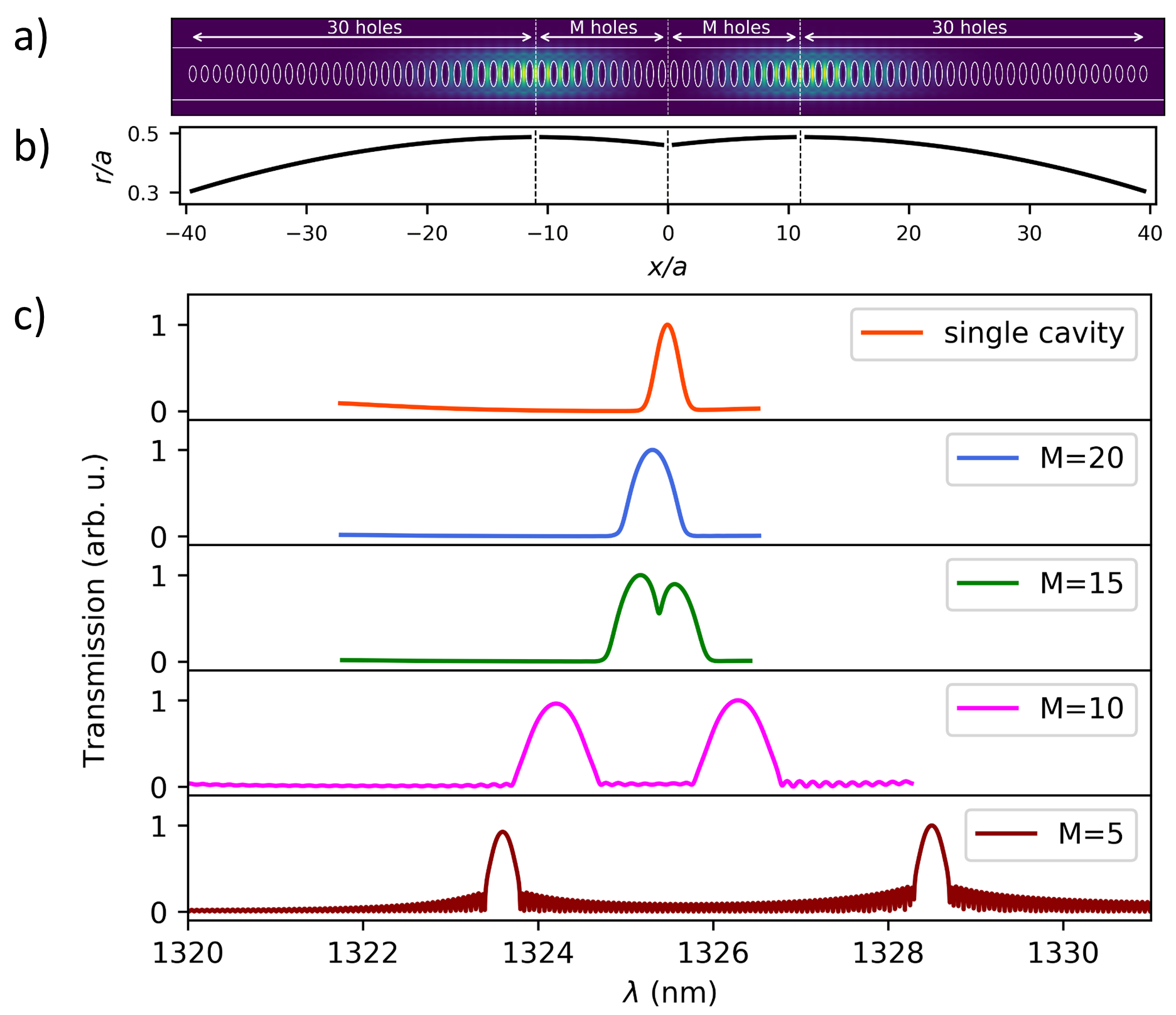
Photonic crystal cavities are nanostructures with periodic variation of refractive index which localize photons to sub-wavelength mode volumes. The triangular nanobeam photonic crystal cavities explored in this study have elliptical air holes whose major axis radius is tapered along the device, which have proved successful in diamond color center research in achieving ultra-high Q-factors and ultra-small mode volumes [50, 51] and more importantly, offer better mode confinement and scalability than the well-explored methods. As shown in Figure 3, the cavity has a width and consists of 30 through holes on either side of the center of the cavity with uniform spacing between the holes, lattice constant nm. The minor radius of the holes is and to minimize scattering and maximize Q-factor, the major radius is quadratically varied from to over 30 holes. The beam has a triangular cross-section with a half-angle = .
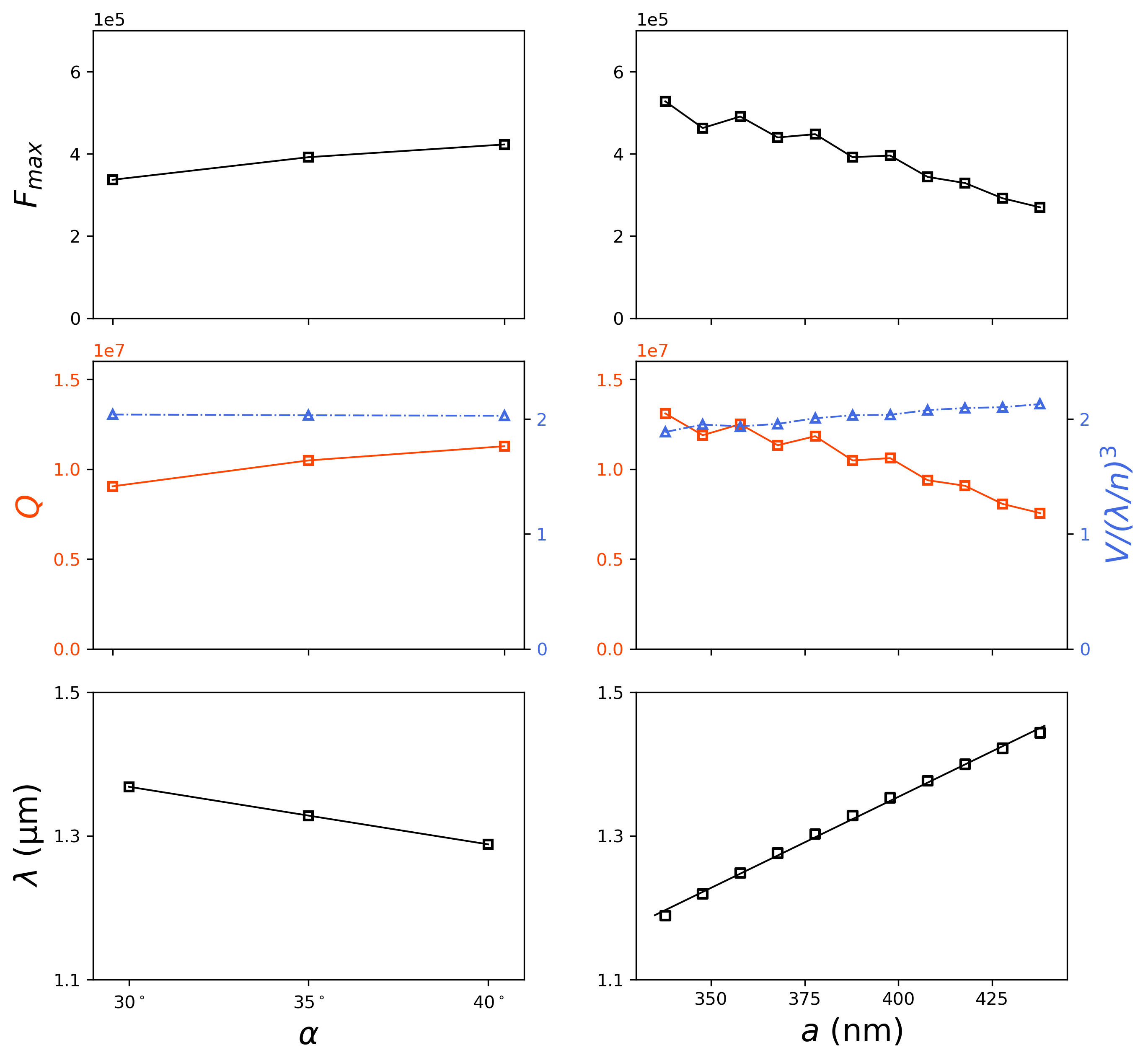
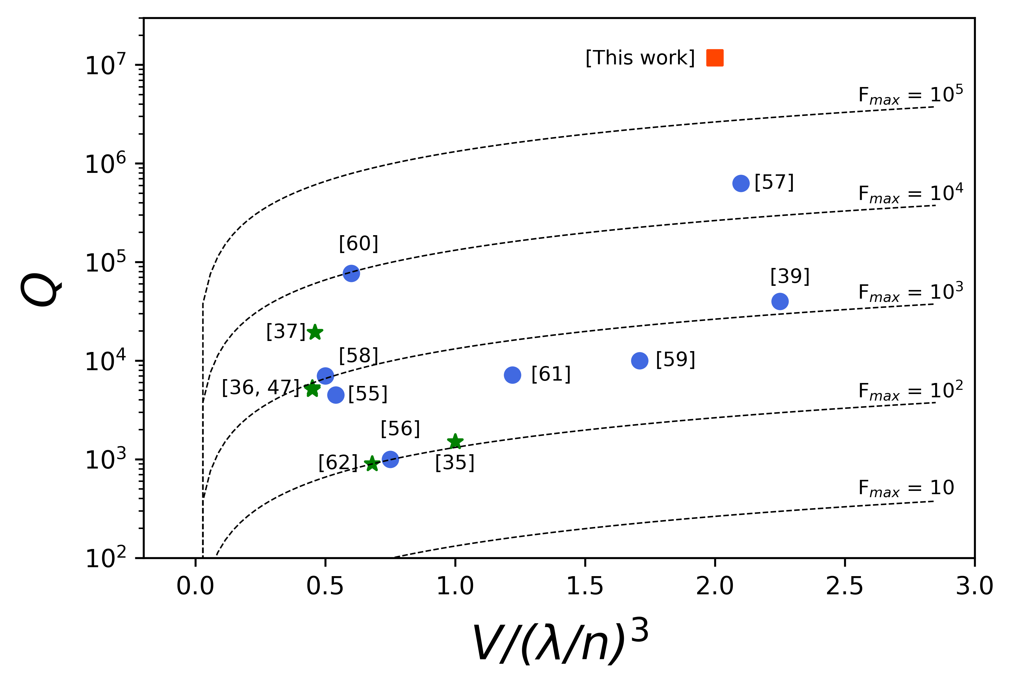
The optical response of the triangular nanobeams was modeled using the Finite-Difference Time-Domain method in the Lumerical FDTD software package. In the simulations, SiC was defined as a dielectric with a constant refractive index . The electric field profile of the fundamental mode is shown in Figure 4a. The fundamental cavity resonance occurs at nm with a quality factor of and mode volume of . Higher order TE-polarized longitudinal modes, useful for nonlinear optics processes involving multiple modes such as frequency conversion [52, 53, 37, 54], are also supported in the cavity, as shown in Figure 4b-d, where the cross-sectional profile is representative of the profiles of the electrical field nodes in all modes. Cavities with half-angle were simulated while maintaining the lattice constant and radii of the holes. It was observed that the resonant wavelength of the fundamental mode decreased with increasing , whereas the Q-factor and mode volume remained almost the same, as shown in Figure 5. The impact of a changing lattice constant was studied across a range of 100 nm, which tuned the resonant wavelength from 1200 nm to 1500 nm, as shown in Figure 5. The Q-factor and mode volume of the fundamental resonance for varying values of remained nearly constant (less than a factor of 2 for and within for ). Thus, for different technological implementations of the inclines in angled etching, this tapered-hole design of a photonic cavity can be used to integrate various SiC color centers in the telecommunications wavelength range with strong Purcell enhancement of in the range of - when the spatial and spectral overlap terms are unity. Figure 6 compares the simulated and values in this work to other photonic crystal cavities fabricated in SiC. The cavities without emitters achieved quality factors up to 630,000 [55, 56, 57, 58, 39, 59, 60, 61] and those with emitters achieved up to 19,300 with Purcell enhancement up to 120 [37, 35, 36, 47, 62], showing that our design bridges the gap between color center platforms and high Purcell enhancement devices.
Triangular photonic crystal geometry lends itself well toward the 1D coupled cavity array fabrication. To study the coupling between the neighboring cavities, a photonic crystal molecule was designed by stacking two photonic crystal cavities side-by-side with a reduced number of holes in the interior () as shown in Figure 7a. The major axis radius of the M holes is tapered using the same parabolic variation as the 30 holes with the M largest holes kept and 30-M holes discarded. The coupling between the two cavities causes the resonant mode splitting. We observe in the transmission spectra that as the separation between the two cavities is reduced ( decreases), the coupling strength between the cavities represented in the wavelength separation between the two resonances increases [63]. By integrating emitters into the photonic crystal molecule, the designed structures can be employed for investigation of cQED effects [64].
5 Multi-emitter cavity QED in SiC photonic devices
Strong coupling between light and matter lies at the crux of many applications of optics, including all-optical quantum gates for quantum computing [65, 66] and quantum simulations of strongly correlated condensed matter systems [67]. While cQED physics has been realized in single quantum dot systems [68, 69] and single defects in semiconductors [70], the integration of multiple quantum emitters into cavities has been suggested as a method of accessing the strong coupling regime for emitters with smaller cavity-emitter coupling terms [31]. In a multi-emitter system, the emitters that are coupled individually to the same cavity will effectively behave as a single emitter with emitter-cavity coupling enhanced by a factor of . In order to determine whether this strong coupling effect will occur in the triangular cavity devices described above, the quantum master equation was solved using QuTiP, an open source python package for simulating open quantum systems[71].
The Tavis-Cummings model describes such a multi-emitter system and is given by the Hamiltonian:
where and are the cavity frequency and the emitter frequencies, respectively, and represent the cavity annihilation operator and the -th emitter lowering operators. Parameters refer to the cavity-emitter coupling rates whose maximal value can be calculated by the equation:
and depends on the positioning of the emitter relative to the electric field profile of the cavity by the relationship . is the electric field intensity at the color center, and is the angle between the orientation of color center dipole and the electric field. As detailed above, the mode volume of the simulated triangular photonic crystal cavity is , and the values of the optical lifetime and the Debye-Waller factor are dependent upon the choice of the color center (see Table 1). The calculated values of in SiC are given in Table 1. The loss in the system is simulated via Lindblad dissipators using loss parameters for cavity and for each emitter [72].
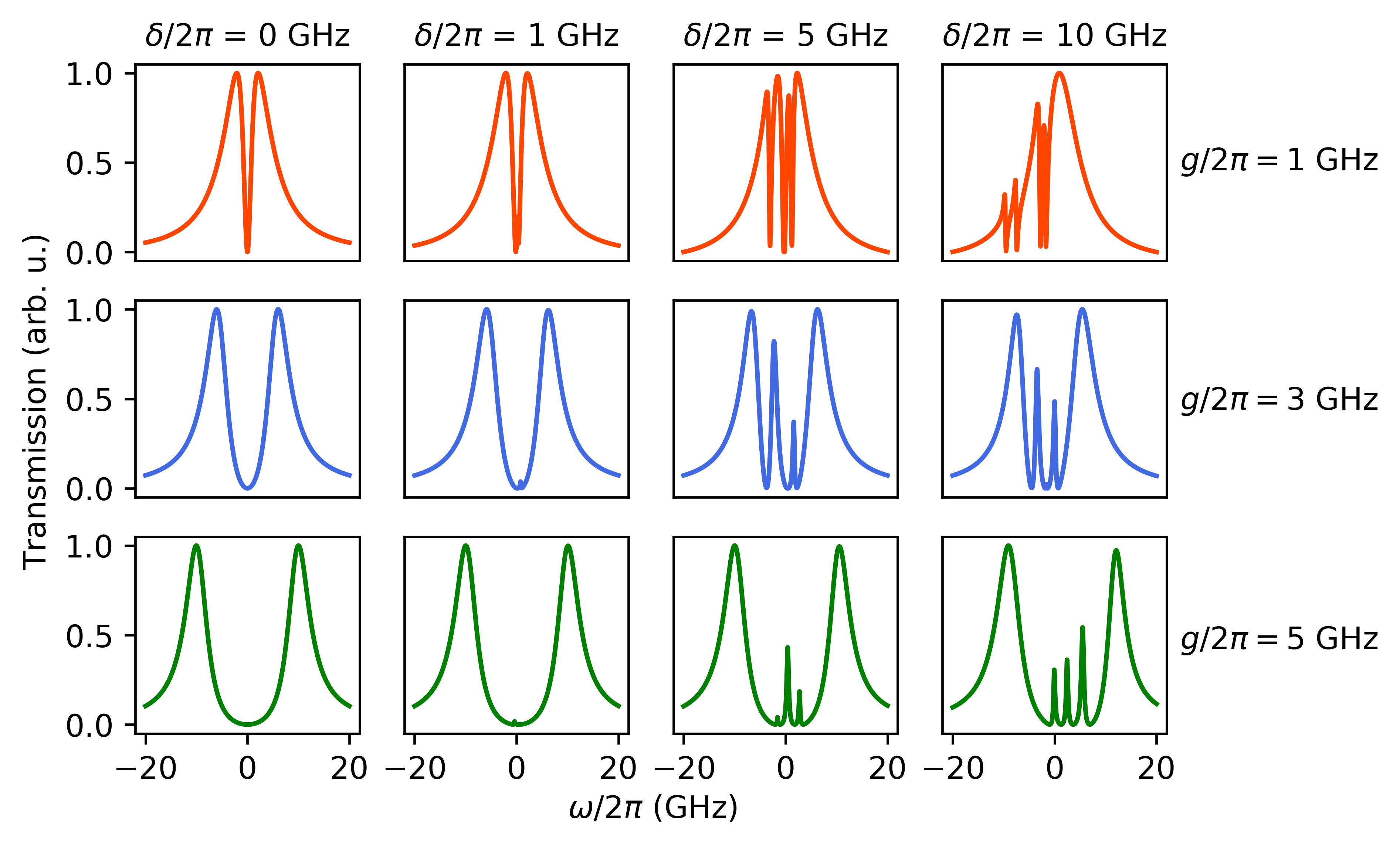
A suitable range of values was selected for simulations, and the resulting transmission spectra of a single cavity coupled to emitters are shown in Figure 8. The emission frequencies of the emitters are randomly generated from a Gaussian distribution centered at the cavity resonance with a standard deviation , where represents the inhomogeneous broadening in the color center ensemble. The splitting of the transmission spectrum into two separate polariton peaks separated by confirms that the system is in the strong cQED coupling regime for both values of 3 GHz and 5 GHz. Figure 8 shows that the expected cavity-emitter polariton peak splitting persists for values of . Furthermore, the linewidth of the split emitter-cavity polariton peaks is , which indicates these systems exist within the cavity-protection domain wherein the emitter ensemble is protected from inhomogeneous broadening caused by the dephasing [73].
Photonic quantum simulation proposals [74] rely on the use of coupled cavity arrays in the strong coupling regime of cQED. Here, we explore the smallest such system of coupled nanocavities, as modeled in Figure 9, and in relation to the designed photonic crystal molecule in Figure 7. In order to explore the physics of such a system, the Tavis-Cummings model can be expanded upon by adding a cavity coupling term to form the Tavis-Cummings-Hubbard (TCH) model:
where is the number of cavities, , and are the resonant frequency of, the number of emitters in, and the annihilation operator of the -th cavity. The resonant frequency of the -th emitter in the -th cavity is and it has the annihilation operator . The coupling rate between neighboring cavities is given by .
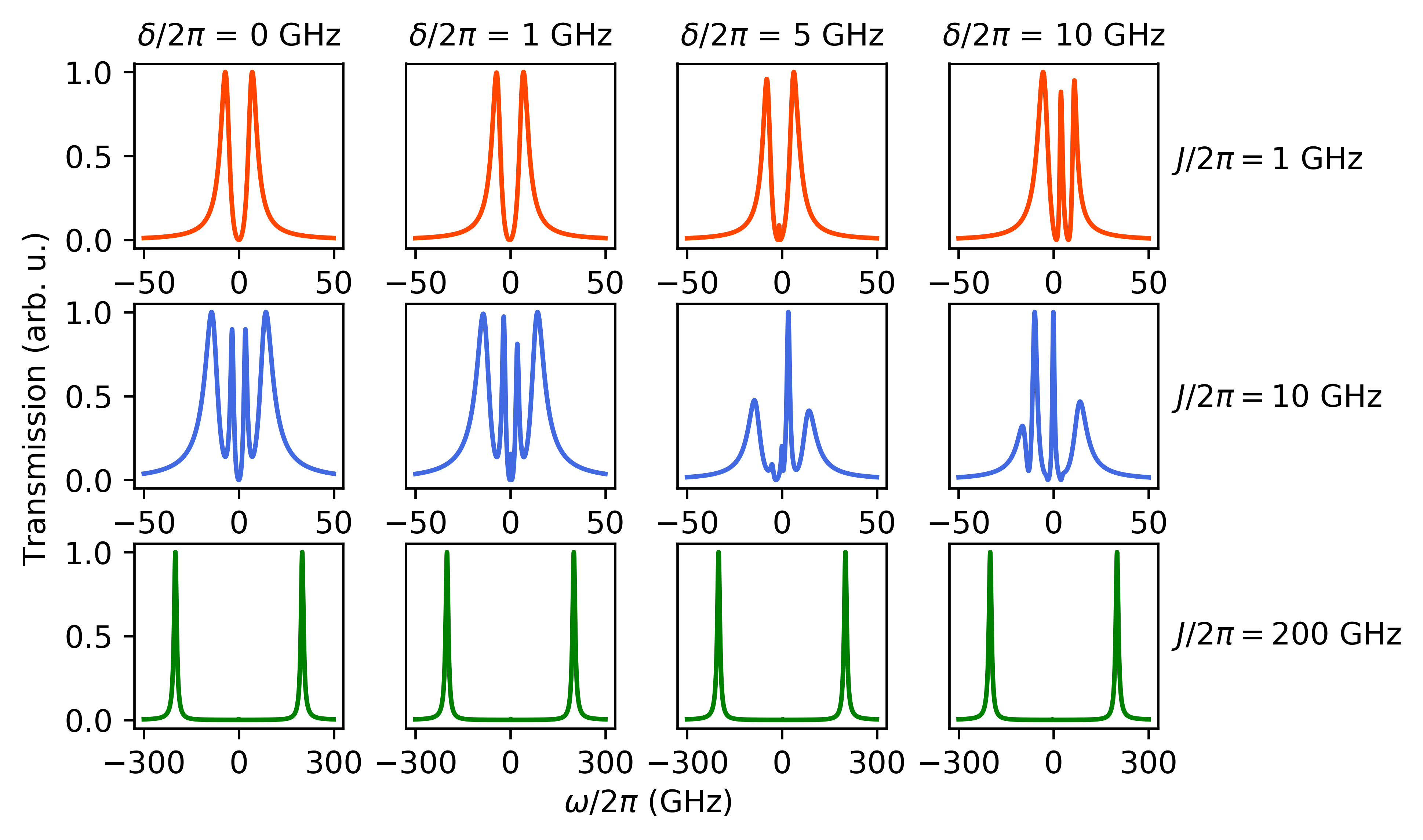
The transmission spectra of cavities with emitters coupled to each cavity for GHz were simulated in QuTiP with and without broadening in emitter frequencies and the results are shown in Figure 9. We extracted values of the photon hopping rate by fitting a two-peak Lorentzian to the plots in Figure 7; the splitting of polariton peaks in strongly coupled systems is directly proportional to the coupling strength. The GHz and GHz photonic crystal molecule cQED plots exhibit the same cavity protection linewidth signature and peak splitting as the single cavity simulations. The structure of the GHz set of simulations merits some closer discussion; the eigenvalues of the lossless TCH model when in a fully resonant case are and , as seen in the GHz, GHz plot in Figure 9. This same set of peaks is maintained for the values of , which means that light-matter hybridized states continue even with the introduction of modest, but realistic, inhomogeneous broadening into the system. These results demonstrate that the designed triangular cross-section devices are strong candidates for quantum information and simulation platforms. In addition, the inhomogeneously broadened emitter systems exhibit subradiant peaks, which have been studied in single-cavity systems and found to facilitate coherence conducive to high-purity quantum light generation [75].
6 Discussion
Our modeling results provide insights into color center integration with triangular SiC photonic devices, as well as quantum optical phenomena in cavity QED systems. This geometry is of great interest because it overcomes the limitations of color center platforms requiring implementation in bulk substrates.
Triangular-cross-section waveguides are found to efficiently guide the light emission from color centers embedded at optimal depths. The waveguides support propagation of both TE and TM polarized modes, thus serving a variety of color center crystalline orientations. Fabrication imperfections in the curvature of the apex affect only the modes present in the lower half of the triangular cross-section. Similar designs fabricated in diamond have successfully combined triangular waveguide geometry with suitable grating couplers for efficient collection of light into a high numerical aperture objective, as well as tapered down for coupling to an optical fiber [76]. They can also be designed for integration with the emerging superconducting nanowire single-photon detectors [77].
The modeled triangular nanobeam photonic crystal cavities have high / ratio with promising applications in high-speed and indistinguishable photon generation. For the same triangular geometry, altering of the lattice constant is found to tune the resonant wavelength without reduction in the quality factor, meaning that many different high-performing devices can be simultaneously fabricated on the same chip. Interestingly, in literature on diamond and SiC nanobeam devices, the fabricated quality factors fell 2-3 orders of magnitude short of their theoretical predictions [51, 39]. The reduced performance can be attributed to fabrication errors such as mask alignment imperfections [39]. This indicates that additional efforts in nanofabrication process development need to be invested to realize the full application potential of these designs. Purcell enhancement of the zero-phonon line emission would play a crucial role in realizing quantum systems that require two-photon interference and quantum entanglement, such as quantum repeaters [78] and cluster-entangled states [79, 80]. The photonic crystal cavities modeled in this work potentially provides a tie-in between high / designs and platforms that host color centers, a necessary step for color center-based quantum information technologies in SiC.
The open quantum system modeling of a single nanocavity and a photonic crystal molecule integrating non-identical color centers confirmed that cavity-protection effects can support polariton physics even in the presence of realistic inhomogeneous broadening in SiC structures. Extensions to larger 1D coupled-cavity-arrays can provide a simulation testbed for proposals of strongly-correlated systems, such as the 1D Mott insulator to superfluid transition [81], and could be extended to waveguide QED simulations of the many-body localization phase [82].
Our simulations of triangular cross-section waveguides and cavities in 4H-SiC demonstrate that this geometry can achieve similar figures of merit (e.g. Q ) as other state-of-the-art geometries in both 4H- and 3C-SiC polytype. Since, the thickness and width of these devices are related through the etch angle, global scaling is possible without affecting the figures of merit as much. The benefit to our approach is that 4H-SiC can host color centers without damaging the lattice unlike 3C-SiC and the geometry is highly scalable using angle RIE etching unlike some of the more complex 2D photonic crystal cavities. In fact, triangular cross-section nanophotonics have already been successfully fabricated in diamond; the work already performed in diamond has illuminated some shortfalls in nanofabrication that need to be overcome before we can fully realize our simulated results. The prior experiments and our work in this paper pave the way toward high quality, color center integrated, highly scalable nanophotonic devices in 4H-SiC.
7 Acknowledgments
This work is supported by the National Science Foundation (CAREER-2047564) and the UC Davis Summer GSR Award for Engineering or Computer-related Applications and Methods. The authors thank Richard Scalettar and Jesse Patton for fruitful discussions on Tavis-Cummings-Hubbard physics.
References
- [1] P Neumann, N Mizuochi, F Rempp, Philip Hemmer, H Watanabe, S Yamasaki, V Jacques, Torsten Gaebel, F Jelezko, and J Wrachtrup. Multipartite entanglement among single spins in diamond. Science, 320(5881):1326–1329, 2008.
- [2] Victoria A. Norman, Sridhar Majety, Zhipan Wang, William H. Casey, Nicholas Curro, and Marina Radulaski. Novel color center platforms enabling fundamental scientific discovery. InfoMat, 2020.
- [3] Matthias Widmann, Sang-Yun Lee, Torsten Rendler, Nguyen Tien Son, Helmut Fedder, Seoyoung Paik, Li-Ping Yang, Nan Zhao, Sen Yang, Ian Booker, et al. Coherent control of single spins in silicon carbide at room temperature. Nature Materials, 14(2):164–168, 2015.
- [4] David J Christle, Abram L Falk, Paolo Andrich, Paul V Klimov, Jawad Ul Hassan, Nguyen T Son, Erik Janzén, Takeshi Ohshima, and David D Awschalom. Isolated electron spins in silicon carbide with millisecond coherence times. Nature Materials, 14(2):160–163, 2015.
- [5] Hosung Seo, Abram L Falk, Paul V Klimov, Kevin C Miao, Giulia Galli, and David D Awschalom. Quantum decoherence dynamics of divacancy spins in silicon carbide. Nature Communications, 7(1):1–9, 2016.
- [6] Stefania Castelletto, BC Johnson, Viktor Ivády, N Stavrias, T Umeda, A Gali, and T Ohshima. A silicon carbide room-temperature single-photon source. Nature Materials, 13(2):151–156, 2014.
- [7] Abram L Falk, Paul V Klimov, Viktor Ivády, Krisztián Szász, David J Christle, William F Koehl, Ádám Gali, and David D Awschalom. Optical polarization of nuclear spins in silicon carbide. Physical Review Letters, 114(24):247603, 2015.
- [8] Paul V Klimov, Abram L Falk, David J Christle, Viatcheslav V Dobrovitski, and David D Awschalom. Quantum entanglement at ambient conditions in a macroscopic solid-state spin ensemble. Science Advances, 1(10):e1501015, 2015.
- [9] Pieter Kok, William J Munro, Kae Nemoto, Timothy C Ralph, Jonathan P Dowling, and Gerard J Milburn. Linear optical quantum computing with photonic qubits. Reviews of Modern Physics, 79(1):135, 2007.
- [10] JR Weber, WF Koehl, JB Varley, A Janotti, BB Buckley, CG Van de Walle, and David D Awschalom. Quantum computing with defects. Proceedings of the National Academy of Sciences, 107(19):8513–8518, 2010.
- [11] Mete Atatüre, Dirk Englund, Nick Vamivakas, Sang-Yun Lee, and Joerg Wrachtrup. Material platforms for spin-based photonic quantum technologies. Nature Reviews Materials, 3(5):38–51, 2018.
- [12] William F Koehl, Bob B Buckley, F Joseph Heremans, Greg Calusine, and David D Awschalom. Room temperature coherent control of defect spin qubits in silicon carbide. Nature, 479(7371):84–87, 2011.
- [13] Bas Hensen, Hannes Bernien, Anaïs E Dréau, Andreas Reiserer, Norbert Kalb, Machiel S Blok, Just Ruitenberg, Raymond FL Vermeulen, Raymond N Schouten, Carlos Abellán, et al. Loophole-free Bell inequality violation using electron spins separated by 1.3 kilometres. Nature, 526(7575):682–686, 2015.
- [14] Junfeng Wang, Yu Zhou, Ziyu Wang, Abdullah Rasmita, Jianqun Yang, Xingji Li, Hans Jürgen von Bardeleben, and Weibo Gao. Bright room temperature single photon source at telecom range in cubic silicon carbide. Nature Communications, 9(1):1–6, 2018.
- [15] Abram L Falk, Bob B Buckley, Greg Calusine, William F Koehl, Viatcheslav V Dobrovitski, Alberto Politi, Christian A Zorman, Philip X-L Feng, and David D Awschalom. Polytype control of spin qubits in silicon carbide. Nature Communications, 4(1):1–7, 2013.
- [16] HJ Mamin, M Kim, MH Sherwood, CT Rettner, K Ohno, DD Awschalom, and D Rugar. Nanoscale nuclear magnetic resonance with a nitrogen-vacancy spin sensor. Science, 339(6119):557–560, 2013.
- [17] Georg Kucsko, Peter C Maurer, Norman Ying Yao, Michael Kubo, Hyun Jong Noh, Po Kam Lo, Hongkun Park, and Mikhail D Lukin. Nanometre-scale thermometry in a living cell. Nature, 500(7460):54–58, 2013.
- [18] Christian L Degen, F Reinhard, and Paola Cappellaro. Quantum sensing. Reviews of Modern Physics, 89(3):035002, 2017.
- [19] D Simin, VA Soltamov, AV Poshakinskiy, AN Anisimov, RA Babunts, DO Tolmachev, EN Mokhov, M Trupke, SA Tarasenko, A Sperlich, et al. All-optical dc nanotesla magnetometry using silicon vacancy fine structure in isotopically purified silicon carbide. Physical Review X, 6(3):031014, 2016.
- [20] Abram L Falk, Paul V Klimov, Bob B Buckley, Viktor Ivády, Igor A Abrikosov, Greg Calusine, William F Koehl, Ádám Gali, and David D Awschalom. Electrically and mechanically tunable electron spins in silicon carbide color centers. Physical Review Letters, 112(18):187601, 2014.
- [21] Vittorio Giovannetti, Seth Lloyd, and Lorenzo Maccone. Advances in quantum metrology. Nature Photonics, 5(4):222, 2011.
- [22] G Wolfowicz, SJ Whiteley, and DD Awschalom. Electrometry by optical charge conversion of deep defects in 4H-SiC. Proceedings of the National Academy of Sciences, 115(31):7879–7883, 2018.
- [23] Jianming Cai, Alex Retzker, Fedor Jelezko, and Martin B Plenio. A large-scale quantum simulator on a diamond surface at room temperature. Nature Physics, 9(3):168–173, 2013.
- [24] Ya Wang, Florian Dolde, Jacob Biamonte, Ryan Babbush, Ville Bergholm, Sen Yang, Ingmar Jakobi, Philipp Neumann, Alán Aspuru-Guzik, James D Whitfield, et al. Quantum simulation of helium hydride cation in a solid-state spin register. ACS Nano, 9(8):7769–7774, 2015.
- [25] Alán Aspuru-Guzik and Philip Walther. Photonic quantum simulators. Nature Physics, 8(4):285–291, 2012.
- [26] Iulia M Georgescu, Sahel Ashhab, and Franco Nori. Quantum simulation. Reviews of Modern Physics, 86(1):153, 2014.
- [27] Nicholas C. Harris, Gregory R. Steinbrecher, Mihika Prabhu, Yoav Lahini, Jacob Mower, Darius Bunandar, Changchen Chen, Franco N. C. Wong, Tom Baehr-Jones, Michael Hochberg, Seth Lloyd, and Dirk Englund. Quantum transport simulations in a programmable nanophotonic processor. Nature Photonics, 11(7):447–452, 2017.
- [28] H Jeff Kimble. Strong interactions of single atoms and photons in cavity qed. Physica Scripta, 1998(T76):127, 1998.
- [29] J Pelal Reithmaier, G Sęk, A Löffler, C Hofmann, S Kuhn, S Reitzenstein, LV Keldysh, VD Kulakovskii, TL Reinecke, and A Forchel. Strong coupling in a single quantum dot–semiconductor microcavity system. Nature, 432(7014):197–200, 2004.
- [30] Sonia Buckley, Kelley Rivoire, and Jelena Vučković. Engineered quantum dot single-photon sources. Reports on Progress in Physics, 75(12):126503, 2012.
- [31] Marina Radulaski, Kevin A Fischer, and Jelena Vučković. Nonclassical light generation from III–V and group-IV solid-state cavity quantum systems. In Advances In Atomic, Molecular, and Optical Physics, volume 66, pages 111–179. Elsevier, 2017.
- [32] Winnie N Ye and Yule Xiong. Review of silicon photonics: history and recent advances. Journal of Modern Optics, 60(16):1299–1320, 2013.
- [33] Robin Karhu, Einar Ö Sveinbjörnsson, Björn Magnusson, Ivan G Ivanov, Örjan Danielsson, and Jawad Ul Hassan. CVD growth and properties of on-axis vanadium doped semi-insulating 4H-SiC epilayers. Journal of Applied Physics, 125(4):045702, 2019.
- [34] Gabriel Ferro. 3C-SiC heteroepitaxial growth on silicon: the quest for holy grail. Critical Reviews in Solid State and Materials Sciences, 40(1):56–76, 2015.
- [35] Greg Calusine, Alberto Politi, and David D Awschalom. Silicon carbide photonic crystal cavities with integrated color centers. Applied Physics Letters, 105(1):011123, 2014.
- [36] David O Bracher, Xingyu Zhang, and Evelyn L Hu. Selective Purcell enhancement of two closely linked zero-phonon transitions of a silicon carbide color center. Proceedings of the National Academy of Sciences, 114(16):4060–4065, 2017.
- [37] Daniil M Lukin, Constantin Dory, Melissa A Guidry, Ki Youl Yang, Sattwik Deb Mishra, Rahul Trivedi, Marina Radulaski, Shuo Sun, Dries Vercruysse, Geun Ho Ahn, et al. 4H-silicon-carbide-on-insulator for integrated quantum and nonlinear photonics. Nature Photonics, 14(5):330–334, 2020.
- [38] Michael J Burek, Nathalie P De Leon, Brendan J Shields, Birgit JM Hausmann, Yiwen Chu, Qimin Quan, Alexander S Zibrov, Hongkun Park, Mikhail D Lukin, and Marko Lončar. Free-standing mechanical and photonic nanostructures in single-crystal diamond. Nano Letters, 12(12):6084–6089, 2012.
- [39] Bong-Shik Song, Seungwoo Jeon, Heungjoon Kim, Dongyeon Daniel Kang, Takashi Asano, and Susumu Noda. High-Q-factor nanobeam photonic crystal cavities in bulk silicon carbide. Applied Physics Letters, 113(23):231106, 2018.
- [40] Haig A Atikian, Pawel Latawiec, Michael J Burek, Young-Ik Sohn, Srujan Meesala, Normand Gravel, Ammar B Kouki, and Marko Lončar. Freestanding nanostructures via reactive ion beam angled etching. APL Photonics, 2(5):051301, 2017.
- [41] ÖO Soykal, Pratibha Dev, and Sophia E Economou. Silicon vacancy center in 4 h-sic: Electronic structure and spin-photon interfaces. Physical Review B, 93(8):081207, 2016.
- [42] Roland Nagy, Matthias Widmann, Matthias Niethammer, Durga BR Dasari, Ilja Gerhardt, Öney O Soykal, Marina Radulaski, Takeshi Ohshima, Jelena Vučković, Nguyen Tien Son, et al. Quantum properties of dichroic silicon vacancies in silicon carbide. Physical Review Applied, 9(3):034022, 2018.
- [43] Péter Udvarhelyi, Gerg ő Thiering, Naoya Morioka, Charles Babin, Florian Kaiser, Daniil Lukin, Takeshi Ohshima, Jawad Ul-Hassan, Nguyen Tien Son, Jelena Vučković, Jörg Wrachtrup, and Adam Gali. Vibronic states and their effect on the temperature and strain dependence of silicon-vacancy qubits in 4H-SiC. Phys. Rev. Applied, 13:054017, 2020.
- [44] TC Hain, F Fuchs, VA Soltamov, PG Baranov, GV Astakhov, T Hertel, and V Dyakonov. Excitation and recombination dynamics of vacancy-related spin centers in silicon carbide. Journal of Applied Physics, 115(13):133508, 2014.
- [45] William F Koehl, Berk Diler, Samuel J Whiteley, Alexandre Bourassa, N Tien Son, Erik Janzén, and David D Awschalom. Resonant optical spectroscopy and coherent control of Cr4+ spin ensembles in SiC and GaN. Physical Review B, 95(3):035207, 2017.
- [46] David J Christle, Paul V Klimov, F Charles, Krisztián Szász, Viktor Ivády, Valdas Jokubavicius, Jawad Ul Hassan, Mikael Syväjärvi, William F Koehl, Takeshi Ohshima, et al. Isolated spin qubits in SiC with a high-fidelity infrared spin-to-photon interface. Physical Review X, 7(2):021046, 2017.
- [47] Alexander L Crook, Christopher P Anderson, Kevin C Miao, Alexandre Bourassa, Hope Lee, Sam L Bayliss, David O Bracher, Xingyu Zhang, Hiroshi Abe, Takeshi Ohshima, Evelyn L Hu, and David D Awschalom. Purcell enhancement of a single silicon carbide color center with coherent spin control. Nano Letters, 20(5):3427–3434, 2020.
- [48] Zhao Mu, Soroush Abbasi Zargaleh, Hans Jürgen von Bardeleben, Johannes E. Fröch, Milad Nonahal, Hongbing Cai, Xinge Yang, Jianqun Yang, Xingji Li, Igor Aharonovich, and Weibo Gao. Coherent manipulation with resonant excitation and single emitter creation of nitrogen vacancy centers in 4H silicon carbide. Nano Letters, 20(8):6142–6147, 2020. PMID: 32644809.
- [49] Gary Wolfowicz, Christopher P Anderson, Berk Diler, Oleg G Poluektov, F Joseph Heremans, and David D Awschalom. Vanadium spin qubits as telecom quantum emitters in silicon carbide. Science Advances, 6(18):eaaz1192, 2020.
- [50] Qimin Quan and Marko Loncar. Deterministic design of wavelength scale, ultra-high Q photonic crystal nanobeam cavities. Optics Express, 19(19):18529–18542, 2011.
- [51] Michael J Burek, Yiwen Chu, Madelaine SZ Liddy, Parth Patel, Jake Rochman, Srujan Meesala, Wooyoung Hong, Qimin Quan, Mikhail D Lukin, and Marko Lončar. High quality-factor optical nanocavities in bulk single-crystal diamond. Nature Communications, 5(1):1–7, 2014.
- [52] Sonia Buckley, Marina Radulaski, Jingyuan Linda Zhang, Jan Petykiewicz, Klaus Biermann, and Jelena Vučković. Nonlinear frequency conversion using high-quality modes in GaAs nanobeam cavities. Optics Letters, 39(19):5673–5676, 2014.
- [53] Sonia Buckley, Marina Radulaski, Jan Petykiewicz, Konstantinos G Lagoudakis, Ju-Hyung Kang, Mark Brongersma, Klaus Biermann, and Jelena Vuckovic. Second-harmonic generation in GaAs photonic crystal cavities in (111)B and (001) crystal orientations. ACS Photonics, 1(6):516–523, 2014.
- [54] Shota Yamada, Bong-Shik Song, Seungwoo Jeon, Jeremy Upham, Yoshinori Tanaka, Takashi Asano, and Susumu Noda. Second-harmonic generation in a silicon-carbide-based photonic crystal nanocavity. Optics Letters, 39(7):1768–1771, 2014.
- [55] Bong-Shik Song, Shota Yamada, Takashi Asano, and Susumu Noda. Demonstration of two-dimensional photonic crystals based on silicon carbide. Optics Express, 19(12):11084–11089, 2011.
- [56] Marina Radulaski, Thomas M Babinec, Sonia Buckley, Armand Rundquist, J Provine, Kassem Alassaad, Gabriel Ferro, and Jelena Vučković. Photonic crystal cavities in cubic (3C) polytype silicon carbide films. Optics Express, 21(26):32623–32629, 2013.
- [57] Bong-Shik Song, Takashi Asano, Seungwoo Jeon, Heungjoon Kim, Changxuan Chen, Dongyeon Daniel Kang, and Susumu Noda. Ultrahigh-Q photonic crystal nanocavities based on 4H silicon carbide. Optica, 6(8):991–995, 2019.
- [58] David O Bracher and Evelyn L Hu. Fabrication of high-Q nanobeam photonic crystals in epitaxially grown 4H-SiC. Nano Letters, 15(9):6202–6207, 2015.
- [59] Shota Yamada, Bong-Shik Song, Jeremy Upham, Takashi Asano, Yoshinori Tanaka, and Susumu Noda. Suppression of multiple photon absorption in a SiC photonic crystal nanocavity operating at 1.55 m. Optics Express, 20(14):14789–14796, 2012.
- [60] Jonathan Y Lee, Xiyuan Lu, and Qiang Lin. High-Q silicon carbide photonic-crystal cavities. Applied Physics Letters, 106(4):041106, 2015.
- [61] Ioannis Chatzopoulos, Francesco Martini, Robert Cernansky, and Alberto Politi. High-Q/V photonic crystal cavities and QED analysis in 3C-SiC. ACS Photonics, 6(8):1826–1831, 2019.
- [62] Greg Calusine, Alberto Politi, and David D Awschalom. Cavity-enhanced measurements of defect spins in silicon carbide. Physical Review Applied, 6(1):014019, 2016.
- [63] Kirill A Atlasov, Karl Fredrik Karlsson, Alok Rudra, Benjamin Dwir, and Eli Kapon. Wavelength and loss splitting in directly coupled photonic-crystal defect microcavities. Optics Express, 16(20):16255–16264, 2008.
- [64] Arka Majumdar, Armand Rundquist, Michal Bajcsy, and Jelena Vučković. Cavity quantum electrodynamics with a single quantum dot coupled to a photonic molecule. Physical Review B, 86(4):045315, 2012.
- [65] Shi-Biao Zheng and Guang-Can Guo. Efficient scheme for two-atom entanglement and quantum information processing in cavity QED. Physical Review Letters, 85:2392–2395, 2000.
- [66] L.-M. Duan and H. J. Kimble. Scalable photonic quantum computation through cavity-assisted interactions. Physical Review Letters, 92:127902, 2004.
- [67] Andrew D Greentree, Charles Tahan, Jared H Cole, and Lloyd CL Hollenberg. Quantum phase transitions of light. Nature Physics, 2(12):856–861, 2006.
- [68] Daniel Najer, Immo Söllner, Pavel Sekatski, Vincent Dolique, Matthias C Löbl, Daniel Riedel, Rüdiger Schott, Sebastian Starosielec, Sascha R Valentin, Andreas D Wieck, et al. A gated quantum dot strongly coupled to an optical microcavity. Nature, 575(7784):622–627, 2019.
- [69] Peter Lodahl, Sahand Mahmoodian, and Søren Stobbe. Interfacing single photons and single quantum dots with photonic nanostructures. Rev. Mod. Phys., 87:347–400, 2015.
- [70] Jingyuan Linda Zhang, Shuo Sun, Michael J. Burek, Constantin Dory, Yan-Kai Tzeng, Kevin A. Fischer, Yousif Kelaita, Konstantinos G. Lagoudakis, Marina Radulaski, Zhi-Xun Shen, Nicholas A. Melosh, Steven Chu, Marko Lončar, and Jelena Vučković. Strongly cavity-enhanced spontaneous emission from silicon-vacancy centers in diamond. Nano Letters, 18(2):1360–1365, 2018.
- [71] J.R. Johansson, P.D. Nation, and Franco Nori. QuTiP 2: A python framework for the dynamics of open quantum systems. Computer Physics Communications, 184(4):1234 – 1240, 2013.
- [72] D.A. Steck. Quantum and Atom Optics. 2007.
- [73] Tian Zhong, Jonathan M Kindem, Jake Rochman, and Andrei Faraon. Interfacing broadband photonic qubits to on-chip cavity-protected rare-earth ensembles. Nature Communications, 8(1):1–7, 2017.
- [74] M.J. Hartmann, F.G.S.L. Brandão, and M.B. Plenio. Quantum many-body phenomena in coupled cavity arrays. Laser & Photonics Reviews, 2(6):527–556, 2008.
- [75] Marina Radulaski, Kevin A Fischer, Konstantinos G Lagoudakis, Jingyuan Linda Zhang, and Jelena Vučković. Photon blockade in two-emitter-cavity systems. Physical Review A, 96(1):011801, 2017.
- [76] Michael J Burek, Charles Meuwly, Ruffin E Evans, Mihir K Bhaskar, Alp Sipahigil, Srujan Meesala, Bartholomeus Machielse, Denis D Sukachev, Christian T Nguyen, Jose L Pacheco, et al. Fiber-coupled diamond quantum nanophotonic interface. Physical Review Applied, 8(2):024026, 2017.
- [77] F Martini, A Gaggero, F Mattioli, and R Leoni. Single photon detection with superconducting nanowires on crystalline silicon carbide. Optics Express, 27(21):29669–29675, 2019.
- [78] Koji Azuma, Kiyoshi Tamaki, and Hoi-Kwong Lo. All-photonic quantum repeaters. Nature Communications, 6:6787, 2015.
- [79] Robert Raussendorf and Hans J Briegel. A one-way quantum computer. Physical Review Letters, 86(22):5188, 2001.
- [80] Sophia E Economou and Pratibha Dev. Spin-photon entanglement interfaces in silicon carbide defect centers. Nanotechnology, 27(50):504001, 2016.
- [81] M.J. Hartmann, F.G.S.L. Brandão, and M.B. Plenio. Quantum many-body phenomena in coupled cavity arrays. Laser & Photonics Reviews, 2(6):527–556, 2008.
- [82] Nikos Fayard, Loïc Henriet, Ana Asenjo-Garcia, and Darrick Chang. Many-body localization in waveguide QED. arXiv preprint arXiv:2101.01645, 2021.