Lateral transition metal dichalcogenide heterostructures for high efficiency thermoelectric devices
Abstract
Increasing demands for renewable sources of energy has been a major driving force for developing efficient thermoelectric materials. Two-dimensional (2D) transition-metal dichalcogenides (TMDC) have emerged as promising candidates for thermoelectric applications due to their large effective mass and low thermal conductivity. In this article, we study the thermoelectric performance of lateral TMDC heterostructures within a multiscale quantum transport framework. Both -type and -type lateral heterostructures are considered for all possible combinations of semiconducting TMDCs: MoS2, MoSe2, WS2, and WSe2. The band alignment between these materials is found to play a crucial in enhancing the thermoelectric figure-of-merit () and power factor far beyond those of pristine TMDCs. In particular, we show that the room-temperature value of -type WS2 with WSe2 triangular inclusions, is five times larger than the pristine WS2 monolayer. -type MoSe2 with WSe2 inclusions is also shown to have a room-temperature value about two times larger than the pristine MoSe2 monolayer. The peak power factor values calculated here, are the highest reported amongst gapped 2D monolayers at room temperature. Hence, 2D lateral TMDC heterostructures open new avenues to develop ultra-efficient, planar thermoelectric devices.
Thermoelectric devices can play a pivotal role in fulfilling future demands for clean energy Dresselhaus1 ; Dresselhaus2 ; vineis . A good thermoelectric material must have a high thermoelectric figure-of-merit , defined as
| (1) |
where is the absolute temperature, is the electrical conductance, is the Seebeck coefficient, is the electronic thermal conductivity, and is the lattice phonon thermal conductivity. In bulk materials, the value is limited by and varying in inverse proportion, and and varying in direct proportion (Wiedemann-Franz law) Wiedemann . Hence, for a long period of time thermoelectricity was believed to be an inefficient source of energy for practical application rowe . However, works by Hicks and Dresselhaus hicks1 ; hicks2 ; hicks3 illustrated that in nanostructures, one could achieve a substantial increase in the value of by reducing the dimensionality of the system. The density of electronic states per unit volume increases in lower dimensions, thereby resulting in an enhancement in hung . Since then the field of thermoelectricity has focused on: a) increasing and independently through quantum confinement effects, and b) decreasing by systematically controlling phonon contributions majumdar . Additionally, other techniques such as band-gap engineering pei , carrier-pocket engineering Koga , energy filtering Bahk , and semimetal–semiconductor transition LinRobin have been developed to engineer the thermoelectric properties of nanostructures.
Traditionally, semiconductor superlattices and heterostructures have been used to construct efficient thermoelectric devices. However, in such structures, it is experimentally difficult to achieve the efficiency predicted by theory since a large number of parameters have to be optimized Zebarjadi . In this regard, two-dimensional (2D) materials such as graphene and transition-metal dichalcogenides (TMDC) have attracted tremendous attention due to their unique physical and chemical properties Bonaccorso . The high degree of flexibility of 2D materials to tune the electrical and thermal properties, makes them ideal candidates for thermoelectric applications. The prototypical 2D material, graphene, has exhibited a power factor (PF) value as high as mWm-1K-2 at room temperature Andrei . However, it has limited thermoelectric applications due to an extremely high thermal conductivity (Wm-1K-1 for freely suspended samples at room temperature Ruoff1 ; Ruoff2 ). In comparison, monolayer (1L) TMDCs maintain a very low thermal conductance due to significantly lower phonon mean-free paths cai ; Ozbal . Hence, TMDCs have tremendous potential to realize in-plane thermoelectric and Peltier cooling devices.
There have been several first-principles studies on calculating the thermoelectric quantities in 1L and layered TMDCs HuangTMD1 ; HuangTMD2 ; lake ; Babaei ; Ouyang ; Hippalgaonkar ; Lundstrom . -type MoS2 1L and -type WSe2 1L were observed to have maximum values at room temperature and at higher temperatures, respectively. Also, bilayer MoS2 was observed to have a PF of mWm-1K-2, which is the highest amongst materials with a non-zero bandgap Hippalgaonkar . Yet the conductance and values observed in TMDCs are much lower than the corresponding quantities in traditional thermoelectric materials such as Bi2Te3, and phonon-glass electron-crystals Ertekin . Thus, there are opportunities to boost the thermoelectric performance in TMDCs through the formation of heterostructures, as delineated in this article.
Similar crystal structure and comparable lattice constants of MX2 (M = Mo, W; X = S, Se) monolayers have motivated the construction of lateral TMDC heterostructures. Experimentally, such structures are fabricated through multistep chemical vapor deposition techniques growth3 ; growth4 ; growth5 ; growth6 ; growth7 , one-pot synthesis growth8 , and omnidirectional epitaxy growth9 . In traditional thermoelectric materials, such as Bi2Te3, quantum confinement through the formation of heterostructures has been demonstrated to enhance the figure-of-merit yuchi ; Venkatasubramanian . Thus, we may anticipate such an enhancement in lateral 2D TMDC heterostructures as well.
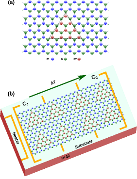
In this article, we study the thermoelectric performance of lateral TMDC heterostructures within a multiscale quantum transport framework with inputs from first-principles calculations. We specifically consider triangular inclusions (see Fig. 1), since 2D TMDCs are typically grown as triangular flakes. We study both -type and -type lateral heterostructures, for all possible combinations of semiconducting TMDC monolayers: MoS2, MoSe2, WS2, and WSe2. -type WS2 with WSe2 triangular inclusions is found to have at room temperature, which is five times larger than the value of pristine -type 1L WS2. The peak room-temperature power factors calculated for lateral TMDC heterostructures here are the highest amongst gapped 2D monolayers reported to date.
I Results
I.1 Nature of scattering in TMDC heterostructures
We calculated thermoelectric properties using the Boltzmann transport theory under the relaxation time approximations. Within this framework, the kinetic definitions of the conductance, Seebeck coefficient, and the electrical thermal conductivity are given by
| (2) | ||||
with
| (3) |
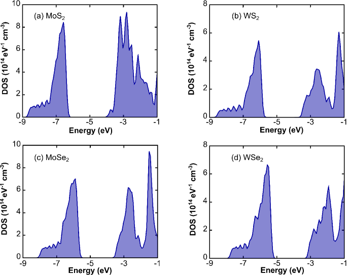
where is the elementary charge, is the density of states, is the carrier velocity, is the Fermi-Dirac distribution function, is the Fermi level, and is the total scattering time. The density of states is extracted from the electronic band structure obtained using the density functional theory (DFT) calculations within the local-density approximations (LDA). Figure 2 displays the density of states as a function of energy for 1L MoS2, WS2, MoSe2 and WSe2. Here, is normalized by the unit-cell area and the corresponding layer thickness. The PF and values are sensitive to the small variations of near the band edges.
To determine , we need to consider both the intrinsic and extrinsic scattering rates. According to the Matthiessen’s law
| (4) |
where is the extrinsic carrier scattering time arising from the material inclusions, and is the total intrinsic scattering time arising from all the acoustic and optical phonon mode contributions. The intrinsic scattering rate is assumed to remain unaltered from the pristine 1L, a commonly used assumption while studying nano-structured thermoelectric materials grossman .
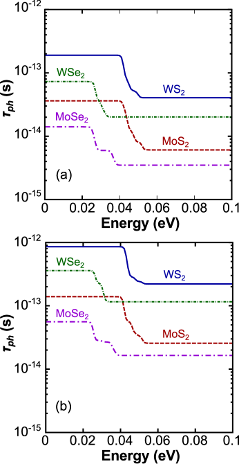
Figure 3 shows the total phonon scattering time versus energy at room temperature for pristine -type and -type 1L TMDCs. We have included the acoustic and optical phonon modes corresponding to the transitions, , via corresponding zeroth and first-order deformation potentials (see Methods for details). The optical phonon modes emerge as steps in the scattering rate. In the family of 1L TMDCs, MoSe2 (WS2) has the strongest (weakest) interaction with phonons. In general, WX2 has a greater phonon-limited electrical conductivity than MoX2. These observations and scattering times are consistent with other first-principles studies reported in the literature Kaasbjerg ; kim_eph .
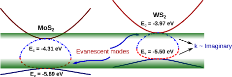
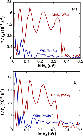
To calculate the carrier scattering time , we have employed a multiscale quantum transport framework informed by first-principles calculations described in Ref. sathwikopendomain . Material inclusions break the translation symmetry of the system. Hence, scattering in these heterostructures can occur via both propagating (real wavevector) and evanescent modes (purely imaginary wavevector). As an example, in Fig. 4, we have plotted the heterointerface formed between 1L MoS2 and WS2. Electronic structure calculations dictate that 1L MoS2 (eV) has a lower conduction band (CB) minimum than 1L WS2 (eV). When an electron in the CB with energy eVeV is injected from 1L MoS2 to WS2, scattering occurs only through the evanescent modes. Similarly, for carriers in the valence band of -type WS2, with energy eVeV (corresponding to the valence band maximum of MoS2) only evanescent modes are available for scattering. Evanescent modes are situated within the bandgap, and result in exponentially decaying contributions to the scattered wavefunction.
Thermoelectric quantities in Eq. (I.1) are directly proportional to the total scattering time . Figure 5 displays the electron scattering rate, , as a function of energy for four different -type material combinations. We see that WS2(MoS2) has a higher scattering time (inverse of the scattering rate) while compared to MoS2(WS2). A similar trend is followed by WSe2(MoSe2) and MoSe2(WSe2) 1L as well.
I.2 Power factor and values in TMDC heterostructures
The main results for the peak power factor and values for the -type and -type TMDC lateral heterostructures are listed in Table 1 and Table 2, respectively. In these tables, the notation A(B) represents that the material B inclusions are confined within the matrix of the material A. The material inclusion is considered here to be an equilateral triangle.
| 1L heterostructure | PF (WK-2m-1) | Pristine 1L (at 300 K) | ||||||||
|---|---|---|---|---|---|---|---|---|---|---|
| A (B) | K | K | K | K | K | K | A | Ozbal | HuangTMD1 | |
| MoS2 (WS2) | 0.365 | 0.293 | 0.181 | 0.093 | 0.124 | 0.125 | MoS2 | 0.25 | 0.22 | 0.25 |
| MoS2 (MoSe2) | 0.335 | 0.256 | 0.167 | 0.084 | 0.109 | 0.115 | MoS2 | 0.25 | 0.22 | 0.25 |
| WS2 (MoS2) | 4.565 | 3.896 | 2.371 | 0.598 | 1.231 | 1.641 | WS2 | 0.20 | 0.22 | 0.23 |
| WS2 (WSe2) | 5.977 | 4.476 | 2.470 | 0.997 | 1.611 | 1.806 | WS2 | 0.20 | 0.22 | 0.23 |
| MoSe2 (WSe2) | 0.500 | 0.367 | 0.200 | 0.173 | 0.227 | 0.205 | MoSe2 | 0.38 | 0.35 | 0.36 |
| MoSe2 (MoS2) | 0.485 | 0.362 | 0.199 | 0.165 | 0.223 | 0.205 | MoSe2 | 0.38 | 0.35 | 0.36 |
| WSe2 (MoSe2) | 1.929 | 1.457 | 0.815 | 0.485 | 0.816 | 0.875 | WSe2 | 0.30 | 0.33 | 0.38 |
| WSe2 (WS2) | 1.954 | 1.468 | 0.819 | 0.488 | 0.821 | 0.879 | WSe2 | 0.30 | 0.33 | 0.38 |
We observe that the -type WS2(WSe2), and -type MoSe2(WSe2) have the maximum values at room temperature. On the other hand, -type WS2(WSe2), -type WS2(MoS2), and -type MoS2(MoSe2) have larger values at higher temperatures. In Tables 1 and 2, for comparison, we have listed the room temperature values for pristine 1L TMDCs obtained from Refs. Ozbal ; HuangTMD1 . For the -type 1L WS2 we observe up to five times larger value with WSe2 inclusions as compared to pristine -type WS2 1L. Similarly, for -type MoSe2 with WSe2 inclusions, we observe an enhancement by a factor of two in the values as compared to pristine 1L MoSe2. In general, values increase with temperature, as there is a multiplicative factor of temperature in Eq. (1).
| 1L heterostructure | PF (WK-2m-1) | Pristine 1L (at 300 K) | ||||||||
|---|---|---|---|---|---|---|---|---|---|---|
| A (B) | K | K | K | K | K | K | A | Ozbal | HuangTMD1 | |
| MoS2 (WS2) | 1.940 | 1.862 | 1.315 | 0.407 | 0.713 | 0.871 | MoS2 | 0.50 | 0.47 | 0.53 |
| MoS2 (MoSe2) | 4.076 | 3.213 | 2.001 | 0.648 | 1.115 | 1.289 | MoS2 | 0.50 | 0.47 | 0.53 |
| WS2 (MoS2) | 0.895 | 0.779 | 0.568 | 0.274 | 0.407 | 0.486 | WS2 | 0.40 | 0.43 | 0.42 |
| WS2 (WSe2) | 1.274 | 1.203 | 0.873 | 0.370 | 0.607 | 0.736 | WS2 | 0.40 | 0.43 | 0.42 |
| MoSe2 (WSe2) | 2.272 | 1.826 | 1.060 | 0.714 | 1.004 | 1.045 | MoSe2 | 0.42 | 0.38 | 0.39 |
| MoSe2 (MoS2) | 2.015 | 1.554 | 0.945 | 0.560 | 0.861 | 0.934 | MoSe2 | 0.42 | 0.38 | 0.39 |
| WSe2 (MoSe2) | 0.034 | 0.023 | 0.014 | 0.015 | 0.017 | 0.016 | WSe2 | 0.35 | 0.34 | 0.35 |
| WSe2 (WS2) | 0.023 | 0.017 | 0.011 | 0.011 | 0.013 | 0.013 | WSe2 | 0.35 | 0.34 | 0.35 |
The calculated peak value of the PF for -type 1L WS2(WSe2) and WS2(MS2) at room temperature is mWK-2m-1 and mWK-2m-1, respectively. These values are about twice the peak PF value observed in the corresponding pristine 1L TMDCs Hippalgaonkar . Moreover, they are of the same order of magnitude as the observed PF in traditional thermoelectric materials, such as Bi2Ti3 (mWK-2m-1 Satterwaithe ) and BiSbTe (mWK-2m-1 Caillat ) crystals.
In Table 1, we observe that -type MoS2(WS2) and MoS2(MoSe2) have significantly lower thermoelectric values compared to a pristine MoS2 1L. Similarly, -type WSe2(WS2) and WSe2(MoSe2) have significantly lower thermoelectric values compared to a pristine WSe2 1L (see Table 2). These phenomena can be explained as a direct consequence of band alignment as explained in the next section.
I.3 Band alignments and the thermoelectric enhancement
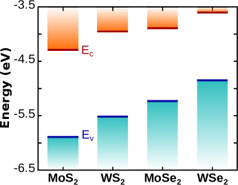
In Fig. 6, we observe that 1L WS2 has a higher CB minimum at the -valley than 1L MoS2. Hence, MoS2 inclusions provide additional conduction channels for electrons entering from the -type 1L WS2. This will increase the electron scattering time as seen in Fig. 5. On the other hand, in the -type MoS2 with WS2 inclusions, scattering occurs through the evanescent modes offered by the WS2 inclusion. This will significantly decrease the scattering time. Moreover, being real functions the evanescent modes indirectly decrease the probability current by draining the probability of propagating channels, thereby, significantly reducing the conductance values.
The total scattering time follows the reciprocal sum rule defined in Eq. (4). Hence, the lower of the two scattering times between and will be the dominating contributor to the thermoelectric quantities. For transport in -type MoS2(WS2) 1L, is an order of magnitude lower than around the band edge. Hence, we obtain low values of PF and values as shown in Table 1.
In -type heterostructures, the valence band (VB) maxima between the two layers determine the occurance of evanescent modes. In Fig. 6, we see that WS2 has a higher VB maximum than MoS2. Thus scattering in the -type WS2(MoS2) occurs through evanescent modes. Hence, we observe that the -type WS2 heterostructures have lower values while compared to the corresponding pristine monolayer as seen in Table 2. Due to additional conduction channels offered by the WS2 inclusions, an enhancement in the and PF values are observed in the -type 1L MoS2(WS2). An analogous mechanism explains the enhancement observed in -type MoSe2(WSe2), which has the highest room temperature value amongst the -type heterostructures.
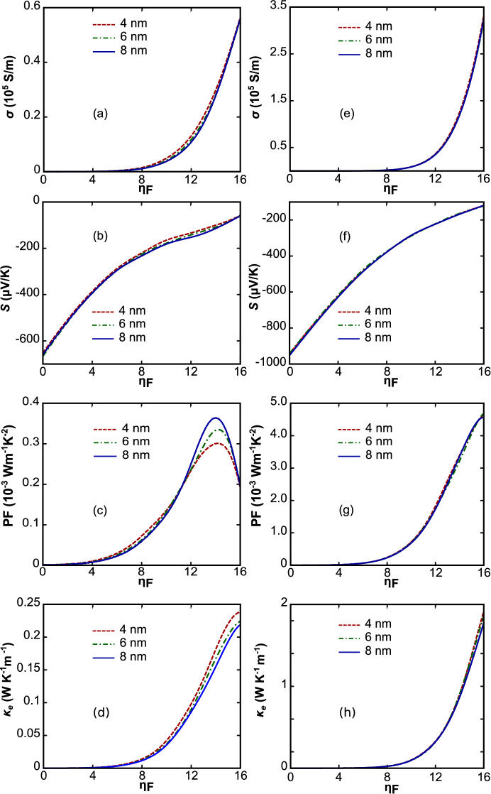
Figure 7 displays the conductance, Seebeck coefficient, PF, and electrical thermal conductivity as a function of the reduced Fermi-level for -type MoS2(WS2), and -type WS2(MoS2) 1L heterostructures. Note that and monotonically increase with . Comparing Fig. 7(a) and (e), we observe a significant enhancement in for WS2(MoS2) as reasoned earlier, whereas the Seebeck coefficient remains of the same order for both the heterostructures. Hence, we obtain high PF and values for the -type 1L WS2(MoS2) heterostructures. A similar trend is followed by other material combinations as well. We note that the PF increases slightly with increase in the width of material inclusions, and we found it to be optimized for the side length of nm for the equilateral triangle inclusions. Unlike Schrödinger particles, the massive Dirac particles in TMDC inclusions have a critical length below which they will not occupy any bound states shenoy . Thus, for inclusions with edges smaller than this critical length, heterostructures considered here will have the thermoelectric values similar to that of 1L pristine.
II Conclusions
In this work, we investigated the thermoelectric properties of semiconducting transition metal dichalcogenide lateral heterostructures using a multiscale quantum transport framework. We reported a new mechanism to enhance the thermoelectric efficiency in 2D materials by adding conduction channels through lateral heterostructures. The -type WS2 monolayer with WSe2 inclusions has the highest room-temperature values, which is about five times larger than the pristine WS2 monolayer. The -type MoSe2 monolayer with WSe2 inclusions is observed to have a room-temperature value about two times larger than the pristine MoSe2 monolayer. The peak PF values calculated in these heterostructures are of the same order of magnitude as traditional high-performance thermoelectric materials such as Bi2Ti3 and BiSbTe. The PF values reported here, are also the highest amongst gapped 2D monolayers. We expect the given mechanism to show similar enhancement of thermoelectric power in oxide and other monolayer heterostructures. Hence, 2D lateral heterostructures provide exciting new avenues to develop ultra-efficient in-plane thermoelectric devices.
III Methods
To determine the thermoelectric quantities in Eq. (I.1) we need to determine the density of states and the total scattering time . The density of states is computed from DFT calculations. The phonon and electron scattering contributions of are determined independently.
DFT calculations were performed, using the Vienna Ab Initio Simulation Package (VASP) kresse1 ; kresse2 , to obtain the density of states for the various TMDC monolayers studied here. Core and valence electrons were modeled using the projector-augmented wave (PAW) method blochl ; kresse3 and the local density approximation ceperley ; perdew was used to describe electron exchange and correlation. The kinetic energy cutoff was set to eV and a Gaussian smearing of eV was used for Brillouin-zone integrations. The Brillouin zones were sampled using an -centered -point mesh. The lattice parameters for the TMDC monolayers were fixed at the bulk experimental parameters (MoS2: moss ; MoSe2: lavik ; WS2 & WSe2: schutte ). As semilocal functionals underestimate the fundamental gaps of semiconductors, the density of states were shifted, a posteriori, to match the quasiparticle gaps reported in Ref. C2DB .
The deformation potentials obtained from first-principles calculations Kaasbjerg ; kim_eph were employed to compute both the acoustic and optical phonon mode contributions. We have included the zeroth order acoustic and optical, and first order acoustic mode contributions. The effect of the Fröhlich interaction is implicitly added to the deformation potential kim_eph . The total is determined using the reciprocal sum of these contributions as prescribed by Matthiessen’s law. Further details of these calculations can be found in Ref. sathwikopendomain .
For elastic scattering processes in 2D, the kinetic definition of is given by where is the disorder density, is the average velocity, and is the momentum scattering cross-section. for a uniform incoming velocity distribution. is determined using a multiscale quantum transport framework sathwikopendomain . Carrier scattering in lateral heterostructures occurs via both propagating and evanescent modes. Standard scattering calculations cannot account for these crucial contributions of decaying evanescent modes, since their probabilities vanish at the asymptotic limit, where the boundary conditions are applied to determine the scattering amplitudes. On the other hand, our methodology accurately includes these contributions since we have circumvented the need for the asymptotic boundary conditions by introducing absorbers around the scattering centers.
| (eV) | (eV) | (Å) | (eV) | (eV) | eVÅ2 | () | () | ||
|---|---|---|---|---|---|---|---|---|---|
| MoS2 | -4.31 | -5.89 | 3.184 | 1.059 | 0.073 | -5.97(-6.43) | 0.45 | 0.53 | |
| WS2 | -5.97 | -5.50 | 3.186 | 1.075 | 0.211 | -6.14(-7.95) | 0.3 | 0.34 | |
| MoSe2 | -3.91 | -5.23 | 3.283 | 0.940 | 0.090 | -5.34(-5.71) | 0.53 | 0.58 | |
| WSe2 | -3.61 | -4.85 | 3.297 | 1.190 | 0.230 | -5.25(-6.93) | 0.33 | 0.36 |
Scattering properties are determined through a -band Hamiltonian of the form
| (5) |
where denotes the Pauli matrices, is the lattice constant, is the effective hopping integral, is the spin-orbit (SO) parameter, and is given by
| (6) |
Here, is a material parameter, and and are the CB minimum and the VB maximum at the -valley, respectively. All the material parameters employed in this article are listed in Table 3. A detailed discussion of the quantum transport framework employed here is described in Ref. sathwikopendomain . The quantum transport calculations combined with the Boltzmann transport theory determine , and (see Eq. (I.1)). To determine the factor we also require the phonon thermal conductivity (see Eq. (1)). Typically is computed through the phonon dispersion relations. We have utilized the values listed in Ref. Ozbal , that are obtained using DFT calculations.
Acknowledgements.
Calculations presented here were performed using computational resources supported by the Academic and Research Computing Group at WPI.References
- (1) M. S. Dresselhaus, G. Chen, M. Y. Tang, R. G. Yang, H. Lee, D. Z. Wang, Z. F. Ren, J. P. Fleurial, P. Gogna, New Directions for Low-Dimensional Thermoelectric Materials, Adv. Mater. 19, 1043–1053 (2007).
- (2) G. Chen, M. S. Dresselhaus, G. Dresselhaus, J. P. Fleurial, and T. Caillat, Recent developments in thermoelectric materials, International Materials Reviews 48, 45–66 (2003).
- (3) C. J. Vineis, A. Shakouri, A. Majumdar, and M. G. Kanatzidis, Nanostructured Thermoelectrics: Big Efficiency Gains from Small Features, Adv. Mater. 22, 3970–3980 (2010).
- (4) R. Franz and G. Wiedemann, Über die Wärme-Leitungsfähigkeit der Metalle, Annalen der Physik 165, 497–531 (1853).
- (5) D. M. Rowe, Thermoelectrics Handbook: Macro to Nano, (CRC Press, Boca Raton, Florida, 2005).
- (6) L. D. Hicks and M. S. Dresselhaus, Thermoelectric figure of merit of a one-dimensional conductor, Phys. Rev. B 47, 16631–16634 (1993).
- (7) L. D. Hicks and M. S. Dresselhaus, Effect of quantum-well structures on the thermoelectric figure of merit, Phys. Rev. B 47, 12727-12731 (1993).
- (8) L. D. Hicks, T. C. Harman, X. Sun and M. S. Dresselhaus, Experimental study of the effect of quantum-well structures on the thermoelectric figure of merit, Phys. Rev. B 53, R10493–R10496 (1996).
- (9) N. T. Hung, E. H. Hasdeo, A. R. T. Nugraha, M. S. Dresselhaus and R. Saito, Quantum Effects in the Thermoelectric Power Factor of Low-Dimensional Semiconductors, Phys. Rev. Lett. 117, 036602 (2016).
- (10) A. Majumdar, Thermoelectricity in Semiconductor Nanostructures, Science 303, 777–778 (2004) .
- (11) Y. Pei, H. Wang and G.J. Snyder, Band Engineering of Thermoelectric Materials, Adv. Mater. 24, 6125–6135 (2012).
- (12) T. Koga, X. Sun, S. B. Cronin, and M. S. Dresselhaus, Carrier pocket engineering to design superior thermoelectric materials using GaAs/AlAs superlattices, Appl. Phys. Lett. 73, 2950–2952 (1998).
- (13) J.-H. Bahk, Z. Bian, and A. Shakouri, Electron energy filtering by a nonplanar potential to enhance the thermoelectric power factor in bulk materials, Phys. Rev. B 87, 075204 (2013).
- (14) Y.-M. Lin, O. Rabin, S. B. Cronin, J. Y. Ying, and M. S. Dresselhaus, Semimetal–semiconductor transition in Bi(1-x)Sbx alloy nanowires and their thermoelectric properties, Appl. Phys. Lett. 81, 2403–2405 (2002).
- (15) M. Zebarjadi, An Overview of 2D Materials for Thermoelectric Applications, Celebrating Millie (2018). Available from: https://millie.pubpub.org/pub/b0fn884z
- (16) F. Bonaccorso, L. Colombo, G. Yu, M. Stoller, V. Tozzini, A. C. Ferrari, R. S. Ruoff, and V. Pellegrini, Graphene, related two-dimensional crystals, and hybrid systems for energy conversion and storage, Science 347, 1246501 (2015).
- (17) J. Duan, X. Wang, X. Lai, G. Li, K. Watanabe, T. Taniguchi, M. Zebarjadi, and E. Y. Andrei, High thermoelectric power factor in graphene/hBN devices, Proc. Natl Acad. Sci. 113, 14272–14276 (2016).
- (18) S. Chen, A.L. Moore, W. Cai, J.W. Suk, J. An, C. Mishra, C. Amos, C.W. Magnuson, J. Kang, L. Shi, and R.S. Ruoff, Raman Measurements of Thermal Transport in Suspended Monolayer Graphene of Variable Sizes in Vacuum and Gaseous Environments, ACS Nano 5, 321 (2010).
- (19) S. Chen, Q. Wu, C. Mishra, J. Kang, H. Zhang, K. Cho, W. Cai, A.A. Balandin, R.S. Ruoff, Thermal conductivity of isotopically modified graphene, Nat Mater 11, 203 (2012).
- (20) Y. Cai, J. Lan, G. Zhang, and Y.-W. Zhang, Lattice vibrational modes and phonon thermal conductivity of monolayer MoS2, Phys. Rev. B 89, 035438 (2014).
- (21) G. Ozbal , R. T. Senger, C. Sevik, and H. Sevincli, Ballistic thermoelectric properties of monolayer semiconducting transition metal dichalcogenides and oxides, Phys. Rev. B 100, 085415 (2019).
- (22) W. Huang, H. Da, and G. Liang, Thermoelectric performance of MX2 (M: Mo,W; X: S,Se) monolayers, J. Appl. Phys. 113, 104304 (2013).
- (23) W. Huang, X. Luo, C. K. Gan, S. Y. Quek, and G. Liang, Theoretical study of thermoelectric properties of few-layer MoS2 and WSe2, Phys. Chem. Chem. Phys. 16, 10866 (2014).
- (24) D. Wickramaratne, F. Zahid, and R. K. Lake, Electronic and thermoelectric properties of few-layer transition metal dichalcogenides, J. Chem. Phys. 140, 124710 (2014).
- (25) H. Babaei, J. M. Khodadadi, and S. Sinha, Large theoretical thermoelectric power factor of suspended single-layer MoS2, Appl. Phys. Lett. 105, 193901 (2014).
- (26) B. Ouyang, S. Chen, Y. Jing, T. Wei, S. Xiong, and D. Donadio, Enhanced thermoelectric performance of two dimensional MS2 (M = Mo, W) through phase engineering, J. Materiomics 4, 329–337 (2018).
- (27) K. Hippalgaonkar, Y. Wang, Y. Ye, D. Y. Qiu, H. Zhu, Y. Wang, J. Moore, S. G. Louie, and X. Zhang, High thermoelectric power factor in two-dimensional crystals of Mo, Phys. Rev. B 95, 115407 (2017).
- (28) T. Zhu, K. Swaminathan-Gopalan, K. Stephani, and E. Ertekin, Thermoelectric phonon-glass electron-crystal via ion beam patterning of silicon, Phys. Rev. B 97, 174201 (2018).
- (29) M. Kayyalha, J. Maassen, M. Lundstrom, L. Shi, and Y. P. Chen, Gate-tunable and thickness-dependent electronic and thermoelectric transport in few-layer MoS2, J. Appl. Phys. 120, 134305 (2016).
- (30) X. Duan, C. Wang, J. C. Shaw, R. Cheng, Y. Chen, H. Li, X. Wu, Y. Tang, Q. Zhang, A. Pan, J. Jiang, R. Yu, Y. Huang, and X. Duan, Lateral epitaxial growth of two-dimensional layered semiconductor heterojunctions, Nat. Nanotechnol. 9, 1024 (2014).
- (31) X.-Q. Zhang, C.-H. Lin, Y.-W. Tseng, K.-H. Huang, and Y.-H. Lee, Synthesis of Lateral Heterostructures of Semiconducting Atomic Layers, Nano Lett. 15, 410 (2015).
- (32) M.-Y. Li, Y. Shi, C.-C. Cheng, L.-S. Lu, Y.-C. Lin, H.-L. Tang, M.-L. Tsai, C.-W. Chu, K.-H. Wei, J.-H. He, W.-H. Chang, K. Suenaga, and L.-J. Li, Epitaxial growth of a monolayer WSe2-MoS2 lateral p-n junction with an atomically sharp interface, Science 349, 524 (2015).
- (33) C. Zhang, Y. Chen, J.-K. Huang, X. Wu, L.-J. Li, W. Yao, J. Tersoff, and C.-K. Shih, Visualizing band offsets and edge states in bilayer–monolayer transition metal dichalcogenides lateral heterojunction, Nat. Commun. 7, 10349 (2016).
- (34) C. Zhang, M.-Y. Li, J. Tersoff, Y. Han, Y. Su, L.-J. Li, D. A. Muller, and C.-K. Shih, Strain distributions and their influence on electronic structures of WSe2–MoS2 laterally strained heterojunctions, Nat. Nanotechnol. 13, 152 (2018).
- (35) P. K. Sahoo, S. Memaran, Y. Xin, L. Balicas, and H. R. Gutiérrez, One-pot growth of two-dimensional lateral heterostructures via sequential edge-epitaxy, Nature 553, 63 (2018).
- (36) S. Xie, L. Tu, Y. Han, L. Huang, K. Kang, K. U. Lao, P. Poddar, C. Park, D. A. Muller, R. A. DiStasio, and J. Park, Coherent, atomically thin transition-metal dichalcogenide superlattices with engineered strain, Science 359, 1131 (2018).
- (37) Y. Zhang, and G. D. Stucky, Heterostructured Approaches to Efficient Thermoelectric Materials, Chem. Mater. 26, 837–848 (2014).
- (38) R. Venkatasubramanian, E. Siivola, T. Colpitts, and B. O’Quinn, Thin-film thermoelectric devices with high room-temperature figures of merit, Nature 413, 597 (2001).
- (39) S. Haastrup, M. Strange, M. Pandey, T. Deilmann, P. S. Schmidt, N. F. Hinsche, M. N. Gjerding, D. Torelli, P. M. Larsen, A. C. Riis-Jensen, J. Gath, K. W. Jacobsen, J. J. Mortensen, T. Olsen, K. S. Thygesen, The Computational 2D Materials Database: High-Throughput Modeling and Discovery of Atomically Thin Crystals, 2D Materials 5, 042002 (2018).
- (40) K. Kaasbjerg, K. S. Thygesen, and K. W. Jacobsen, Phonon-limited mobility in n-type single-layer MoS2 from first principles, Phys. Rev. B 85, 115317 (2012).
- (41) Z. Jin, X. Li, J. T. Mullen, and K. W. Kim, Intrinsic transport properties of electrons and holes in monolayer transition-metal dichalcogenides, Phys. Rev. B 90, 045422 (2014).
- (42) X. Li, J. T. Mullen, Z. Jin, K. M. Borysenko, M. B. Nardelli, and K. W. Kim, Intrinsic electrical transport properties of monolayer silicene and MoS2 from first principles, Phys. Rev. B 87, 115418 (2013).
- (43) A. Kormányos, G. Burkard, M. Gmitra, J. Fabian, V. Zólyomi, N. D. Drummond, and V. I. Fal’ko, kp theory for two-dimensional transition metal dichalcogenide semiconductors, 2D Mater. 2, 022001 (2015).
- (44) C. Satterwaithe and R. Ure JR., Electrical and Thermal Properties of Bi2Te3 Phys. Rev. 108, 1164–1170 (1957).
- (45) T. Caillat, M. Carle, P. Pierrat, H. Scherrer, and S. Scherrer, Thermoelectric properties of BixSbTe3 single crystal solid solutions grown by the T.H.M. method, J. Phys. Chem. Solids 53, 1121 (1992).
- (46) J.-H. Lee, G. A. Galli, and J. C. Grossman, Nanoporous Si as an Efficient Thermoelectric Material, Nano Lett. 8, 3750 (2008).
- (47) Sathwik Bharadwaj, Ashwin Ramasubramaniam, and L. R. Ram-Mohan (Submitted for publication).
- (48) C. C. Price, N. C. Frey, D. Jariwala, and V. B. Shenoy, Engineering Zero-Dimensional Quantum Confinement in Transition-Metal Dichalcogenide Heterostructures, ACS Nano 13, 8303-8311 (2019).
- (49) G. Kresse, J. Furthmüller, Efficiency of Ab-Initio Total Energy Calculations for Metals and Semiconductors Using a Plane-Wave Basis Set, Comput. Mater. Sci. 6, 15–50 (1996)
- (50) G. Kresse, J. Furthmüller, Efficient Iterative Schemes for Ab Initio Total-Energy Calculations Using a Plane-Wave Basis Set Phys. Rev. B 54, 11169–11186 (1996)
- (51) P. E. Blöchl, Projector Augmented-Wave Method Phys. Rev. B 50, 17953–17979 (1994)
- (52) G. Kresse, D. Joubert, From Ultrasoft Pseudopotentials to the Projector Augmented-Wave Method Phys. Rev. B 59, 1758–1775 (1999)
- (53) D. M. Ceperley and B. J. Alder, Ground State of the Electron Gas by a Stochastic Method, Phys. Rev. Lett. 45, 566 (1980).
- (54) J. P. Perdew and A. Zunger, Self-interaction correction to density-functional approximations for many-electron systems, Phys. Rev. B 23, 5048 (1981).
- (55) B. Schönfeld, J. J. Huang, and S. C. Moss, Anisotropic mean‐square displacements (MSD) in single‐crystals of 2H‐ and 3R‐MoS2 Acta Cryst. B39, 404–407 (1983).
- (56) P. B. James and M. T. Lavik, The crystal structure of MoSe2, Acta Cryst. 16, 1183 (1963).
- (57) W. J. Schutte, J. L. De Boer, F. Jellinek, Crystal structures of tungsten disulfide and diselenide, J. Solid State Chem. 70, 207–209 (1987).