Engineered magnetization and exchange stiffness in direct-write Co-Fe nanoelements
Abstract
Media with engineered magnetization are essential building blocks in superconductivity, magnetism and magnon spintronics. However, the established thin-film and lithographic techniques insufficiently suit the realization of planar components with on-demand-tailored magnetization in the lateral dimension. Here, we demonstrate the engineering of the magnetic properties of CoFe-based nanodisks fabricated by the mask-less technique of focused electron beam induced deposition (FEBID). The material composition in the nanodisks is tuned in-situ via the e-beam waiting time in the FEBID process and their post-growth irradiation with Ga ions. The magnetization and exchange stiffness of the disks are deduced from perpendicular ferromagnetic resonance measurements. The achieved variation in the broad range from emu/cm3 to emu/cm3 continuously bridges the gap between the values of such widely used magnonic materials as permalloy and CoFeB. The presented approach paves a way towards nanoscale 2D and 3D systems with controllable and space-varied magnetic properties.
Magnonics – the study of spin waves and their use in information processing systems – has emerged as one of the most rapidly developing research fields of modern magnetism Kruglyak, Demokritov, and Grundler (2010); Demokritov and Slavin (2013); Chumak et al. (2015); Wagner et al. (2016); Dobrovolskiy et al. (2019a); Tsymbal and Zutic (2019); Gubbiotti (2019); Mahmoud et al. (2020); Wang et al. (2020); Li et al. (2020). The key challenges in modern magnonics are guiding and control of spin waves in 1D (e.g., magnonic crystals Krawczyk and Grundler (2014); Kakazei et al. (2014); Chumak, Serga, and Hillebrands (2017); Zakeri (2020)), 2D (e.g., magnonic circuits Mahmoud et al. (2020); Wang et al. (2020)), and emerging 3D systems Krawczyk and Puszkarski (2008); Yan et al. (2011); Gubbiotti (2019). For steering of spin waves, one should change an external parameter such as magnetic field Chumak et al. (2009); Liu et al. (2013); Golovchanskiy et al. (2018); Dobrovolskiy et al. (2019a), temperature Polushkin et al. (2012); Dzyapko et al. (2016); Vogel et al. (2018) or alter the conduit shape Krawczyk and Grundler (2014); Gruszecki and Krawczyk (2018); Dobrovolskiy et al. (2019b) and magnetization Baumgaertl, Watanabe, and Grundler (2018); Davies et al. (2015); Vogel et al. (2018); Whitehead et al. (2019); Bali et al. (2014); Urbanek et al. (2018). Variations of temperature and field have drawbacks of being energy-consuming, and their localized application is challenging to implement. A shape variation is free of these complications but it usually involves multiple nanofabrication steps and allows one to only coarsely alter the magnetization between the given material’s value and zero in regions where no material is present. Among these approaches, magnetization variation has an advantage if being passive (no current or heat involved) and it can be strongly localized or gradient-tailored on purpose. Thus, in-situ approaches for tuning magnetization in a broad range are strongly demanded.
In this regard, focused electron beam induced deposition (FEBID) can offer unique features which go beyond the state-of-the-art fabrication technologies of magnonics Huth, Porrati, and Dobrovolskiy (2018). Firstly, the down to nm lateral resolution (for selected materials, such as Co-Fe alloys Porrati et al. (2015) used here) makes FEBID suitable for the fabrication of nanostructures with feature sizes comparable to modern complementary metal-oxide semiconducting (CMOS) technology. Secondly, the composition and magnetic properties of FEBID nanostructures can be tuned in-situ by altering the writing strategy and via post-growth irradiation of structures with ions Lara et al. (2014); Dobrovolskiy et al. (2019b) and electrons Dobrovolskiy et al. (2015). In addition, FEBID is capable to fabricate complex-shaped 3D nano-architectures Fernandez-Pacheco et al. (2020); Porrati et al. (2019), that make it the technique of choice for studies in superconductivity Dobrovolskiy et al. (2011, 2018, 2019c), magnetism Fernández-Pacheco et al. (2017); Streubel et al. (2016); Sheka et al. (2020) and magnonics Krawczyk and Puszkarski (2008); Yan et al. (2011); Gubbiotti (2019).
In a previous study, we observed the decrease of the magnetization and the exchange stiffness with reduction of the diameter of individual Co-Fe nanodisks Dobrovolskiy et al. (2020). The effect was attributed to the writing of smaller disks in a depleted-precursor regime which results in a lower metal content. Here, we use this effect to demonstrate on-demand engineering of the magnetization and exchange stiffness in individual Co-Fe nanodisks with a fixed radius nm and thickness nm. Specifically, one series of nanodisks was fabricated using different e-beam waiting times in the FEBID process and another series of nanodisks was irradiated with different doses of Ga ions. The magnetization and exchange stiffness of the disks were deduced from ferromagnetic resonance (FMR) measurements, employing a recently developed spatially-resolved approach Dobrovolskiy et al. (2020). We demonstrate that with an increase of the e-beam waiting time, of the disks reaches emu/cm3, which is by a factor of two larger than of the disks irradiated with Ga ions. Thus, the combination of these two approaches provides access to the fabrication of geometrically uniform magnonic conduits with a drastic variation of saturation magnetization.
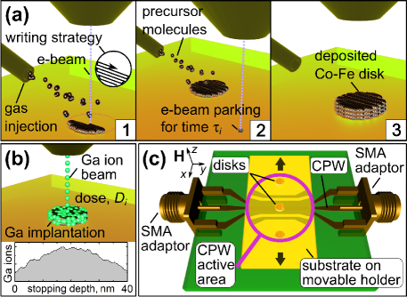
The circular Co-Fe disks were fabricated by FEBID in a high-resolution dual-beam scanning electron microscope (SEM: FEI Nova NanoLab 600) employing HCo3Fe(CO)12 as precursor gas Porrati et al. (2015); Kumar T. P. et al. (2018). Two series of samples were fabricated. The first series of samples is a set of four disks deposited onto a Si/SiO2 (200 nm) substrate, written with different beam waiting times. Namely, after each pass of the electron beam over the disk surface, the beam was “parked” for the time varied from to ms outside of the disk. The essential steps of the writing process are illustrated in Fig. 1(a). The substrate with the disks was mounted onto a translational stage for their face-to-face positioning under the m-wide and m-long active part of an Au coplanar waveguide (CPW), Fig. 1(c). The CPW was prepared by e-beam lithography from a nm-thick Au film dc-magnetron-sputtered onto a Si/SiO2 (200 nm) substrate with a nm-thick Cr buffer layer. The CPW was covered with a nm-thick TiO2 layer for electrical insulation from the disks.
The second series of samples refers to four measurements of a disk written with on the CPW and irradiated with keV Ga ions up to a cumulative dose of pC/m2 in steps of pC/m2, Fig. 1(b). SRIM simulations of the distribution of keV Ga ions implanted in the Co-Fe disks indicate that it has a gentle-dome shape spreading through the entire disk thickness, with the largest number of stopped Ga ions in the depth range from nm to nm, see the inset in Fig. 1(b). Ferromagnetic resonance measurements on both sample series were taken at the fixed frequency GHz with magnetic field oriented perpendicularly to the disk plane, Fig. 1(c).
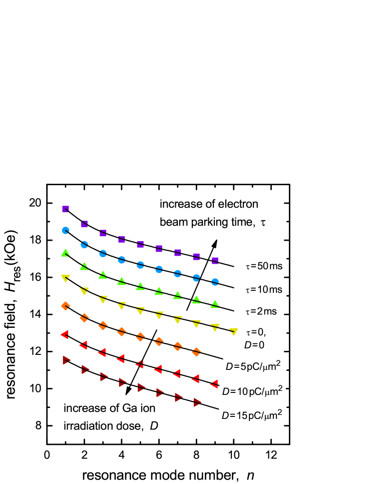
For the analytical description of the field values of resonance peaks, we considered azimuthally symmetric spin-wave modes in a thin cylindrical ferromagnetic disk saturated in the out-of-plane direction by the biasing magnetic field . In this case, the excited spin-wave eigenmodes can be described by Bessel functions of the zeroth order because of the axial symmetry of the samples. Details of the analytical theory can be found elsewhere Kakazei et al. (2004). This approach allows for the deduction of and with high precision.
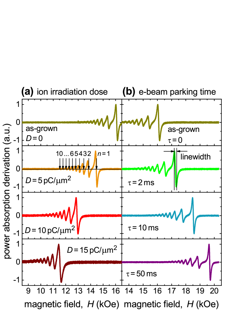
Figure 2 presents the experimentally measured spin-wave resonance spectra as a function of the out-of-plane magnetic field for the disks irradiated with different doses of Ga ions and the disks deposited with different electron beam waiting times. In all cases the most intense resonance peak is observed at the largest field that corresponds to the lowest spin-wave mode number . On the low-field side, the main resonance is accompanied by a series of peaks with a monotonously decreasing amplitude. Such a spin-wave spectrum is typical for confined circular nanodots Kakazei et al. (2004). We observe that the two used approaches lead to shifts of the spin-wave resonance fields in opposite directions with respect to the reference state (, ). At the same time, the shape and the intermodal distance pattern evolve consistently which is indicative of compositional uniformity and magnetic homogeneity of the samples. After integration and subtraction of the background, the experimental spectra were compared with multipeak Lorentzian functions to obtain the resonance fields for each mode. A theoretical model Kakazei et al. (2004) was applied to fit the experimental data using and as two fitting parameters and assuming the gyromagnetic ratio of MHz/Oe Tokac et al. (2015). The application of a least-square algorithm allowed us to deduce the magnetic parameters for all individual nanodisks with a precision of about %. Figure 3 illustrates that the best theoretical fits (solid lines) nicely describe the experimental data (symbols). We note that the location of the main resonance peak is primarily determined by . The value of only weakly affects the position of the main resonance peak, however, it strongly affects the positions of the higher-order peaks.
The deduced and values are reported in Fig. 4(a,b). The field-sweep FMR linewidth, determined as the peak-to-peak distance in Fig. 2(b), is presented in Fig. 4(c). We next analyze their evolution in comparison with the composition of the disks inferred from energy-dispersive x-ray (EDX) spectroscopy. The EDX data in Fig. 4(d) reveal an increase of the [Co+Fe] content from about at. in the as-grown sample () to about for the sample written with the beam parking time ms, Fig. 4(d). We attribute the increase of the metal content in the disk written with ms to a nearly precursor depletion-free mode during its deposition, as the electron beam parking on such a timescale allows the precursor to replenish. The increase of the metal content correlates well with the increase of and and the decrease of the linewidth in Fig. 4. In contrast, irradiation with Ga ions causes a degradation of the magnetic properties of the nanodisks, leading to a reduction of and , and an increase of the linewidth.
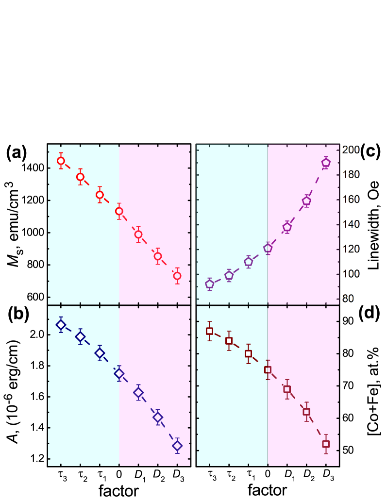
The particular values of and were chosen as a scale factor in Fig. 4 to demonstrate in one plot the opposite character of the used approaches and the whole tuning range of and for Co-Fe nanostructures. The data in Fig. 4(a) suggest that can be varied by a factor of about two, which offers sufficient flexibility, e.g. for the design of graded-index magnonic conduits Davies et al. (2015); Whitehead et al. (2019); Gruszecki and Krawczyk (2018) and magnonic crystals Krawczyk and Grundler (2014); Chumak, Serga, and Hillebrands (2017); Zakeri (2020). The data in Fig. 4(c,d) indicate that a decrease of the metal content in the disks by about at.% is accompanied by a factor-of-two linewidth broadening. Yet, we note that the linewidth ( Oe at 9.85 GHz) in the most CoFe-rich disk is a factor of about two larger than in sputtered Py films Kalarickal et al. (2006).
To summarize, we have demonstrated a methodology for the magnetization and exchange stiffness engineering in Co-Fe micrometer-sized nanodisks. The disks were fabricated by the direct-write nanofabrication technology of focused electron beam induced deposition. The analysis of the perpendicular FMR measurements data revealed an increase of the magnetization and the exchange stiffness in the disks written with longer e-beam waiting time and a reduction of and in disks irradiated with Ga ions. The physical reason for the larger and is the operation of FEBID in a nearly depletion-free precursor regime, which results in a higher metal content and smaller damping (which is proportional to the FMR linewidth) in the disks. The decrease of and in conjunction with the linewidth increase reflects a degradation of the magnetic properties and a higher inhomogeneity of the disks irradiated with Ga ions. Specifically, the achieved variation of from about emu/cm3 to about emu/cm3 allows for its engineering in a broad range, continuously bridging the gap between the values of such widely used magnonic materials as Py and CoFeB Chumak, Serga, and Hillebrands (2017). The tuning is accompanied by a variation of the exchange stiffness in the range erg/cm to erg/cm and the field-sweep FMR linewidth between Oe and Oe. The reported approach opens a way towards nanoscale 2D and 3D systems with controllable and space-varying magnetic properties.
OVD acknowledges the Austrian Science Fund (FWF) for support through Grant No. I 4889 (CurviMag). The Portuguese team acknowledges the Network of Extreme Conditions Laboratories-NECL and Portuguese Foundation of Science and Technology (FCT) support through Project Nos. NORTE-01-0145-FEDER-022096, POCI-0145-FEDER-030085 (NOVAMAG), and EXPL/IF/00541/2015. BB acknowledges financial support by the Vienna Doctoral School in Physics (VDSP). KL and AVC acknowledge the Austrian Science Fund (FWF) for support through Grant No. I 4696. KG acknowledges support by IKERBASQUE (the Basque Foundation for Science). The work of KG was supported by the Spanish Ministerio de Ciencia, Innovacion y Universidades grant FIS2016-78591-C3-3-R. AVC and QW acknowledge support within the ERC Starting Grant no. 678309 MagnonCircuits. Support through the Frankfurt Center of Electron Microscopy (FCEM) is gratefully acknowledged.
References
- Kruglyak, Demokritov, and Grundler (2010) V. V. Kruglyak, S. O. Demokritov, and D. Grundler, J. Phys. D 43, 264001 (2010).
- Demokritov and Slavin (2013) S. O. Demokritov and A. N. Slavin, eds., Magnonics (Springer Berlin Heidelberg, 2013).
- Chumak et al. (2015) A. V. Chumak, V. I. Vasyuchka, A. A. Serga, and B. Hillebrands, Nat. Phys. 11, 453 (2015).
- Wagner et al. (2016) K. Wagner, A. Kákay, K. Schultheiss, A. Henschke, T. Sebastian, and H. Schultheiss, Nat. Nanotechnol. 11, 432 (2016).
- Dobrovolskiy et al. (2019a) O. V. Dobrovolskiy, R. Sachser, T. Brächer, T. Böttcher, V. V. Kruglyak, R. V. Vovk, V. A. Shklovskij, M. Huth, B. Hillebrands, and A. V. Chumak, Nat. Phys. 15, 477 (2019a).
- Tsymbal and Zutic (2019) E. Tsymbal and I. Zutic, eds., Spintronics Handbook: Spin Transport and Magnetism (CRC Press, Boca Raton, Florida, 2019).
- Gubbiotti (2019) G. Gubbiotti, ed., Three-Dimensional Magnonics: Layered, Micro- and Nanostructures (Jenny Stanford Publishing, 2019).
- Mahmoud et al. (2020) A. Mahmoud, F. Ciubotaru, F. Vanderveken, A. V. Chumak, S. Hamdioui, C. Adelmann, and S. Cotofana, J. Appl. Phys. 128, 161101 (2020).
- Wang et al. (2020) Q. Wang, M. Kewenig, M. Schneider, R. Verba, F. Kohl, B. Heinz, M. Geilen, M. Mohseni, B. Lägel, F. Ciubotaru, C. Adelmann, C. Dubs, S. D. Cotofana, O. V. Dobrovolskiy, T. Brächer, P. Pirro, and A. V. Chumak, Nature Electron. (2020), 10.1038/s41928-020-00485-6.
- Li et al. (2020) Y. Li, W. Zhang, V. Tyberkevych, W.-K. Kwok, A. Hoffmann, and V. Novosad, J. Appl. Phys. 128, 130902 (2020).
- Krawczyk and Grundler (2014) M. Krawczyk and D. Grundler, J. Phys.: Condens. Matt. 26, 123202 (2014).
- Kakazei et al. (2014) G. N. Kakazei, X. M. Liu, J. Ding, and A. O. Adeyeye, Appl. Phys. Lett. 104, 042403 (2014).
- Chumak, Serga, and Hillebrands (2017) A. V. Chumak, A. A. Serga, and B. Hillebrands, J. Phys. D: Appl. Phys. 50, 244001 (2017).
- Zakeri (2020) H. Zakeri, J. Phys. Cond. Matt. 32, 363001 (2020).
- Krawczyk and Puszkarski (2008) M. Krawczyk and H. Puszkarski, Phys. Rev. B 77, 054437 (2008).
- Yan et al. (2011) M. Yan, C. Andreas, A. Kakay, F. Garcia-Sanchez, and R. Hertel, Appl. Phys. Lett. 99, 122505 (2011).
- Chumak et al. (2009) A. V. Chumak, T. Neumann, A. A. Serga, B. Hillebrands, and M. P. Kostylev, J. Phys. D: Appl. Phys. 42, 205005 (2009).
- Liu et al. (2013) X. M. Liu, J. Ding, G. N. Kakazei, and A. O. Adeyeye, Appl. Phys. Lett. 103, 062401 (2013).
- Golovchanskiy et al. (2018) I. A. Golovchanskiy, N. N. Abramov, V. S. Stolyarov, V. V. Bolginov, V. V. Ryazanov, A. A. Golubov, and A. V. Ustinov, Adv. Func. Mater. 28, 1802375 (2018).
- Polushkin et al. (2012) N. I. Polushkin, V. Oliveira, O. Conde, R. Vilar, Y. N. Drozdov, A. Apolinário, A. García-García, J. M. Teixeira, and G. N. Kakazei, Appl. Phys. Lett. 101, 132408 (2012).
- Dzyapko et al. (2016) O. Dzyapko, I. V. Borisenko, V. E. Demidov, W. Pernice, and S. O. Demokritov, Appl. Phys. Lett. 109, 232407 (2016).
- Vogel et al. (2018) M. Vogel, R. Aßmann, P. Pirro, A. V. Chumak, B. Hillebrands, and G. von Freymann, Sci. Rep. 8, 11099 (2018).
- Gruszecki and Krawczyk (2018) P. Gruszecki and M. Krawczyk, Phys. Rev. B 97, 094424 (2018).
- Dobrovolskiy et al. (2019b) O. V. Dobrovolskiy, R. Sachser, S. A. Bunyaev, D. Navas, V. M. Bevz, M. Zelent, W. Smigaj, J. Rychly, M. Krawczyk, R. V. Vovk, M. Huth, and G. N. Kakazei, ACS Appl. Mater. Interf. 11, 17654 (2019b).
- Baumgaertl, Watanabe, and Grundler (2018) K. Baumgaertl, S. Watanabe, and D. Grundler, Appl. Phys. Lett. 112, 142405 (2018).
- Davies et al. (2015) C. S. Davies, A. Francis, A. V. Sadovnikov, S. V. Chertopalov, M. T. Bryan, S. V. Grishin, D. A. Allwood, Y. P. Sharaevskii, S. A. Nikitov, and V. V. Kruglyak, Phys. Rev. B 92, 020408 (2015).
- Whitehead et al. (2019) N. J. Whitehead, S. A. R. Horsley, T. G. Philbin, and V. V. Kruglyak, Phys. Rev. B 100, 094404 (2019).
- Bali et al. (2014) R. Bali, S. Wintz, F. Meutzner, R. Hübner, R. Boucher, A. A. Ünal, S. Valencia, A. Neudert, K. Potzger, J. Bauch, F. Kronast, S. Facsko, J. Lindner, and J. Fassbender, Nano Lett. 14, 435 (2014).
- Urbanek et al. (2018) M. Urbanek, L. Flajsman, V. Krizakova, J. Gloss, M. Horky, M. Schmid, and P. Varga, APL Mater. 6, 060701 (2018).
- Huth, Porrati, and Dobrovolskiy (2018) M. Huth, F. Porrati, and O. V. Dobrovolskiy, Microelectr. Engin. 185-186, 9 (2018).
- Porrati et al. (2015) F. Porrati, M. Pohlit, J. Müller, S. Barth, F. Biegger, C. Gspan, H. Plank, and M. Huth, Nanotechnol. 26, 475701 (2015).
- Lara et al. (2014) A. Lara, O. V. Dobrovolskiy, J. L. Prieto, M. Huth, and F. G. Aliev, Appl. Phys. Lett. 105, 182402 (2014).
- Dobrovolskiy et al. (2015) O. V. Dobrovolskiy, M. Kompaniiets, R. Sachser, F. Porrati, C. Gspan, H. Plank, and M. Huth, Beilstein J. Nanotech. 6, 1082 (2015).
- Fernandez-Pacheco et al. (2020) A. Fernandez-Pacheco, L. Skoric, J. De Teresa, J. Pablo-Navarro, M. Huth, and O. V. Dobrovolskiy, Mater. 13, 3774 (2020).
- Porrati et al. (2019) F. Porrati, S. Barth, R. Sachser, O. V. Dobrovolskiy, A. Seybert, A. S. Frangakis, and M. Huth, ACS Nano 13, 6287 (2019).
- Dobrovolskiy et al. (2011) O. V. Dobrovolskiy, E. Begun, M. Huth, V. A. Shklovskij, and M. I. Tsindlekht, Physica C 471, 449 (2011).
- Dobrovolskiy et al. (2018) O. V. Dobrovolskiy, V. M. Bevz, M. Y. Mikhailov, O. I. Yuzephovich, V. A. Shklovskij, R. V. Vovk, M. I. Tsindlekht, R. Sachser, and M. Huth, Nat. Commun. 9, 4927 (2018).
- Dobrovolskiy et al. (2019c) O. V. Dobrovolskiy, V. M. Bevz, E. Begun, R. Sachser, R. V. Vovk, and M. Huth, Phys. Rev. Appl. 11, 054064 (2019c).
- Fernández-Pacheco et al. (2017) A. Fernández-Pacheco, R. Streubel, O. Fruchart, R. Hertel, P. Fischer, and R. P. Cowburn, Nat. Commun. 8, 15756 (2017).
- Streubel et al. (2016) R. Streubel, P. Fischer, F. Kronast, V. P. Kravchuk, D. D. Sheka, Y. Gaididei, O. G. Schmidt, and D. Makarov, J. Phys. D 49, 363001 (2016).
- Sheka et al. (2020) D. D. Sheka, O. V. Pylypovskyi, P. Landeros, Y. Gaididei, A. Kákay, and D. Makarov, Commun. Phys. 3, 128 (2020).
- Dobrovolskiy et al. (2020) O. V. Dobrovolskiy, S. A. Bunyaev, N. R. Vovk, D. Navas, P. Gruszecki, M. Krawczyk, R. Sachser, M. Huth, A. V. Chumak, K. Y. Guslienko, and G. N. Kakazei, Nanoscale 12, 21207 (2020).
- Kumar T. P. et al. (2018) R. Kumar T. P., I. Unlu, S. Barth, O. Ingólfsson, and D. H. Fairbrother, J. Phys. Chem. C 122, 2648 (2018).
- Kakazei et al. (2004) G. N. Kakazei, P. E. Wigen, K. Y. Guslienko, V. Novosad, A. N. Slavin, V. O. Golub, N. A. Lesnik, and Y. Otani, Appl. Phys. Lett. 85, 443 (2004).
- Tokac et al. (2015) M. Tokac, S. A. Bunyaev, G. N. Kakazei, D. S. Schmool, D. Atkinson, and A. T. Hindmarch, Phys. Rev. Lett. 115, 056601 (2015).
- Kalarickal et al. (2006) S. S. Kalarickal, P. Krivosik, M. Wu, C. E. Patton, M. L. Schneider, P. Kabos, T. J. Silva, and J. P. Nibarger, J. Appl. Phys. 99, 093909 (2006).