Strong bulk photovoltaic effect and second-harmonic generation in two-dimensional selenium and tellurium
Abstract
Few-layer selenium and tellurium films have been recently prepared, and they provide a new platform to explore novel properties of two-dimensional (2D) elemental materials. In this work, we have performed a systematic first-principles study on the electronic, linear and nonlinear optical (NLO) properties of atomically thin selenium and tellurium films within the density-functional theory with the generalized gradient approximation plus scissors correction using the band gaps from the relativistic hybrid Heyd-Scuseria-Erzerhof functional calculations. The underlying atomic structures of these materials are determined theoretically using the SCAN exchange-correlation functional. Interestingly, we find that few-layer Se and Te possess large second-harmonic generation (SHG), linear electro-optic (LEO) effect and bulk photovoltaic effect. In particular, trilayer (TL) Te possesses large SHG coefficient, being more than 65 times larger than that of GaN, a widely used NLO material. Bilayer (BL) Te has huge static SHG coefficient , being more than 100 times larger than that of GaN. Furthermore, monolayer (ML) Se possesses large SHG coefficient with being six times larger than that of GaN. Both ML Se and BL Te possess large linear electro-optic coefficients and , which is about 6 times and 5 times larger than that of bulk GaN polytypes, respectively. Moreover, we predict that TL Te exhibits strong bulk photovoltaic effect (BPVE) with shift current conductivity of 440 A/V2, being greater than that of GeS, a polar system with the largest BPVE found so far. Although the shift current conductivities of bulk and 2D Se are comparable, the shift current conductivities of TL Te are five times larger than that of bulk Te. Finally, an analysis of the calculated electronic band structures indicates that the strong NLO responses of 2D Se and Te materials are primarily derived from their low-dimensional structures with high anisotropy, directional covalent bonding, lone-pair electrons and relatively small band gaps. These findings provide a practical strategy to search for excellent NLO and BPVE materials.
I INTRODUCTION
Noncentrosymmetric materials under intense optical fields may generate large even-order nonlinear optical (NLO) responses such as second-order NLO susceptibility () shen1984 ; Boyd2003 . Large second-order NLO susceptibility is of great importance for many technological applications such as electro-optical switches, light signal modulators and frequency conversion. As one of the best-known second-order NLO optical responses Boyd2003 , the second-harmonic generation (SHG) has been widely used as surface probes and frequency doublers shen1984 . Since the 1960s, the SHG has been investigated extensively in bulk semiconductors Boyd2003 ; Chang1965 ; zhong1993 ; Hughes1996 ; Gavrilenko2000 ; Cai2009 ; Cheng2019 and more recently also in one-dimensional (see, e.g., Refs. guo2004 ; guo2005 and references therein) and two-dimensional (see, e.g., Refs. Gruning2014 ; Trolle2014 ; wang2015 ; Attaccalite2015 ; hu2017 ; wang2017 ; panday2018 ; Attaccalite2019 and references therein) materials. Linear electro-optic (LEO) effect, another second-order NLO response of a noncentrosymmetric material, refers to the linear refractive index change () with the applied electric field strength (), , where is the refraction index and is the LEO coefficient Boyd2003 . The LEO effect thus allows one to use an electrical signal to control the amplitude, phase or direction of a light beam in the NLO material, and leads to a widely used means for high-speed optical modulation and sensing devices (see, e.g., Ref. Wu1996 and references therein).
In recent years we have seen a surge of interest in bulk photovoltaic effect (BPVE), another nonlinear optical response, referring to the generation of photovoltage or photocurrent in noncentrosymmetric materials. Earlier studies in 1960s demonstrated intrinsic photocurrents in ferroelectric oxide BaTiO3 Chynoweth1956 . Afterwards, the BPVE was reported in LiNbO3 Glass1974 . Recently, Young et al. demonstrated theoretically that shift photocurrent dominates the BPVE in BaTiO3. Young2012 Then, Bhatnagar et al. experimentally discovered large open-circuit photovoltages and thus proved the BPVE in multiferroic BiFeO3 (BFO) thin films. Bhatnagar2013 After this, Brehm et al. calculated the shift current conductivity for polar compounds LiAsS2, LiAsSe2 and NaAsSe2, and found that they exhibit shift current which is nearly 20 times larger than that of BiFeO3 Brehm2014 . Recently, Rangel et al. theoretically investigated the BPVE in single-layer monochalcogenides Rangel2017 . More recently, Gong et al. found that ferroelectric semiconductor GeTe possesses large shift current response due to narrow band gap and high covalency Gong2018 .
Selenium and tellurium bulks agapito2013 ; peng2014 ; Hirayama2015 ; csahin2018 ; tsirkin2018 and chains Churchill2017 ; Li2005 ; Olechna1965 ; Springborg1988 ; Ghosh2007 ; Kahaly2008 ; Tuttle2017 ; Andharia2018 ; Pan2018 have been investigated extensively due to their unique properties. Nevertheless, their two-dimensional (2D) counterparts have not been fabricated and investigated almost untill the present day. In 2017, Qin et al. first achieved the controlled growth of a large-size 2D selenium nanosheet using a physical vapor deposition method Qin2017 . Zhu et al. revealed that the metalloid element Te exists three phases of 2D monolayer, 1T-MoS2-like (-Te) structure, tetragonal (-Te) and 2H-MoS2-like (-Te) structures, named tellurene Zhu2017 . In particular, -Te has been synthesized on highly oriented pyrolytic graphite (HOPG) substrates by using molecular beam epitaxy Zhu2017 . Since then, extensive investigations on 2D Se and Te materials have been conducted both theoretically Xian2017 ; Xue2017 ; Sharma2018 ; Debela2018 ; Zhang2018 ; Chen2019 ; Liu2019 and experimentally Chen2017 ; Wang2018 ; Peng2018 ; Apte2018 ; Kang2019 ; Deckoff-Jones2019 . Notably, Huang et al. recently grew monolayer (ML) and few-layer Te films on a graphene/6H-SiC(0001) substrate by molecular beam epitaxy. The Te films consist of the parallel helical chains exposing the Te bulk (or ) facet Huang2017 . Remarkably, these ML and few-layer films are noncentrosymmetric and thus are potentially excellent 2D second-order NLO materials. Soon afterwards, several theoretical groups investigated the structural, electronic, optical properties qiao2018 , ferroelectricity and spin-textures Wangy2018 , as well as phase transitions Wangc2018 in few-layer tellurium films. Strong optical absorption, high carrier mobility, outstanding environmental stability, intrinsic anisotropy, layer-dependent and almost direct band gap of these films have been observed, indicating their promising applications in electronics, optoelectronics, vapor sensors, spintronics, biomedicine.
Stimulated by these experimental breakthroughs, here we have carried out a systematic first-principles investigation on the SHG and BPVE in these 2D selenium and tellurium based on the density functional theory calculations. This paper is organized as follows. In Sec. II, we present the theoretical approach and computational details. In Sec. III, we report the electronic band structures of 2D -phase Se and Te. In Sec. IV, we present the real and imaginary parts of the optical dielectric function. In Sec. V, the calculated LEO and SHG coefficients over the entire optical frequency range are presented. Furthermore, the second-order optical susceptibility is analyzed in terms of one- and two-photon resonances. In Sec. VI, we present the calculated shift current conductivities. Comparison of the obtained results of 2D Se and Te with other known NLO materials suggests that they have promising applications in NLO devices such as novel solar-cell, photodetector, SHG, electro-optical modulator and electric optical switches. In Sec. VII, we discuss the possible origins of the strong NLO responses of 2D Se and Te in terms of the calculated deformation charge density distribution. Finally, a summary is given in Sec. VIII.
II STRUCTURE AND COMPUTATIONAL METHOD
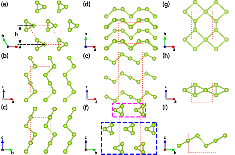
The -phase crystalline structure of bulk selenium and tellurium is schematically shown in Figs. 1(a), 1(b) and 1(c). It consists of parallel-aligned helical chains arranged in a hexagonal array Teuchert1975 ; Keller1977 . Every atom is covalently bonded to two neighboring atoms along each chain, and interacts weakly with atoms on the adjacent chains. Figure 1(a) shows that bulk selenium and tellurium may be viewed as a layered structure. Different layers are stacked in the direction perpendicular to (or ) planes and each layer consists of one-dimensional array of single helical chains stretched to infinity along the -axis. An layer 2D structure is made of helical chain layers stacked in the bulk mode [see Figs. 1(d), 1(e) and 1(f)]. Interestingly, the space group of an odd-number layer structure is (), while that of an even-number layer structure is () (see Table II). Note that -phase bulk and few-layer structures all possess broken inversion symmetry, the necessary condition for nonzero second-order NLO responses. However, the -phase ML tellurium is unstable against the -phase, a structure with centrosymmetry [see Figs. 1(g), 1(h) and 1(i)]. Nonetheless, for all other atomically thin Te films, -phase is the most stable structure. Also, for all the atomically thin Se films, -phase is the most stable structure. Therefore, we consider only bilayer (BL) and trilayer (TL) tellurium as well as ML, BL and TL selenium. In the present calculations, 2D selenium and tellurium structures are modeled by using the slab-superlattice approach. The separations between the 2D structures adopted are about 20 Å, to ensure negligible interaction between the periodic images.
| SCAN | optB88-vdW | PBE-D2 | PBE | exp | ||
|---|---|---|---|---|---|---|
| Se | 4.4336 | 4.2348 | 4.2517 | 4.4984 | 4.366211footnotemark: 1 | |
| 4.9984 | 5.1319 | 5.1065 | 5.0526 | 4.953611footnotemark: 1 | ||
| Te | 4.4578 | 4.4816 | 4.3357 | 4.5085 | 4.451122footnotemark: 2 | |
| 5.9291 | 5.9951 | 6.0300 | 5.9593 | 5.926222footnotemark: 2 |
Experimental value from reference Teuchert1975, .
Experimental value from reference Keller1977, .
| bulk Se | ML Se | BL Se | TL Se | bulk Te | BL Te | TL Te | |
|---|---|---|---|---|---|---|---|
| space group | 21 | 2 | 2 | 21 | 2 | ||
| (Å) | 4.434 | 4.918 | 4.955 | 4.968 | 4.458 | 5.791 | 5.839 |
| (Å) | 4.434 | 4.198 | 4.287 | 4.336 | 4.458 | 4.311 | 4.367 |
| (Å) | 4.998 | 5.929 | |||||
| (Å) | 3.781 | 7.562 | 11.344 | 7.71 | 11.564 | ||
| (Å) | 3.50 | 3.34 | 3.55 | 3.54 | 3.47 | 3.51 | 3.48 |
| (Å) | 2.38 | 2.36 | 2.37 | 2.37 | 3.17 | 2.85 | 2.84 |
| 1.47 | 1.42 | 1.50 | 1.49 | 1.09 | 1.23 | 1.23 |
Our density functional theory calculations are performed by using the highly accurate projector augmented wave (PAW) method blochl1994 , as implemented in the VASP package kresse1996ab ; kresse1996 . A large plane-wave cutoff energy of 450 eV is used throughout. The PAW potentials for Se and for Te are adopted to describe the electron-ion interaction. The theoretical atomic positions and lattice constants are obtained when the forces acting on all the atoms are less than 0.001 eV/Å and the stresses are less 1.0 kBar. The total energy convergence criterion for the self-consistent electronic structure calculations is eV. The accurate tetrahedron method blochl1994tetrahedron is used for the Brillouin zone integration. The self-consistent charge density calculations are performed with -point meshes of 18201 for 2D Se and 15201 for multilayer Te.
To obtain accurate structure parameters, we first perform structural optimizations for bulk selenium and tellurium with the conjugate gradient technique using the SCAN Sun2015 ; Peng2016 , optB88-vdW Thonhauser2007 , Perdew-Burke-Ernzerhof (PBE) perdew1996 , DFT-D2 Grimme2006 exchange-correlation functionals. The calculated lattice constants are listed in Table I. The lattice constants calculated using the SCAN functional are in the best agreement with experiments Teuchert1975 ; Keller1977 (see Table I). Therefore, in all the geometric optimization calculations for the 2D structures, we adopt the SCAN functional.
Using the structural parameters for the 2D structures determined by using the SCAN functional, we first perform the self-consistent band structure calculations within the generalized gradient approximation (GGA) of the PBE functional perdew1996 . We then calculate the optical dielectric function and NLO responses of the 2D structures from the calculated band structures within the linear response formalism with the independent-particle approximation. In particular, the imaginary part of the dielectric function due to direct interband transition in the atomic units is given by (see, e.g., Refs. guo2004 ; Guo2005ab ),
| (1) |
where is the unit-cell volume, is the weight for the point and is the photon energy. VB and CB stand for the valence and conduction bands, respectively. The dipole transition matrix elements , where represents Cartesian component of the dipole operator, are obtained from the band structures within the PAW formalism Adolph2001 . Here k is the th Bloch state function with momentum k. The real part of the dielectric function is then obtained from the calculated by the Kramer-Kronig transformation guo2004 ; Guo2005ab ,
| (2) |
where denotes the principal value of the integral.
The imaginary part of the second-order NLO susceptibility due to direct interband transitions is given by guo2004 ; guo2005
| (3) |
where the contribution due to the so-called virtual-electron (VE) process is guo2004 ; guo2005
| (4) |
and that due to the virtual-hole (VH) process is guo2004 ; guo2005
| (5) |
Here = - and . The real part of the second-order NLO susceptibility is obtained from the calculated by the Kramer-Kronig transformation guo2004 ; guo2005
| (6) |
The LEO coefficient is related to the second-order NLO susceptibility Hughes1996 ; Prussel2018 . In the zero frequency limit Hughes1996 ; Prussel2018 ,
| (7) |
In the very low frequency region, i.e. the photon energy well below the band gap, and are nearly constant. In this case, the LEO coefficient wang2015 ; guo2004 .
The DC shift current along the -axis is given by
| (8) |
where is the third-rank conductivity tensor. Sipe2000 Within the length gauge formalism, can be written in terms of the interband position matrix element and its momentum derivative (see Eq. (57) in Ref. Sipe2000 ). By replacing with , one would obtain
| (9) |
In the present calculations, the function in Eqs. (1), (4), (5) and (9) is approximated by a Gaussian function with eV. The point weight is set to where is the total number of the sampled -points. To obtain accurate optical properties, we perform calculations for selenium and tellurium with several different -point meshes until the calculated optical properties converge to a few percent. Therefore, adequately dense -point meshes of 52601 and 45601 are adopted for selenium and tellurium, respectively. Furthermore, 30 energy bands per atom are included in the present optical calculations in order to ensure that and obtained by the Kramer-Kronig transformation are reliable. In the slab-supercell approach, the unit cell volume in Eqs. (1), (4), (5) and (9) is not well-defined for 2D Se and Te. In the literature, two ways have been adopted to resolve this problem. Gruning2014 ; Trolle2014 ; wang2015 ; Attaccalite2015 ; hu2017 ; wang2017 ; panday2018 ; Attaccalite2019 ; Rangel2017 One way is to present the 2D response functions in terms of per unit width simply by multiplying the calculated quantities with the supercell lattice constant along the perpendicular direction Trolle2014 ; wang2017 . Physically, this means the optical responses coming from a single atomically thin film Trolle2014 ; wang2017 . The other way is to use the effective unit cell volume Gruning2014 ; wang2015 ; Attaccalite2015 ; hu2017 ; panday2018 ; Attaccalite2019 ; Rangel2017 , which is given by the area of the in-plane unit cell times the effective thickness (see Table II). This quasi bulk approach would allow one to compare the calculated quantities with that of bulk materials, and thus is adopted in this paper. Nevertheless, one should keep in mind that to evaluate the total responses from a single film, one should multiply the quantities by the effective thickness rather than light penetration depth.
III Electronic band structure
| (eV) | (eV) | (eV) | (eV) | ||
|---|---|---|---|---|---|
| Se | ML | 1.857 | 2.600 | 0.756 | |
| BL | 1.503 | 2.270 | 0.744 | ||
| TL | 1.305 | 2.078 | 0.743 | ||
| bulk | 1.00211footnotemark: 1 | 1.73511footnotemark: 1 | 2.022footnotemark: 2 | ||
| Te | BL | 0.864 | 1.128 (1.1733footnotemark: 3) | 0.8544footnotemark: 4 | 0.289 |
| TL | 0.654 | 1.072 (0.9533footnotemark: 3) | 0.7444footnotemark: 4 | 0.299 | |
| bulk | 0.11311footnotemark: 1 | 0.32211footnotemark: 1 | 0.32355footnotemark: 5 |
Theoretical value from reference Cheng2019, .
Experimental value from reference Tutihasi1967, .
Theoretical value from reference qiao2018, .
Experimental value from reference Huang2017, .
Experimental value from reference Anzin1977, .
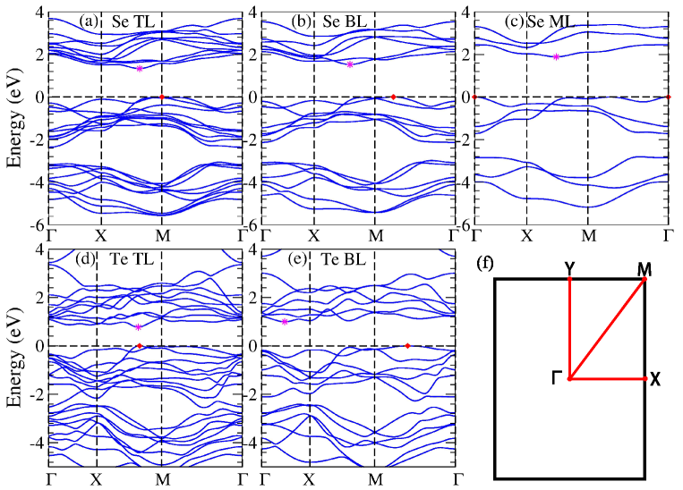
To understand the electronic and optical properties of 2D Se and Te materials, we plot their electronic band structures in Fig. 2. Clearly, Fig. 2 shows that all the 2D Se and BL Te are indirect band gap semiconductors, while TL Te has a nearly direct band gap. For BL tellurium, the valence band maximum (VBM) is close to the M point along the M- direction, while the conduction band minimum (CBM) is located somewhere close to the along the -X symmetry line. If the thickness of ultrathin Te film increases to that of TL, both VBM and CBM are located at a general -point close to the M along the X-M direction, i.e., TL Te is a nearly direct band gap semiconductor and thus may have promising applications in semiconductor devices. In contrast, a band gap transition from the direct to indirect one occurs as the thickness for the 2D MoS2 film increases from ML to bulk. Chei2012 Interestingly, when the thickness of 2D selenium increases from ML to TL, the location of the VBM moves from symmetry point to M along the -M line. The CBM is located at a general -point along the X-M symmetry line. Nevertheless, it gets closer to the M point with the thickness [see Figs. 2(a), (b) and (c)]. Clearly, the band gap of 2D selenium is larger than that of the corresponding 2D tellurium (see Table III) due to the increased ionization energy. In general, the band gaps of 2D Se and Te materials are tunable by varying the number of layers.
It is well known that the band gap of a semiconductor is generally underestimated by the GGA calculations (see, e.g., Table III). Therefore, to obtain more accurate band gaps, we also calculate the band structures by using the hybrid Heyd-Scuseria-Ernzerhof (HSE) functional heyd2003 , which is known to produce much improved band gaps for semiconductors. The theoretical band gaps from the HSE and GGA calculations together with the experimental values are listed in Table III. The band structures from the HSE calculations with the spin-orbit coupling (SOC) included are displayed in Fig. S1. Indeed, Table III shows that the band gaps of bulk selenium and tellurium from the HSE-SOC calculations Cheng2019 agree rather well with the corresponding experimental values. Therefore, we use the band gaps from the HSE-SOC calculations and the scissors correction scheme levine_prb_1991 to evaluate linear and NLO properties for 2D Se and Te considered here. We notice that the band gap from the HSE-SOC calculation is 1.128 (1.072) eV in BL (TL) tellurium, which agrees rather well with that reported in Ref. qiao2018 (see Table III). The small difference stems from the fact that the band gaps from Ref. qiao2018 are based on the optB88-vdW structure, while we use the structures from the SCAN structural optimizations. It is worthwhile to point out that the gap of BL Te from the HSE-SOC calculations is close to 1.3 eV, the ideal gap value for perfect solar energy absorption efficiency Cai2017 . Therefore, one could expect BL Te to have high solar energy absorption efficency, thereby leading to high power conversion efficiency for photovoltaic devices.
We notice that the experimental band gaps for BL and TL tellurium are smaller than that from our HSE-SOC calculations. This discrepancy is likely due to the effect of the graphene substrate because the environment can significantly affect the electronic properties of 2D materials Huser2013 ; Ugeda2014 ; Rasmussen2015 . The graphene substrate can reduce the band gap of BL and TL tellurium mainly in two ways, namely, via (1) changing the structural parameters due to lattice mismatch and (2) offering extra dielectric screening. In particular, the in-plane lattice constants for atomically thin Te films on graphene substrate were reported Huang2017 to be Å and A, which are 2.3 % and 3.3 % larger than that of BL Te (see Table II), respectively. It was reported Rasmussen2015 that the band gap of MoS2 ML would get reduced by as much as 0.46 eV upon a lattice expansion of 2 %. Our GGA calculation for BL Te using the reported lattice constants Huang2017 results in a band gap reduction of 0.1 eV. The substrates have also been found to introduce significant extra screening, thus reducing the band gap (see, e.g., Refs. Huser2013 ; Ugeda2014 ). For example, putting a BN sheet on graphene would reduce the band gap of BN ML by 1.02 eV (14 %) Huser2013 . Nonetheless, further investigations into the reduction of the band gaps of 2D tellurium due to substrates are beyond the scope of this paper.
IV Linear optical property
In Fig. 3 and Fig. 4, the calculated real and imaginary parts of the optical dielectric function of 2D selenium and tellurium are shown, respectively. Bulk Se and Te have a trigonal lattice with the helical chains along the -axis [see Figs. 1(a), 1(b) and 1(c)] and thus exhibit a rather strong uniaxial optical anisotropy Cheng2019 because of the weak inter-chain interaction. In contrast, 2D Se and Te form a 2D rectangular lattice with the helical chains lying along the -axis (see Fig. 1), and this may result in a strong in-plane optical anisotropy. Consequently, the real and imaginary parts of the dielectric function of 2D Se and Te compose of three independent components, namely, light polarization parallel () and perpendicular ( and ) to the axis.
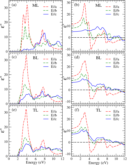
Figure 3 shows that overall, the dielectric functions of ML, BL and TL selenium look rather similar due to the weak interlayer interaction. For example, there is a very prominant peak near 4.0 eV in the spectrum of for all three multilayers. Also, in the low-energy region of about 2.5-5.5 eV, the optical anisotropy is strong in all three multilayers. In the high-energy region of about 5.5-10 eV, there is a prominent peak and two shoulders for for all three structures. For and , the amplitude of the peaks gradually decreases with the film thickness. There are also some differences. For example, Fig. 3(a) shows that in ML Se, there is a rather sharp peak near 3.3 eV for and also near 8.0 eV for which, however, appears as a weak shoulder and bulge, respectively, in the spectra of BL Se [Fig. 3(c)] and TL Se [Fig. 3(e)]. This difference may be caused by a stronger quantum confinement in ML selenium. Furthermore, Fig. 3(a) indicates that optical absorption for in 2.5-5.5 eV is very weak. Nevertheless, the absorption increases significantly with the film thickness [Fig. 3(c) and Fig. 3(e)]. Additionally, these peaks become oscillatory bulges in the structures, particularly in TL selenium. This could be explained by the fact that the interlayer interaction is weak but not negligible. In particular, the real and imaginary parts of the optical dielectric function for BL and TL selenium are rather similar except the spectrum. The same phenomenon has been observed in Cr2Ge2Te6 fang2018 . It is noted that the optical spectra for (parallel to the chain direction) and for (perpendicular to the layers) of TL selenium are nearly identical to the corresponding spectra of bulk selenium Cheng2019 . In other words, the optical properties of TL selenium are like that of quasi-1D systems.
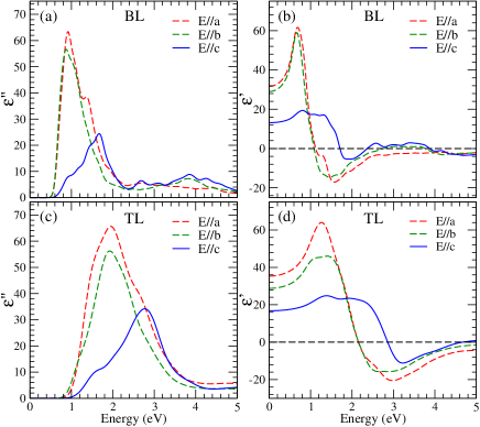
As for 2D selenium, Fig. 4 indicates that overall, the dielectric functions of BL and TL tellurium are quite similar due to the weak interlayer interaction. In particular, there is a very prominant peak near 2.0 eV in the spectra of and for both multilayers. Furthermore, the optical spectra of and for both multilayers are very similar, indicating almost no in-plane optical anisotropy. This is in contrast to 2D selenium in which the peak height for is much smaller than that of , indicating a strong in-plane optical anisotropy there. This could be explained by the fact that the relative in-plane inter-chain distance () in 2D selenium is much larger than in 2D tellurium (see Table II). On the other hand, Te 5 orbitals are much larger than Se 4 orbitals, as indicated by the intrachain atomic distance () (see Table II). Consequently, these result in a much stronger in-plane interchain bonding in 2D tellurium and hence a much weaker in-plane optical anisotropy. For , this peak shifts to 3.4 eV and 2.8 eV for BL and TL tellurium [see Figs. 4(a) and 4(c)], respectively. Also, in the low-energy region up to 3.0 eV, the optical spectra for in-plane and perpendicur polarizations differ significantly in both multilayers. Above 3.0 eV, the optical spectra for all three polarizations look rather similar.
V Second harmonic generation and linear electro-optic effect
Bulk selenium and tellurium have five nonzero SHG susceptibility elements since their symmetry is either (right-handed screw) or (left-handed screw). Cheng2019 However, 2D selenium and tellurium possess a lower symmetry and thus have more nonzero SHG susceptibility elements. As mentioned above, their space group depends on the number of layers (), namely, () for the odd and () for the even . Nonetheless, the two space groups have the same nonzero elements. Therefore, all 2D selenium and tellurium materials considered here have eight nonzero SHG elements as , , , , , , and .
| bulk | 9.011footnotemark: 1 | 12.711footnotemark: 1 | 14511footnotemark: 1 | 511footnotemark: 1 | -3.5811footnotemark: 1 | -0.1211footnotemark: 1 | |||||||||||||
| ML | 11.5 | 8.2 | 5.1 | 41 | 155 | 3 | 36 | 40 | 28 | 4 | 32 | -0.63 | -3.29 | -0.10 | -0.77 | -1.92 | -0.60 | -0.29 | -1.08 |
| BL | 11.9 | 8.2 | 6.4 | 17 | 92 | -6 | 27 | 27 | 12 | -11 | 25 | -0.24 | -1.87 | 0.15 | -0.54 | -1.01 | -0.24 | 0.52 | -0.65 |
| TL | 12.0 | 8.3 | 7.0 | 12 | 75 | -11 | 18 | 19 | 1 | -16 | 16 | -0.17 | -1.51 | 0.25 | -0.37 | -0.65 | -0.03 | 0.64 | -0.37 |
Calculated value from reference Cheng2019, .
V.1 2D selenium
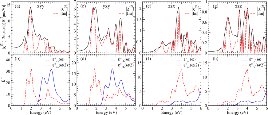
The real and imaginary parts of the SHG coefficients for ML selenium are displayed in Fig. 5, while that of BL and TL selenium are shown, respectively, in Fig. S2 and Fig. S3 in the Supplementary Material (SM). SM As for the linear optical property case, the calculated SHG coefficients for all the 2D Se structures are rather similar (see Figs. 5, S2 and S3) due to the weak interlayer interaction. For example, they all show that the spectra have the largest magnitude among the nonzero SHG matrix elements in the entire optical frequency range, and their spectra are similar to the spectra of bulk selenium Cheng2019 . They all have a prominent peak at 1.98 eV in the spectrum. Nonetheless, this peak height get reduced from ML Se (1420 pm/V) to BL Se (1020 pm/V) and to TL Se (840 pm/V). The absolute value of SHG element of ML selenium at 1.98 eV is 1423 pm/V, which is nearly 2 times larger than that of bulk selenium, and is also 6 times larger than that of GaN Gavrilenko2000 ; Cai2009 , a widely used NLO semiconductor. Figures 5, S2 and S3 indicate that all the nonzero SHG elements of all the 2D Se structures are rather large and purely dispersive for photon energy less than half of the band gap (). For example, of ML selenium (see Table IV) is nearly 20 times larger than of GaN Gavrilenko2000 ; Cai2009 . This suggests that 2D selenium may have potential applications in low-loss NLO optical devices.
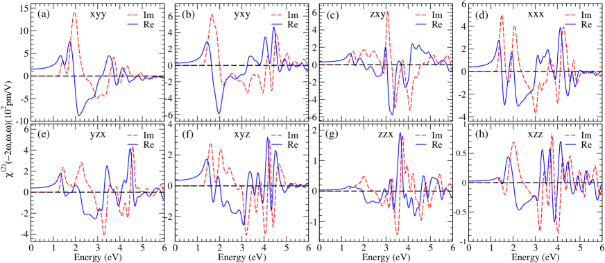
In what follows, we take ML selenium as an example to perform a detailed analysis. In order to further analyze the prominent features in the calculated spectra of ML selenium, we plot the absolute values of the imaginary part of and compare them with the absorptive part of the dielectric function in Fig. 6. Because they have similar features, only four elements out of the eight nonzero SHG elements are presented in Fig. 6. The SHG involves not only single-photon resonance but also double-photon resonance. Figure 6(a) shows that the spectrum can be divided into two parts. The first part from 1.22 to 2.40 eV is primarily derived from double-photon resonances. On the other hand, the second part (above 2.40 eV) originates predominantly from single-photon resonances with some contribution from double-photon resonances [see Figs. 6(a) and (b)]. In this energy region, the spectra oscillate rapidly and also decrease gradually with photon energy due to the mixing of one- and two-photon resonances. Notably, for the spectrum, the first prominent peak at 1.70 eV corresponds to the pronounced peak in the [see Figs. 6(c) and 6(d)], suggesting that it stems from two-photon resonances. It is clear from Fig. 6(d) that the peaks above the absorption edge of are related to the and spectra, indicating that they can be caused by both double- and single-photon resonances. Figures 6(e) and 6(g) show that the peaks in and from the absorption edge of to the absorption edge of may be attributed to the two-photon resonances with Ec [cf. ]. Above the absorption edge of , the absolute values of the imaginary part of oscillate rapidly. This is consistent with the fact that in this energy region comes mainly from two-photon resonances with some contribution from one-photon resonances. Clearly, the modulus of the imaginary part of is larger than that of , and is also much larger than that of and . Interestingly, this can be correlated with the magnitude relationship of , and [or , and .
The calculated static SHG susceptibility and LEO coefficient as well as dielectric constant of bulk and 2D selenium are presented in Table IV. As for the optical frequency case discussed above, the static SHG susceptibility of 2D selenium is also highly anisotropic. In particular, of ML selenium is over 50 times larger than (see Table IV). Nevertheless, Table IV indicates that the anisotropy in the LEO coefficient gets much reduced because of the strong anisotropy of the static [See Eq. (7)]. Remarkably, LEO coefficient ( 3.29 pm/V) of ML Se is nearly 6 times larger than that of bulk GaN polytypes Gavrilenko2000 ; Cai2009 , suggesting that 2D selenium may become promising electric-optic materials for opto-electronic devices.
| bulk | 33.211footnotemark: 1 | 49.011footnotemark: 1 | 16911footnotemark: 1 | 100911footnotemark: 1 | -0.3011footnotemark: 1 | -1.8211footnotemark: 1 | |||||||||||||
| BL | 31.6 | 29.0 | 13.2 | 557 | 1077 | 31 | 592 | 585 | 897 | 0 | 591 | -1.11 | -2.34 | -0.15 | -1.29 | -3.06 | -1.95 | 0 | -2.84 |
| TL | 35.3 | 28.8 | 16.8 | 823 | 872 | 18 | 656 | 644 | 683 | -11 | 626 | -1.32 | -1.72 | -0.06 | -1.29 | -2.67 | -1.34 | 0.08 | -2.11 |
Calculated value from reference Cheng2019, .
V.2 2D tellurium
The calculated static dielectric constant , SHG susceptibility and LEO coefficient of 2D and bulk tellurium are listed in Table V. First of all, we notice that 2D Te exhibit much stronger static SHG responses than 2D Se. In particular, for BL Te (Table V) is more than 100 times larger than that of GaN in both zinc-blende and wurtzite structures Gavrilenko2000 ; Cai2009 . Thus, our calculations indicate that 2D Te may have valuable NLO applications such as frequency doublers. Nevertheless, as for 2D selenium, LEO coefficient () of BL Te is only 5 times greater than that of GaN Gavrilenko2000 ; Cai2009 , because static dielectric constant of BL Te also becomes larger than BL Se [see Tables IV and V as well as Eq. (7)].
The calculated real and imaginary parts of the SHG susceptibility of TL and BL tellurium are displayed, respectively, in Fig. 7 and Fig. S4 in the SM SM . Like 2D selenium, the spectral shape of the real and imaginary parts of for BL and TL tellurium are rather similar, indicating a weak interlayer interaction. Nevertheless, unlike 2D selenium, the spectrum has the largest magnitude in 2D tellurium (see Fig. 7). Furthermore, when one moves from BL tellurium (Fig. S4) to TL tellurium (Fig. 7), the magnitude of the spectrum increases significantly rather than decreases. Another striking difference is that the spectra of 2D tellurium in general are more than 10 times larger than the corresponding spectra in 2D selenium (see, e.g., Figs. 7 and S3). In particular, the peak height near 1.2 eV in the spectrum of TL selenium [Fig. S3(g)] more than 40 times smaller than that of TL tellurium [Fig. 7(a)]. For a specific semiconductor, the smaller the band gap is, the larger the magnitude of the second-order NLO susceptibility, as can be seen from Eqs. (4) and (5). This is the main reason why 2D tellurium generally have much larger SHG coefficients than 2D selenium (see also Tables IV and V) because of the much smaller band gaps of 2D tellurium.
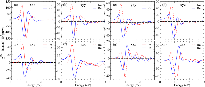
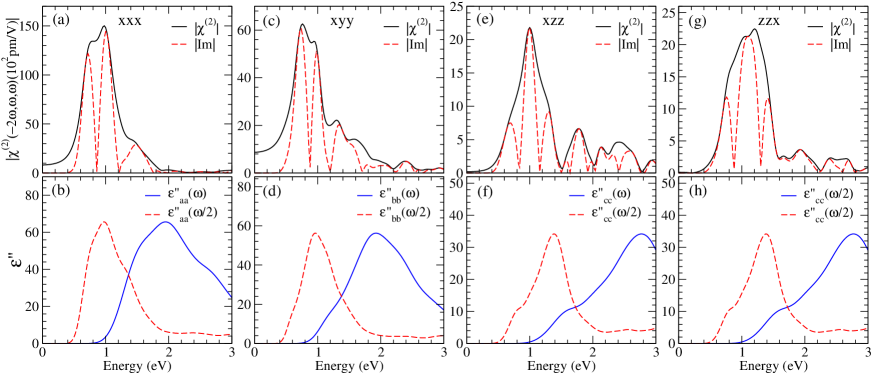
Let us now focus on the spectrum since it is the largest nonzero element among all the nonvanishing SHG coefficients of 2D tellurium. Figure 7(a) shows that is large in the photon energy range from 0.0 eV to 1.86 eV. In the energy range from 0.0 to 0.22 eV, the real part of the remains almost constant. As photon energy further increases, it increases steadily, and produces a small peak at 0.58 eV [see Fig. 7(a)]. In the energy region of 0.70-1.02 eV, the spectrum of becomes negative and forms a huge negative peak at 0.86 eV. Beyond 1.02 eV, it becomes positive again and decreases gradually in the higher energy region. The imaginary part of forms a sine-function shape in the photon energy range from 0.5 to 1.7 eV with a large maximum of 12000 pm/V at 0.7 eV and a large minimum of pm/V at 1.0 eV [see Fig. 7(a)]. It is negligible outside this photon energy range. Interestingly, all the nonzero SHG coefficients of TL tellurium have nearly identical shapes (see Fig. 7). Finally, we note that the magnitude of at 0.98 eV is as high as 15000 pm/V, which is 4 times larger than that of bulk Te Cheng2019 and 65 times larger than that of GaN Gavrilenko2000 ; Cai2009 . All these suggest that few-layer tellurium would find promising applications in, e.g., optical switching, ultrathin second-harmonic and sum frequency generation devices, optical modulation, and light signal modulators.
In order to further understand the features in the calculated SHG spectra, the absolute values of the imaginary parts of four prominent elements , , and of TL tellurium are plotted in Fig. 8 as examples, together with the imaginary part of the dielectric function. Figure 8 suggests that the spectral feature of both and between 0.44 and 1.72 eV could be attributed to the two-photon resonances shown in . In contrast, the structure above 1.72 eV stems from both single-photon [see ] and two-photon resonances [see ]. As a result, the SHG spectra, especially , oscillate rapidly and diminish gradually in the higher energy range [see Figs. 8(e) and 8(g)]. Similarly, for and , the spectral structures between 0.34 eV and 1.36 eV are mainly due to double-photon () resonances for and [see and ], respectively. The features in and for photon energies above 1.36 eV could be attributed to the single-photon resonances as can be seen from and , respectively. Clearly, the magnitude of is largest, and also is about several times larger than the other nonzero elements (see Fig. 7). Interestingly, this seems to be correlated with the fact that the magnitude of [] is larger than that of [], and much larger than [ ].
VI Bulk Photovoltaic Effect
The generation of photocurrents is a crucial component for solar energy harvesting. A promising mechanism for the photocurrent generation is the BPVE in which DC currents are generated in a noncentrosymmetric material under light irradiation. Young et al. recently demonstrated that the shift current dominates the BPVE in BaTiO3 Young2012 . In this section, we present the calculated nonzero elements of the shift current conductivity tensor for all the 2D selenium and tellurium considered here.
We notice that nonzero elements of the shift current conductivity tensor are the same as that of the SHG susceptibility tensor. Therefore, for all the 2D selenium and tellurium considered here, the nonzero elements are , , , , , , and . However, since we consider only the shift current generation due to the linearly polarized light here, we will present only the calculated shift current elements of , and in this paper. Furthermore, here we have also calculated the shift current conductivity tensors for bulk selenium and bulk tellurium for comparison. The computational details were already reported in Ref. Cheng2019 . Their space group is and there are two independent shift current elements among the five nonzero elements, i.e., and . The calculated two independent shift current elements of bulk selenium and bulk tellurium are displayed in Fig. 9.

VI.1 2D selenium
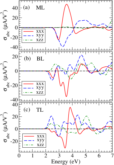
The calculated shift current spectra of 2D selenium are plotted in Fig. 10. It is clear that unlike the dielectric function and SHG spectra, the shift current spectra exhibit a strong layer-thickness dependence. Furthermore, the spectrum in general has the largest magnitude and the has the smallest magnetiude. In particular, the spectrum of ML selenium is negligibly small compared with the and spectra [see Fig. 10(a)]. This is clearly due to the very small absorption of light polarized along the layer normal direction in this photon energy range [see Fig. 3(a)]. As the layer thickness increases when one moves from ML selenium to BL and TL selenium, the optical absorption of the out-of-plane polarized light increases (see Fig. 3) and hence the magnitude of the spectrum also increases (see Fig. 10). Interestingly, the height (47 A/V2) of the maximal peak of the spectrum at 3.58 eV of ML selenium is larger than that of the spectrum at 3.56 eV (-36 A/V2) for BL selenium and also at 3.84 eV (35 A/V2) for TL selenium. We notice that the magnitudes of the spectra of 2D selenium are at least comparable to that of the and spectra of BaTiO3 Young2012 , an archetypical ferroelectric BPVE material. These magnitudes are also comparable to that of ML group-IV monochalcogenides (e.g., GeS) Rangel2017 . Therefore, 2D selenium may become excellent materials for photovoltaic solar cells. Figures 9(a) and 10 indicate that the shift current conductivities of bulk and 2D selenium are in the same order of magnitude, although their spectral shapes are quite different.
VI.2 2D tellurium
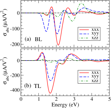
We display the calculated shift current conductivity () spectra of BL and TL tellurium in Fig. 11. First of all, we notice that the spectra of 2D tellurium are large in the optical frequency range, being nearly one-order of magnitude larger than the corresponding spectra of 2D selenium (see Fig. 10). This notable difference between 2D tellurium and 2D selenium may be attributed to the smaller band gaps and highly covalent bonding in 2D tellurium. Furthermore, the magnitude of the at 1.66 eV of TL tellurium is nearly 4 times larger than the maximum of the shift current conductivities of ML GeS Rangel2017 . In fact, the shift current conductivity of ML Ge and Sn monochalcogenides apparently is larger than that of other noncentrosymmetric semiconductors reported so far Rangel2017 . This indicates that 2D tellurium are very promising materials for photovoltaic devices. The spectrum in general has the largest magnitude while the has the smallest magnetiude. Indeed, the spectrum of TL tellurium is negligibly small compared with the and spectra [see Fig. 11(b)]. Second, unlike the dielectric function and SHG spectra, the shift current spectra exhibit a strong layer-thickness dependence. In particular, the height of the prominent negative peak at 1.7 eV in the spectrum of TL tellurium is nearly twice as large as that of the negative peak at 2.1 eV in BL tellurium (see Fig. 11). In contrast to 2D selenium, 2D tellurium have the shift current conductivities that are much larger than bulk tellurium (see Figs. 9(b) and 11). In particular, the shift current conductivities of TL Te [Fig. 11(b)] are as much as five times larger than that of bulk tellurium [Fig. 9(b)]. Our work thus demonstrates that few-layer tellurium with narrow band gaps are promising materials for high efficient photovoltaic solar cells.
VII Discussion
For a specific semiconductor, low frequency NLO properties depend significantly on its band gap. This could be seen from the fact that the energy differences between the initial and final states of the optical transitions are in the denominators of Eqs. (4), (5) and (9). This indicates that the smaller the band gap is, the larger the magnitude of the NLO responses would be. For example, for the imaginary part of the SHG coefficients, the magnitude in the low frequency region would be roughly proportional to the inverse of the fourth power of the band gap [see Eqs. (4) and (5)]. Equation (9) also indicates that the magnitude of the shift current conductivity is roughly proportional to the inverse of the third power of the band gap. As a result, although 2D Se and Te have identical crystalline structures and similar band structures, the calculated imaginary part of the dielectric function, SHG coefficients and shift photoconductivities for 2D Te are much larger than that of 2D Se simply because 2D Te has a much smaller band gap. Interestingly, unlike bulk Te, few-layer Te have a band gap being larger than the optical frequencies of interest, showing that the materials would be useful for the NLO applications.
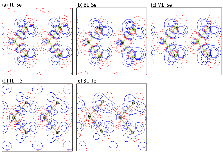
As mentioned in the preceding sections, compared to other semiconductors with similar band gaps, 2D Se and Te generally exhibit much larger NLO effects. To further understand the origins of the enhanced NLO responses of 2D selenium and tellurium, we calculate the difference charge density which is defined as the difference between the total charge density and the superposition of the free atomic charge densities, as displayed in Fig. 12. Figures 12(a), 12(b) and 12(c) [Figs. 12(d) and 12(e)] show that a considerable electron charge buildup occurs in the vicinity of the Se-Se (Te-Te) bond center by depleting the charge around the atoms along the bond directions in 2D selenium (2D tellurium). This indicates that there is strong directional covalent bonding in these 2D materials. It is known that strong covalent bonding would generate large spatial overlap between the wave functions of initial and final states and thus leads to large optical matrix elements, thereby resulting in enhanced NLO responses. Furthermore, Fig. 12 also shows a charge buildup around each atom in the direction perpendicular to the chain, indicating the existence of lone-pair electrons. The presence of lone-pair electrons is beneficial to the generation of induced dipole oscillations by the optical electric fields, thus leading to larger values Jiang2014 ; Cammarata2014 and other NLO effects. We notice that these features in the difference charge density distributions in 2D Se and Te are quite similar to that found in bulk trigonal Se and Te Cheng2019 . Bulk Se and Te crystalize in helical chainlike structures and also exhibit large SHG and LEO effect Cheng2019 . Therefore, in general, quasi one-dimensional crystals with strong directional covalency and lone-pair electrons would possess large NLO values. Moreover, high anisotropy would result in large joint DOS, and hence give rise to larger BPV and SHG effect Ingers1988 ; Song2009 .
Therefore, in general, to search for the materials with large NLO responses, one first should focus on those semiconductors with smallest possible band gaps which are larger than the optical frequencies required by specific NLO applications. Second, one should also pay attention to low dimensional systems with high anisotropy, strong covalency and/or lone-pair electrons.
VIII CONCLUSION
We have carried out a systematic first-principles investigation on the nonlinear optical properties of 2D selenium and tellurium within the generalized gradient approximation plus scissors correction. We find that all the 2D materials possess large NLO responses. In particular, TL Te exhibits a SHG coefficient of up to 15000 pm/V, which is 65 times larger than that of bulk GaN. BL Te exhibits gigantic static SHG coefficient , which is more than 100 times larger than that of bulk GaN. ML Se also displays prominent NLO effects with maximal nonvanishing SHG coefficient being as large as 1400 pm/V, which exceeds 6 times larger than that of GaN. Furthermore, ML Se and BL Te have large LEO coefficients and , being up to 6 times and 5 times larger than that of bulk GaN polytypes, respectively. We also find that the maximum of the shift current in the visible frequency range for TL Te is two times larger than that of ML GeS. All these findings suggest that 2D selenium and tellurium are promising NLO materials for applications in, e.g., photovoltaic devices, second-harmonic generation, sum frequency generation, frequency conversion, phase matching, electro-optical switches and light signal modulators. The features in the SHG spectra of the 2D Se and Te are correlated with the peaks in the imaginary part of the corresponding optical dielectric function in terms of single-photon and double-photon resonances. We believe that this work will stimulate further experiments on the second-order nonlinear optical responses of these fascinating elemental 2D materials.
ACKNOWLEDGEMENTS
M. C. thanks Department of Physics and Center for Theoretical Physics, National Taiwan University for its hospitality during her three months visit. Work at Xiamen University is supported by the National Key RD Program of China (Grant No. 2016YFA0202601), and the National Natural Science Foundation of China (No. 11574257). G. Y. G. acknowledges support from the Ministry of Science and Technology, the Academia Sinica, the National Center for Theoretical Sciences in Taiwan.
References
- (1) Y. R. Shen, The Principle of Nonlinear Optics (John Wiley and Sons Inc., New Jersey, 2003).
- (2) R. W. Boyd, Nonlinear Optics (Elsevier Science, Amsterdam,2003).
- (3) R. K. Chang, J. Ducuing, and N. Bloembergen, Dispersion of the Optical Nonlinearity in Semiconductoros, Phys. Rev. Lett. 15, 415 (1965).
- (4) H. Zhong, Z. H. Levine, D. C. Allan, and J. W. Wilkins, Band-theoretic calculation of the optical activity tensor of -quartz and trigonal Se, Phys. Rev. B 48, 1384 (1993).
- (5) J. L. P. Hughes and J. E. Sipe, Calculation of second-order optical response in semiconductors, Phys. Rev. B 53, 10751 (1996).
- (6) V. I. Gavrilenko and R. Q. Wu, Linear and nonlinear optical properties of group-III nitrides, Phys. Rev. B 61, 2632 (2000).
- (7) D. J. Cai and G.-Y. Guo, Tuning linear and nonlinear optical properties of wurtzite GaN by -axial stress, J. Phys. D: Appl. Phys. 42, 185107 (2009).
- (8) M. J. Cheng, S. Q. Wu, Z.-Z. Zhu, and G.-Y. Guo, Large second-harmonic generation and linear electro-optic effect in trigonal selenium and tellurium, Phys. Rev. B 100, 035202 (2019).
- (9) G. Y. Guo, K. C. Chu, D.-S. Wang, and C.-G. Duan, Linear and nonlinear optical properties of carbon nanotubes from first-principles calculations, Phys. Rev. B 69, 205416 (2004).
- (10) G. Y. Guo and J. C. Lin, Second-harmonic generation and linear electro-optical coefficients of BN nanotubes, Phys. Rev. B 72, 075416 (2005); Erratum: Second-harmonic generation and linear electro-optical coefficients of BN nanotubes [Phys. Rev. B 72, 075416 (2005)], 77, 049901 (2008).
- (11) M. Grüning and C. Attaccalite, Second harmonic generation in h-BN and MoS2 monolayers: Role of electron-hole interaction, Phys. Rev. B 89, 081102(R) (2014).
- (12) M. L. Trolle, G. Seifert and T. G. Pedersen, Theory of excitonic second-harmonic generation in monolayer MoS2, Phys. Rev. B 89, 235410 (2014).
- (13) C.-Y. Wang and G.-Y. Guo, Nonlinear optical properties of transition-metal dichalcogenide MX2 (M= Mo, W; X= S, Se) monolayers and trilayers from first-principles calculations, J. Phys. Chem. C 119,13268 (2015).
- (14) C. Attaccalite, A. Nguer, E. Cannuccia and M. Grüning, Strong second harmonic generation in SiC, ZnO and GaN two-dimensional hexagonal crystalls from first-principles many-body calculations, Phys. Chem. Chem. Phys. 17, 9533 (2015).
- (15) L. Hu, X. Huang, and D. Wei, Layer-independent and layer-dependent nonlinear optical properties of two-dimensional GaX (X= S, Se, Te) nanosheets. Phys. Chem. Chem. Phys. 19,11131 (2017).
- (16) H. Wang and X. F. Qian, Giant optical second harmonic generation in two-dimensional multiferroics. Nano Lett. 17, 5027 (2017).
- (17) S. R. Panday, and B. M. Fregoso, Strong second harmonic generation in two-dimensional ferroelectric IV-monochalcogenides, J. Phys.: Condens. Matter 29, 43LT01 (2017); Corrigendum: Strong second harmonic generation in two-dimensional ferroelectric IV-monochalcogenides (2017 J. Phys.: Condens. Matter 29 43LT01), 30, 179501 (2018).
- (18) C. Attaccalite, M. Palummo, E. Cannuccia and M. Grüning, Second-harmonic generation in single-layer monochalcogenides: A response from first-principles real-time similations, Phys. Rev. Mater. 3, 074003 (2019).
- (19) Q. Wu and X.-C. Zhang, Ultrafast electro-optic field sensors, Appl. Phys. Lett. 68, 1604 (1996).
- (20) A. G. Chynoweth, Surface Space-Charge Layers in Barium Titanate, Phys. Rev. 102, 705 (1956).
- (21) A. M. Glass, D. von der Linde, and T. J. Negran, High-voltage bulk photovoltaic effect and the photorefractive process in LiNbO3, Appl. Phys. Lett. 25, 233 (1974).
- (22) S. M. Young and A. M. Rappe, First Principles Calculation of the Shift Current Photovoltaic Effect in Ferroelectrics, Phys. Rev. Lett. 109, 116601 (2012).
- (23) A. Bhatnagar, A. R. Chaudhuri, Y. H. Kim, D. Hesse, and M. Alexe, Role of domain walls in the abnormal photovoltaic effect in BiFeO3, Nat. Commun. 4, 2835 (2013).
- (24) J. A. Brehm, S. M. Young, F. Zheng, and A. M. Rappe, First-principles calculation of the bulk photovoltaic effect in the polar compounds LiAsS2, LiAsSe2, and NaAsSe2, J. Chem. Phys. 141, 204704 (2014).
- (25) T. Rangel, B. M. Fregoso, B. S. Mendoza, T. Morimoto, J. E. Moore, and J. B. Neaton, Large Bulk Photovoltaic Effect and Spontaneous Polarization of Single-Layer Monochalcogenides, Phys. Rev. Lett. 119, 067402 (2017).
- (26) S.-J. Gong, F. Zheng, and A. M. Rappe, Phonon Influence on Bulk Photovoltaic Effect in the Ferroelectric Semiconductor GeTe, Phys. Rev. Lett. 121, 017402 (2018).
- (27) L. A. Agapito, N. Kioussis, W. A. Goddard III, and N. P. Ong, Novel Family of Chiral-Based Topological Insulators: Elemental Tellurium under Strain, Phys. Rev. Lett. 110, 176401 (2013).
- (28) H. Peng, N. Kioussis, and G. J. Snyder, Elemental tellurium as a chiral p-type thermoelectric material, Phys. Rev. B 89, 195206 (2014).
- (29) M. Hirayama, R. Okugawa, S. Ishibashi, S. Murakami, and T. Miyake, Weyl Node and Spin Texture in Trigonal Tellurium and Selenium, Phys. Rev. Lett. 114, 206401 (2015).
- (30) C. Şahin, J. Rou, J. Ma, and D. A. Pesin, Pancharatnam-Berry phase and kinetic magnetoelectric effect in trigonal tellurium, Phys. Rev. B 97, 205206 (2018).
- (31) S. S. Tsirkin, P. A. Puente, and I. Souza, Gyrotropic effects in trigonal tellurium studied from first principles. Phys. Rev. B 97, 035158 (2018).
- (32) H. O. H. Churchill, G. J. Salamo, S.-Q. Yu, T. Hironaka, X. Hu, J. Stacy, and I. Shih, Toward Single Atom Chains with Exfoliated Tellurium, Nanoscale Res. Lett. 12, 488 (2017).
- (33) I. L. Li, J. P. Zhai, P. Launois, S. C. Ruan, and Z. K. Tang, Geometry, Phase Stability, and Electronic Properties of Isolated Selenium Chains Incorporated in a Nanoporous Matrix, J. Am. Chem. Soc. 127, 16111 (2005).
- (34) D. J. Olechna and R. S. Knox, Energy-Band Structure of Selenium Chains, Phys. Rev. 140, A986 (1965).
- (35) M. Springborg, and R. O. Jones, Sulfur and selenium helices: Structure and electronic properties, J. Chem. Phys. 88, 2652 (1988).
- (36) P. Ghosh, M. U. Kahaly, and U. V. Waghmare, Atomic and electronic structures, elastic properties, and optical conductivity of bulk Te and Te nanowires: A first-principles study, Phys. Rev. B 75, 245437 (2007).
- (37) M. U. Kahaly, P. Ghosh, S. Narasimhan, and U. V. Waghmare, Size dependence of structural, electronic, elastic, and optical properties of selenium nanowires: A first-principles study, J. Chem. Phys. 128, 044718 (2008).
- (38) B. Tuttle, S. Alhassan, and S. Pantelides, Computational Predictions for Single Chain Chalcogenide-Based One-Dimensional Materials, Nanomaterials (Basel) 7, 115 (2017).
- (39) E. Andharia, T. P. Kaloni, G. J. Salamo, S.-Q. Yu, H. O. H. Churchill, and S. Barraza-Lopez, Exfoliation energy, quasiparticle band structure, and excitonic properties of selenium and tellurium atomic chains, Phys. Rev. B 98, 035420 (2018).
- (40) Y. Y. Pan, S. Y. Gao, L. Yang, and J. Lu, Dependence of excited-state properties of tellurium on dimensionality: From bulk to two dimensions to one dimensions, Phys. Rev. B 98, 085135 (2018).
- (41) J. K. Qin, G. Qiu, J. Jian, H. Zhou, L. M. Yang, A. Charnas, D. Y. Zemlyanov, C.-Y. Xu, X. F. Xu, W. Z. Wu, H. Y. Wang, and P. D. Ye, Controlled Growth of a Large-Size 2D Selenium Nanosheet and Its Electronic and Optoelectronic Applications, ACS Nano 11, 10222 (2017).
- (42) Z. L. Zhu, X. L. Cai, S. H. Yi, J. L. Chen, Y. W. Dai, C. Y. Niu, Z. X. Guo, M. H. Xie, F. Liu, J.-H. Cho, Y. Jia, and Z. Y. Zhang, Multivalency-Driven Formation of Te-Based Monolayer Materials : A Combined First-Principles and Experimental study, Phys. Rev. Lett. 119, 106101 (2017).
- (43) L. Xian, A. P. Paz, E. Bianco, P. M Ajayan, and A. Rubio, Square selenene and tellurene: novel group VI elemental 2D materials with nontrivial topological properties, 2D Mater. 4, 041003 (2017).
- (44) X.-X. Xue, Y.-X. Feng, L. Liao, Q.-J. Chen, D. Wang, L.-M. Tang, and K. Q. Chen, Strain tuning of electronic properties of various dimension elemental tellurium with broken screw symmetry, J. Phys.: Condens. Matter 30, 125001 (2018).
- (45) S. Sharma, N. Singh, and U. Schwingenschlögl, Two-Dimensional Tellurene as Excellent Thermoelectric Material, ACS Appl. Energy Mater. 1, 1950 (2018).
- (46) T. T. Debela and H. S. Kang, Phase polymorphism and electronic structures of TeSe2, J. Mater. Chem. C 6, 10218 (2018).
- (47) W. Zhang, Q. S. Wu, O. V. Yazyev, H. M. Weng, Z. X. Guo, W.-D. Cheng, and G.-L. Chai, Topological phase transitions driven by strain in monolayer tellurium, Phys. Rev. B 98, 115411 (2018).
- (48) Y. Chen, J. Y. Liu, J. B. Yu, Y. G. Guo, and Q. Sun, Symmetry-breaking induced large piezoelectricity in Janus tellurene materials, Phys. Chem. Chem. Phys. 21, 1207 (2019).
- (49) G. Liu, Z. B. Gao, and J. Ren, Anisotropic thermal expansion and thermodynamic properties of monolayer -Te, Phys. Rev. B 99, 195436 (2019).
- (50) J. L. Chen, Y. W. Dai, Y. Q. Ma, X. Q. Dai, W. K. Ho, and M. H. Xie, Ultrathin -tellurium layers grown on highly oriented pyrolytic graphite by molecular-beam epitaxy, Nanoscale 9, 15945 (2017).
- (51) Y. X. Wang, G. Qiu, R. X. Wang, S. Y. Huang, Q. X. Wang, Y. Y. Liu, Y. C. Du, W. A. Goddard III, M. J. Kim, X. F. Xu, P. D. Ye, and W. Z. Wu, Field-effect transistors made from solution-grown two-dimensional tellurene, Nat. Electron. 1, 228 (2018).
- (52) J. Peng, Y. Pan, Z. Yu, J. J. Wu, J. C. Wu, Y. Zhou, Y. Q. Guo, X. J. Wu, C. Z. Wu, and Y. Xie, Two-Dimensional Tellurium Nanosheets Exhibiting an Anomalous Switchable Photoresponse with Thickness Dependence, Angew. Chem. Int. Ed. 57, 13533 (2018).
- (53) A. Apte, E. Bianco, A. Krishnamoorthy, S. Yazdi, R. Rao, N. Glavin, H. Kumazoe, V. Varshney, A. Roy, F. Shimojo, E. Ringe, R. K Kalia, A. Nakano, C. S. Tiwary, P. Vashishta, V. Kochat, and P. M Ajayan, Polytypism in ultrathin tellurium, 2D Mater. 6, 015013 (2019).
- (54) S. D. Kang, T. Dai, S. Dang, X. Y. Ma, G. L. Wang, H. W. Li, P. Hu, F. M. Yu, X. Zhou, S. X. Wu, S. W. Li, Broadband photoresponse of tellurium nanorods grown by molecular beam epitaxy, Chem. Phys. Lett. 729, 49 (2019).
- (55) S. Deckoff-Jones, Y. X. Wang, H. T. Lin, W. Z. Wu, and J. J. Hu, Tellurene: A Multifunctional Material for Midinfrared Optoelectronics, ACS Photonics 6, 1632 (2019).
- (56) X. C. Huang, J. Q. Guan, Z. J. Lin, B. Liu, S. Y. Xing, W. H. Wang, and J. D. Guo, Epitaxial Growth and Band Structure of Te Film on Graphene, Nano Lett. 17, 4619 (2017).
- (57) J. S. Qiao, Y. H. Pan, F. Yang, C. Wang, Y. Chai, and W. Ji, Few-layer tellurium: one-dimensional-like layered elementary semiconductor with striking physical properties, Sci. Bull. 63, 159 (2018).
- (58) Y. Wang, C. C. Xiao, M. G. Chen, C. Q. Hua, J. D. Zou, C. Wu, J. Z. Jiang, S. Y. A. Yang, Y. H. Lu, and W. Ji, Two-dimensional ferroelectricity and switchable spin-textures in ultra-thin elemental Te multilayers, Mater. Horiz., 5, 521, (2018).
- (59) C. Wang, X. Y. Zhou, J. S. Qiao, L. W. Zhou, X. H. Kong, Y. H. Pan, Z. H. Cheng, Y. Chai, and W. Ji, Charge-governed phase manipulation of few-layer tellurium, Nanoscale, 10, 22263, (2018).
- (60) W. D. Teuchert, R. Geick, G. Landwehr, H. Wendel, and W.Weber, Lattice dynamics of trigonal selenium. I. Phonon spectra, J. Phys. C: Solid State Phys. 8, 3725 (1975).
- (61) R. Keller, W. B. Holzapfel, and H. Schulz, Effect of pressure on the atom positions in Se and Te, Phys. Rev. B 16, 4404 (1977).
- (62) P. E. Blöchl, Projector augmented-wave method, Phys. Rev. B 50, 17953 (1994).
- (63) G. Kresse and J. Furthmüller, Efficient iterative schemes for ab initio total-energy calculations using a plane-wave basis set, Phys. Rev. B 54, 11169 (1996).
- (64) G. Kresse and J. Furthmüller, Efficiency of ab-initio total energy calculations for metals and semiconductors using a plane-wave basis set, Comput. Mater. Sci. 6, 15 (1996).
- (65) P. E. Blöchl, O. Jepsen, and O. K. Andersen, Improved tetrahedron method for Brillouin-zone integrations, Phys. Rev. B 49, 16223 (1994).
- (66) J. W. Sun, A. Ruzsinszky, and J. P. Perdew, Strongly Constrained and Appropriately Normed Semilocal Density Functional, Phys. Rev. Lett. 115, 036402 (2015).
- (67) H. W. Peng, Z.-H. Yang, J. P. Perdew, and J. W. Sun, Versatile van der Waals Density Functional Based on a Meta-Generalized Gradient Approximation, Phys. Rev. X 6, 041005 (2016).
- (68) T. Thonhauser, V. R. Cooper, S. Li, A. Puzder, P. Hyldgaard, and D. C. Langreth, Van der Waals density functional: Self-consistent potential and the nature of the van der Waals bond, Phys. Rev. B 76, 125112 (2007).
- (69) J. P. Perdew, K. Burke, and M. Ernzerhof, Generalized Gradient Approximation Made Simple, Phys. Rev. Lett. 77, 3865 (1996).
- (70) S. Grimme, Semiempirical GGA-Type Density Functional Constructed with a Long-Range Dispersion Correction, J. Comput. Chem. 27, 1787 (2006).
- (71) G. Y. Guo and J. C. Lin, Systematic ab initio study of the optical properties of BN nanotubes, Phys. Rev. B 71, 165402 (2005).
- (72) B. Adolph, J. Furthmüller, and F. Bechstedt, Optical properties of semiconductors using projector-augmented waves, Phys. Rev. B 63, 125108 (2001).
- (73) L. Prussel and V. Véniard, Linear electro-optic effect in semiconductors: Ab initio description of the electronic contribution, Phys. Rev. B 97, 205201 (2018).
- (74) J. E. Sipe and A. I. Shkrebtii, Second-order optical response in semiconductors, Phys. Rev. B 61, 5337 (2000).
- (75) T. Cheiwchanchamnangij and W. R. L. Lambrecht, Quasiparticle band structure calculation of monolayer, bilayer, and bulk MoS2, Phys. Rev.B 85, 205302 (2012).
- (76) S. Tutihasi and I. Chen, Optical properties and band structure of trigonal selenium, Phys. Rev. 158, 623 (1967).
- (77) V. B. Anzin, M. I. Eremets, Y. V. Kosichkin, A. I. Nadezhdinskii and A. M. Shirokov, Measurement of the energy gap in tellurium under pressure, Phys. Status Solidi A 42, 385 (1977).
- (78) J. Heyd, G. E. Scuseria, and M. Ernzerhof, Hybrid functionals based on a screened Coulomb potential, J. Chem. Phys. 118, 8207 (2003).
- (79) Z. H. Levine and D. C. Allan, Quasiparticle calculation of the dielectric response of silicon and germanium, Phys. Rev. B 43, 4187 (1991).
- (80) T.-Y. Cai, S.-C. Liu, S. Ju, C.-Y. Liu and G.-Y. Guo, Multiferroic double perovskites ScFe1-xCrxO3 () for highly efficient photovoltaics and spintronics, Phys. Rev. Appl. 8, 034034 (2017).
- (81) F. Hüser, T. Olsen and K. S. Thygesen, Quasiparticle GW calculations for solids, molecules, and two-dimensional materials, Phys. Rev. B 87, 235132 (2013).
- (82) M. M. Ugeda, A. J. Bradley, S.-F. Shi, F. H. da Jornada, Y. Zhang, D. Y. Qiu, W. Ruan, S.-K. Mo, Z. Hussain, Z.-X. Shen, F. Wang, S. G. Louie and M. F. Crommie, Giant bandgap renormalization and excitonic effects in a monolayer transition metal dichalcogenide semiconductor, Nature Mater. 13, 1091 (2014).
- (83) F. A. Rasmussen and K. S. Thygesen, Computational 2D materials database: Electronic structure of transition-metal dichalcogenides and oxides, J. Phys. Chem. C 119, 13169 (2015).
- (84) Y. M. Fang, S. Q. Wu, Z.-Z. Zhu, and G.-Y. Guo, Large magneto-optical effects and magnetic anisotropy energy in two-dimensional Cr2Ge2Te6, Phys. Rev. B 98, 125416 (2018).
- (85) See Supplemental Material at http://link.aps.org/supplemental/ for Figs. S1-S4.
- (86) X. X. Jiang, S. G. Zhao, Z. S. Lin, J. H. Luo, P. D. Bristowe, X. G. Guan, and C. T. Chen, The role of dipole moment in determining the nonlinear optical behavior of materials: ab initio studies on quaternary molybdenum tellurite crystals, J. Mater. Chem. C 2, 530 (2014).
- (87) A. Cammarata, W. G. Zhang, P. S. Halasyamani, and J. M. Rondinelli, Microscopic Origins of Optical Second Harmonic Generation in Noncentrosymmetric-Nonpolar Materials, Chem. Mater. 26, 5773 (2014).
- (88) J. Ingers, K. Maschke, and S. Proennecke, Optical-transition-matrix elements between localized electronic states in disordered one-dimensional systems, Phys. Rev. B 37, 6105 (1988).
- (89) J.-H. Song, A. J. Freeman, T. K. Bera, I. Chung, and M. G. Kanatzidis, First-principles prediction of an enhanced optical second-harmonic susceptibility of low-dimensional alkali-metal chalcogenides, Phys. Rev. B 79, 245203 (2009).