Contact-free reversible switching of improper ferroelectric domains by electron and ion irradiation
Abstract
Focused ion beam (FIB) and scanning electron microscopy (SEM) are used to reversibly switch improper ferroelectric domains in the hexagonal manganite \ceErMnO3. Surface charging is achieved by local ion (positive charging) and electron (positive and negative charging) irradiation, which allows controlled polarization switching without the need for electrical contacts. Polarization cycling reveals that the domain walls tend to return to the equilibrium configuration obtained in the as-grown state. The electric field response of sub-surface domains is studied by FIB cross-sectioning, revealing the 3D switching behavior. The results clarify how the polarization reversal in hexagonal manganites progresses at the level of domains, resolving both domain wall movements and the nucleation and growth of new domains. Our FIB-SEM based switching approach is applicable to all ferroelectrics where a sufficiently large electric field can be built up via surface charging, facilitating contact-free high-resolution studies of the domain and domain wall response to electric fields in 3D.
I Introduction
Ferroelectric switching is at the heart of key emerging technologies, including ferroelectric memoryArimoto and Ishiwara (2004); Garcia and Bibes (2014), transistorsSi et al. (2019) and ferroelectric catalystsKakekhani and Ismail-Beigi (2015). In these applications, the ability to set the ferroelectric polarization into two or more stable states is utilized to store information, gate electrical currents and control photocatalytic properties, respectively. At its roots, polarization switching in ferroelectrics corresponds to an interaction of its electric domains. In order to improve performance and achieve active devices with new functional properties, it is crucial to understand how the electric polarization transitions between different energy-equivalent states. For proper ferroelectrics, where the spontaneous polarization is the symmetry breaking order parameter, electric switching has been studied extensively and comprehensive theories that describe the domain reversal in applied electric fields are established Tagantsev, Cross, and Fousek (2010).
Recently, materials where an electrical polarization arises as a secondary effect, so-called improper ferroelectrics, are attracting increasing attention. In these materials, ferroelectricity is induced, e.g., by a lattice distortion or magnetic order, giving rise to additional functional properties beyond just ferroelectricityEvans et al. (2020); Meier, Seidel, and Gregg (2020). Examples of such additional degrees of freedom include the unusual multiferroic hybrid domains that form in spin-driven ferroelectricsMeier et al. (2009a, b) and the stabilization of charged domain walls with unique electronic transport properties in systems with geometrically driven ferroelectricityMeier et al. (2012); Wu et al. (2012). Despite the intriguing functional properties of improper ferroelectrics and the growing interest in this class of materials, their complex switching behavior at the level of domains and domain walls are just now beginning to be understoodHuang et al. (2016); Matsubara et al. (2015); McQuaid et al. (2017). One of the biggest challenges lies in the realization of minimally invasive experiments that allow for controlling and resolving the improper ferroelectric domains without affecting or covering their intrinsic response.
The family of hexagonal manganites (\ceMnO3, \ce = Sc, Y, In, DyLu) is a model system for improper ferroelectricity, where the electric polarization () Coeuré et al. (1966) emerges as a byproduct of a lattice-trimerizing structural distortionMeier et al. (2013); Aken et al. (2004); Fennie and Rabe (2005). Building on first hysteretic switching experiments in 1963 Bertaut, Forrat, and Fang (1963) and optical imaging of the characteristic six-fold domain structure in 1967 Šafránková, Fousek, and Kižaev (1967), more recent atomic force microscopy (AFM) experiments revealed an unusual electric-field response at the domain level Choi et al. (2010); Jungk et al. (2010). It was observed that when scanning with an electrically biased AFM probe tip, the energetically unfavorable polarization domains shrink. However, in contrast to conventional ferroelectrics, topological protection prevents the system from reaching a mono-domain stateChoi et al. (2010). Indeed, calculations by Yang et al. Yang et al. (2017) predict that the topologically protected domains are stable up to an electric field strength of about .
The unusual behavior observed in spatially resolved measurements motivated broader research activities, revisiting the switching behavior in hexagonal manganites across all relevant length scales from atomic to macroscopic distances. At the atomic scale, in-situ electric field poling experiments in scanning transmission electron microscopy (STEM) Han et al. (2013) revealed that domains can shrink down to the dimension of unit cells without vanishing. Despite the topological protection, the macroscopic response is very similar to conventional proper ferroelectrics Ruff et al. (2018), which has recently also been observed at the domain level by AFM-based switching experimentsKuerten et al. (2020). Due to the formation of a barrier layer at the electrode-sample interface, ferroelectric switching was only achieved at low temperature Kuerten et al. (2020); Ruff et al. (2018).
At low temperatures, however, charge carriers within the material (electronic and/or ionic) are effectively immobile and, hence, not readily available to screen emergent surface and domain-wall bound chargesSchoenherr et al. (2019), which can drastically alter the switching behavior. In addition, it remains unclear whether or not the observed behavior at the domain level is specific to AFM-based switching experiments and how the domain reversal observed at the sample surface progresses into the bulk.
II Results
In order to facilitate ferroelectric domain switching in a contact-free fashion and study the electric field response in 3D, we used FIB-SEM. Samples with different orientation of the spontaneous polarization (in-plane (110)-oriented and out-of-plane (001)-oriented) are extracted from an \ceErMnO3 single crystalYan et al. (2015) using previously established FIB lift-out protocols Mosberg et al. (2019).
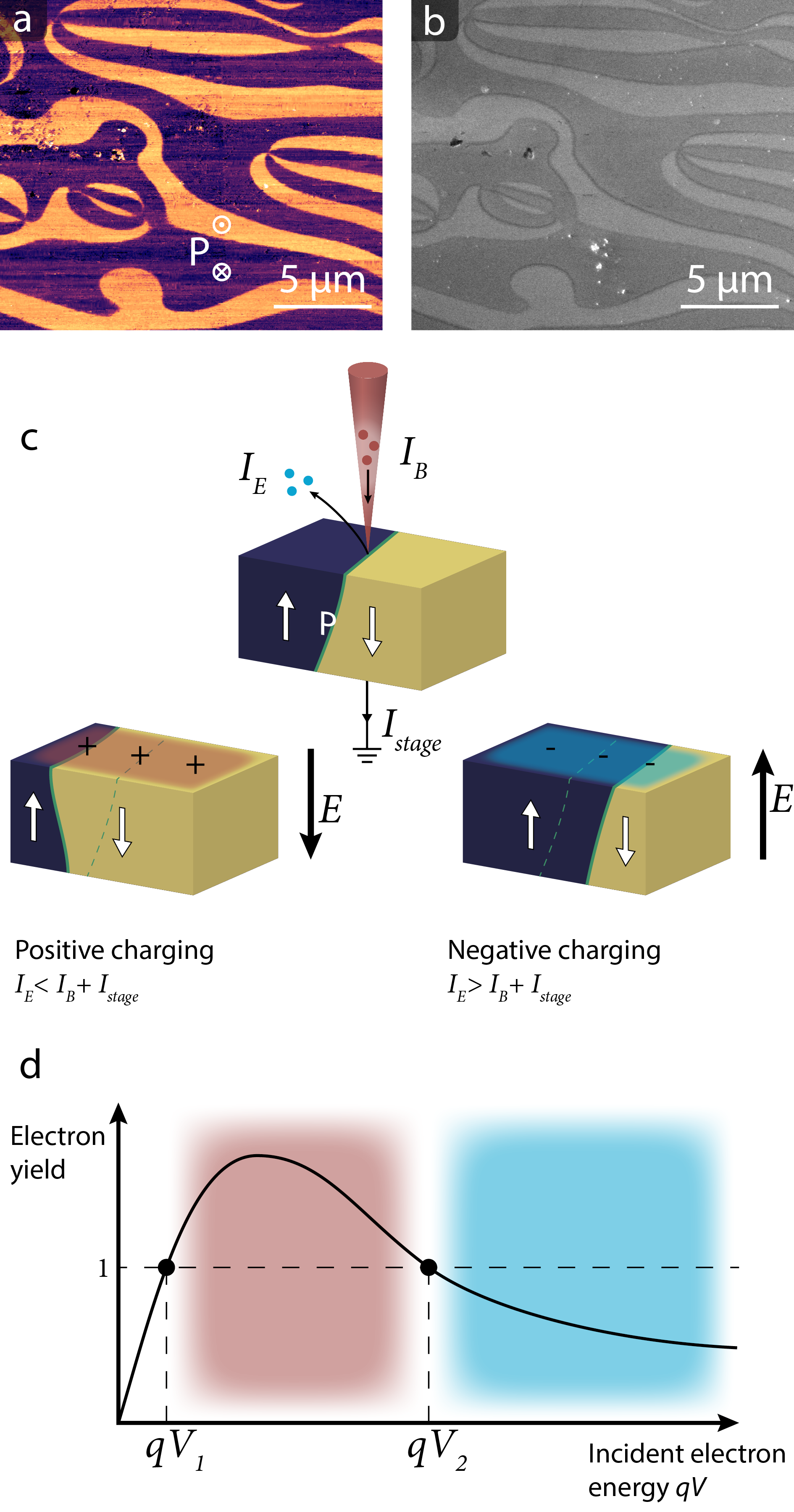
Figure 1 introduces the general approach for domain imaging and switching applied in this study. Figure 1 (a,b) shows the characteristic ferroelectric domain structure of \ceErMnO3 obtained on a polar surface (out-of-plane polarization) using (a) piezoresponse force microscopy (PFM) (dual-AC resonance tracking PFM at peak-to-peak) and (b) SEM ( acceleration voltage, nominal beam current, in-lens secondary electron detector), respectively. Comparison of the two images demonstrates that both PFM and SEM are sensitive to the ferroelectric domain distribution in \ceErMnO3Li et al. (2012); Cheng et al. (2015); Rayapati et al. (2020). In contrast to PFM, where image formation relies on differences in the electromechanical response of P domains, SEM exploits differences in electron emission yield, allowing high-resolution microscopy experiments without the need for electrical contacts. The imaging rate of SEM is also higher than SPM, which allows capturing the dynamics with better time resolution. Under the imaging conditions applied in Figure 1 (b), we find that P domains (bright) have a larger secondary electron yield than P domain (dark). This correlation between SEM contrast and polarization direction holds if imaging parameters are kept constant and can therefore be used to track changes in the domain structure. See, e.g., ref. Hunnestad et al. (2020) for a more detailed discussion of SEM domain and domain wall contrast in ferroelectrics.
Our strategy for generating the positive and negative electric fields required for controlling the improper ferroelectric domains in \ceErMnO3 is presented in Figure 1 (c), showing schematically how irradiation with charged particles can lead to either negative (electron) or positive (electron and \ceGa+) surface charging. Charging in SEM is conventionally explained by the electron yield as a function of incident electron energy , where is the acceleration voltage. In general, two characteristic voltages and exist where the beam current is balanced by the emitted electron current and the leakage current . In our experiments, stable SEM imaging with minimal charging artifacts is achieved around , indicating this is close to . For lower and higher acceleration voltages, the surface charges positively and negatively, respectively, leading to pronounced electric fields that can be used for controlling ferroelectric domains. While domain switching in ferroelectrics has been demonstrated separately using FIB, SEM and TEM Vlasov et al. (2018); McGilly et al. (2017); Chen et al. (2016); Hart et al. (2016), the combination of FIB and SEM enables in-situ investigations of the domain response in 3D, as demonstrated in the following.
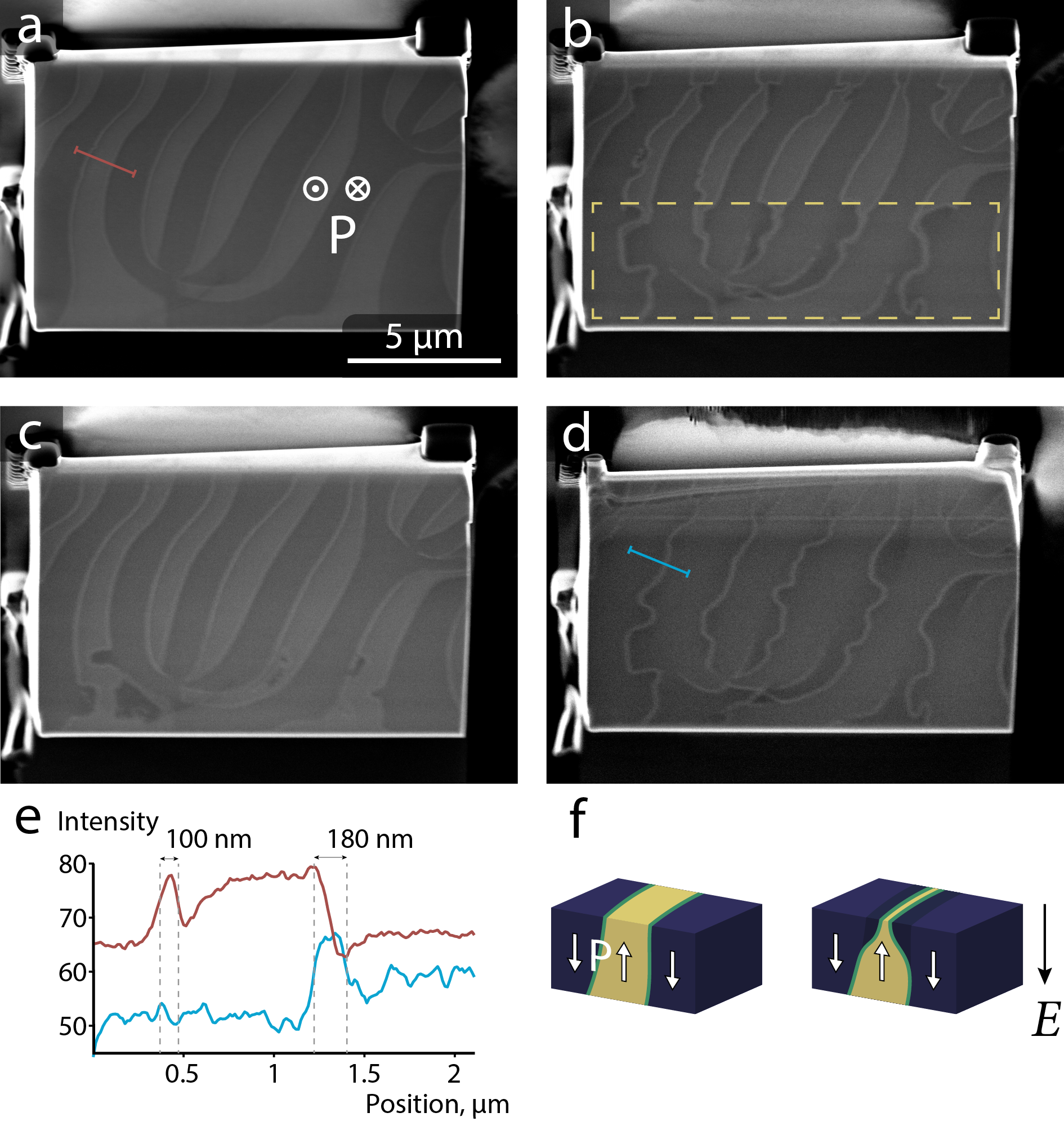
To analyse the response of ferroelectric domains to electron and ion irradiation in a specimen with out-of-plane polarization, Figure 2 (a-d) shows an SEM image series recorded on a plan-view lamella (thickness ) welded to a gold-coated \ceSi substrate. Figure 2 (a) presents the initial ferroelectric domain structure obtained under the same imaging conditions as in Figure 1 (b). Figure 2 (b) shows the same area after exposing the lower part (highlighted by the yellow dashed rectangle) of the sample surface to the \ceGa+ ion beam. The P domains in the exposed area have contracted to meandering bands (we note that the original domain structure appears to be still visible, retraced by a rather faint dark contrast, which will be discussed later on). A recovery of the original domain structure is achieved by repeated imaging at , leading to the domain structure in Figure 2 (c). A comparison of Figures 2 (a) and (c) indicates that the domain walls have returned to their original positions, with only a few exceptions in the lower part of the image. The observed domain wall pinning in this area suggests the presence of defects, causing domain wall roughening Paruch and Guyonnet (2013); Småbråten et al. (2020). A likely source is implanted \ceGa+ ions or structural defects originating from the ion irradiation. Independent of the observed local pinning, however, repeated exposure to the \ceGa+ ion beam allows driving the system back into the same poled state observed initially, as can be seen in Figure 2 (d), showing the domain structure after exposure of the entire lamella to the ion beam. This domain poling behavior, here driven by \ceGa+ exposure, is consistent with previous SPM-based poling experimentsJungk et al. (2010); Choi et al. (2010).
Intensity profiles (averaged over 15 pixels width) taken along the red and blue lines marked in 2 (a) and (d) are displayed in Figure 2 (e), showing that the P domains contract to a width of approximately . This is slightly larger than in previous TEM- and AFM-based investigations, which reported a domain width of Jungk et al. (2010) for electrically poled hexagonal manganites. However, the intensity profile from the as-grown domains shows that individual domain walls display a characteristic SEM signature, which extends over a length scale of about wide. We note that the latter is purely an SEM effect and can be explained based on the potential step between P and domains, as discussed in detail in ref. Nepijko, Sedov, and Schonhense (2001), and is not related to the actual width of the wallsHoltz et al. (2017). Thus, Figure 2 (d) indicates that the domains are either fully poled or at least close to being fully poled. Although the electric fields generated by ion irradiation are difficult to quantify reliably, this observation leads us to the conclusion that they are comparable to the electric field required to achieve saturation polarization of the surface domains, which has been reported to be on the order of . Kuerten et al. (2020)
Upon closer inspection and comparison of the as-grown and poled domain structures, we find that the contracted domains form meandering lines that tend to follow the domain wall positions associated with the as-grown domain structure. This suggests that the domains do not shrink symmetrically, but rather tend to keep one domain wall at its original position. A possible explanation for this behavior is the interaction of the domain walls with intrinsic point defects, promoting domain wall pinningSmåbråten et al. (2020). Aside from the asymmetric domain switching, the SEM data shows a dark contrast around the contracted P domains as briefly mentioned above. We propose that this contrast originates from the subsurface domain morphology as sketched in Figure 2 (f). Analogous to the work by Kuerten et al.Kuerten et al. (2020), it is likely that switching occurs only near the sample surface. As a consequence, the domain walls bent away from their ideal charge-neutral state form positively charged head-to-head walls, which could alter the electrostatic conditions near the surface and thereby the local electron yield. Another possibility is the switching revealing the unscreened polarization charge at the surface.
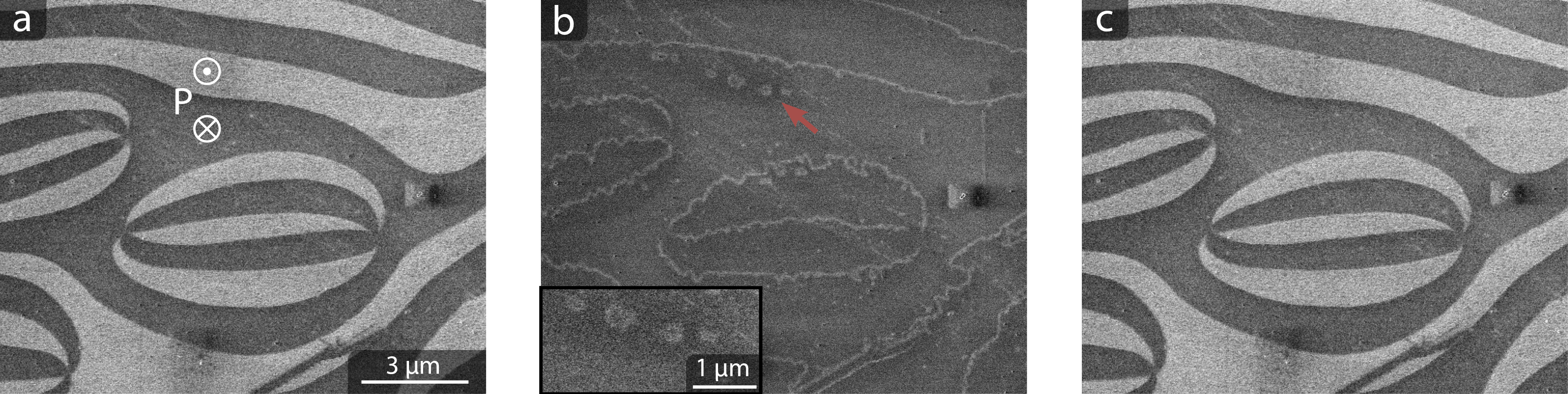
In order to avoid the possibility of ion-beam related domain wall pinning (as suggested by Figure 2), we also investigate reversible domain switching purely via electron irradiation. As illustrated in Figure 1 (d), electron irradiation can lead to both negative and positive surface charging, depending on the incident energy . The corresponding switching experiment is shown in Figure 3. Figure 3 (a) is obtained at , showing the as-grown domain structure, analogous to Figure 1 (b). In contrast to imaging at , however, continuous imaging at lower voltage causes positive charging, leading to polarization switching as presented in Figure 3 (b). Qualitatively, we observe the same behaviour as for ion beam-induced switching (Figure 2), that is, P domains contracting to narrow lines at the surface. The SEM image shown in Figure 3 (c) is also recorded at , but immediately after repeated imaging at , which neutralizes the positive charge that has previously built up. Comparison of Figures 3 (a) and (c) show that by removing the surface charges, the original domain state can be fully restored. Close inspection of Figure 3 (b) shows that in addition to the line-shaped domains, loop-shaped domains are created as shown in the inset. The formation of these loop-shaped domains cannot be explained by domain wall movement alone, demonstrating that polarization reversal also occurs via the nucleation and growth mechanism.
In summary, the switching experiments in Figures 2 and 3 demonstrate that both ion and electron beam irradiation can be used to switch the improper ferroelectric domains in \ceErMnO3. By irradiating the sample with electrons with an energy (non-charging conditions), the as-grown domain state is recovered. The results are consistent with the switching behavior observed when using electrical contacts Jungk et al. (2010); Han et al. (2013); Kuerten et al. (2020), and can be explained assuming partial domain reversal at the surface and in surface-near regions as illustrated in Figure 2 (f).
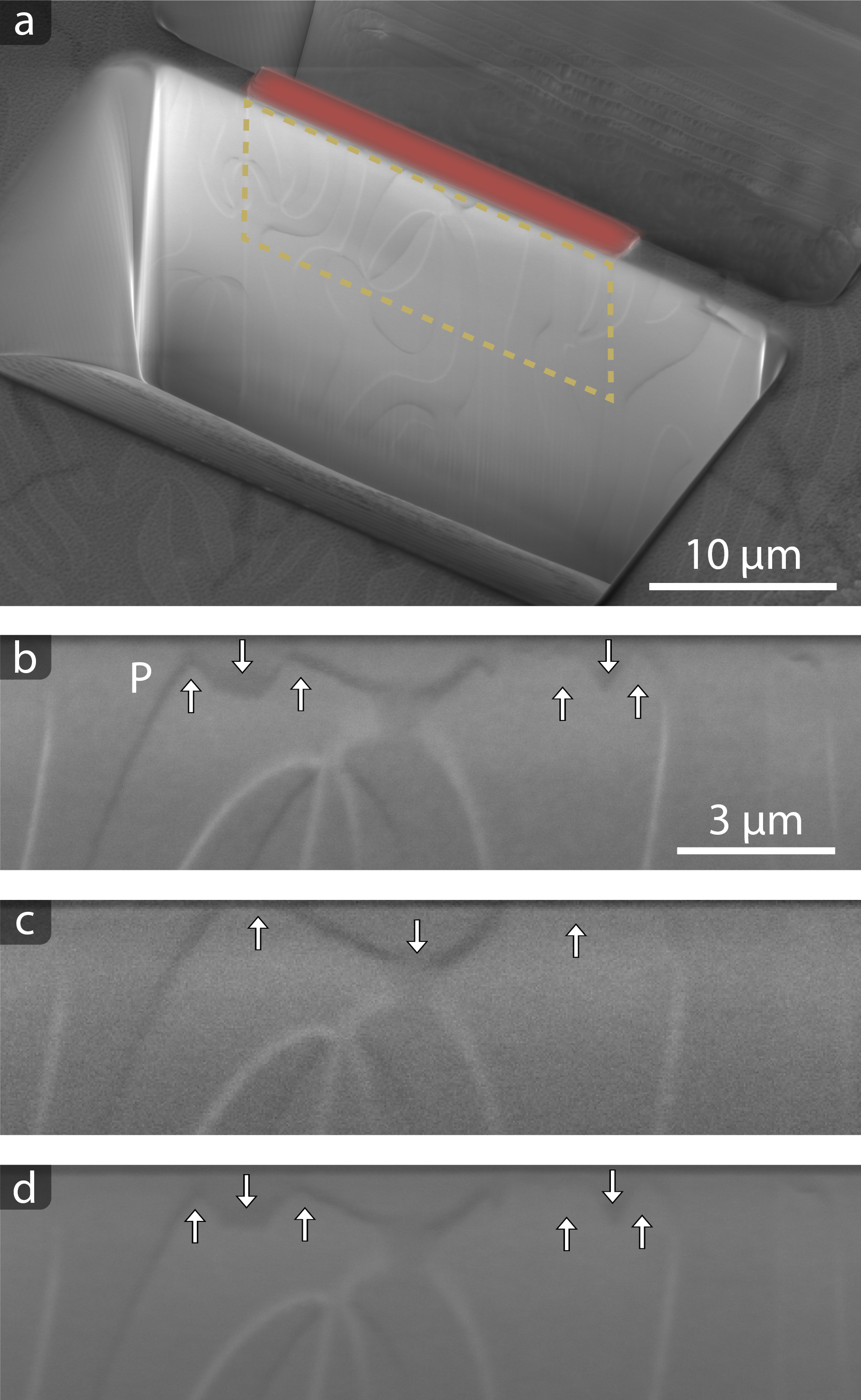
To verify the hypothesis of partially switched domains near the surface and gain insight into the sub-surface switching behaviour, we prepare a cross-sectional lamella with in-plane polarization by FIB-milling of trenches in an out-of-plane polarized crystal, shown in Figure 4 (a). Figure 4 (b) shows the lamella face (marked by the yellow dashed rectangle in Figure 4 (a)) imaged at . The polarization directions are indicated by the arrows. In this orientation, no domain contrast is visible. Instead, we see only the domain walls with distinct contrast between the head-to-head and tail-to-tail domain walls. The dark walls are insulating head-to-head walls, while the bright are conductive tail-to-tail walls Mosberg et al. (2019). The domain configuration in Figure 4 (b) is observed after cutting out the lamella, i.e., after irradiating the top polar face (marked red in Figure 4 (a)) with the \ceGa+ beam, inducing positive surface charging and contraction of P domains as presented in Figure 2. Importantly, the cross-sectional SEM data shows that the domains have indeed only switched in the region near the surface, extending down to around . Under repeated SEM scanning of the lamella face at (i.e. electron irradiation removing the positive surface charge), the domains expand again, and a more balanced distribution of P and P domains in the top part of the lamella is restored (see Figure 4 (c)). The partially poled surface state shown in Figure 4 (d) is reached again after irradiating the top of the lamella with \ceGa+.
III Summary and Outlook
Our results show that charged particle irradiation is a viable method for controlling improper ferroelectric domains in \ceErMnO3. In particular, we find that charging the surface directly allows for bypassing barrier layer effects which arise when using metallic contacts and have prevented the domain control at room temperature in previous studies Ruff et al. (2018); Kuerten et al. (2020). An open challenge associated with the irradiation approach as used here is, however, to adequately estimate the emergent electrical fields, which currently prohibits quantitative measurements.
A back-of-the-envelope estimate made based on the imaging parameters used in Figure 3 (beam current: , pixel size: , dwell time: ) suggests that each scan enhances the surface charge density by about . This plane charge corresponds to an electric field of in vacuum, which exceeds the coercive field of \ceErMnO3 ()Han et al. (2013). We note, however, that leakage currents, as well as electron emission and recapture drastically alter the charging conditions, and need to be controlled adequately in order to enable future quantitative measurements.
In conclusion, the combination of FIB and SEM enables contact-free manipulation of improper ferroelectric domains and analysis of their switching dynamics in 3D. We have demonstrated that polarization reversal in \ceErMnO3 occurs via both movement of domain walls and nucleation and growth of new domains, clarifying the switching behavior at the level of the domains. The possibility of in-situ nanostructuring with FIB allows for varying the boundary conditions, providing new opportunities for studying ferroelectric domain switching in confined geometries without the need for electrical contacts.
Acknowledgements.
The authors acknowledge NTNU for support through the Enabling technologies: NTNU Nano program, the Onsager Fellowship Program and NTNU Stjerneprogrammet. The Research Council of Norway is acknowledged for financial support to the Norwegian Micro- and Nano-Fabrication Facility, NorFab, project number 245963/F50. D.M. further acknowledges funding from the European Research Council (ERC) under the European Union’s Horizon 2020 research and innovation programme (Grant agreement No. 863691). Z.Y. and E.B. were supported by the U.S. Department of Energy, Office of Science, Basic Energy Sciences, Materials Sciences and Engineering Division under Contract No. DE-AC02-05-CH11231 within the Quantum Materials Program-KC2202.IV Data Availability Statement
The data that support the findings of this study are available from the corresponding author upon reasonable request.
V References
References
- Arimoto and Ishiwara (2004) Y. Arimoto and H. Ishiwara, MRS Bulletin 29, 823 (2004).
- Garcia and Bibes (2014) V. Garcia and M. Bibes, Nature Communications 5 (2014).
- Si et al. (2019) M. Si, A. K. Saha, S. Gao, G. Qiu, J. Qin, Y. Duan, J. Jian, C. Niu, H. Wang, W. Wu, S. K. Gupta, and P. D. Ye, Nature Electronics 2, 580 (2019).
- Kakekhani and Ismail-Beigi (2015) A. Kakekhani and S. Ismail-Beigi, ACS Catalysis 5, 4537 (2015).
- Tagantsev, Cross, and Fousek (2010) A. K. Tagantsev, L. E. Cross, and J. Fousek, Domains in Ferroic Crystals and Thin Films (Springer New York, 2010).
- Evans et al. (2020) D. M. Evans, V. Garcia, D. Meier, and M. Bibes, Physical Sciences Reviews 5 (2020).
- Meier, Seidel, and Gregg (2020) D. Meier, J. Seidel, and M. Gregg, Domain Walls: From Fundamental Properties to Nanotechnology Concepts (Oxford University Press, 2020).
- Meier et al. (2009a) D. Meier, M. Maringer, T. Lottermoser, P. Becker, L. Bohatý, and M. Fiebig, Physical Review Letters 102 (2009a).
- Meier et al. (2009b) D. Meier, N. Leo, M. Maringer, T. Lottermoser, M. Fiebig, P. Becker, and L. Bohatý, Physical Review B 80 (2009b).
- Meier et al. (2012) D. Meier, J. Seidel, A. Cano, K. Delaney, Y. Kumagai, M. Mostovoy, N. A. Spaldin, R. Ramesh, and M. Fiebig, Nature Materials 11, 284 (2012).
- Wu et al. (2012) W. Wu, Y. Horibe, N. Lee, S.-W. Cheong, and J. R. Guest, Physical Review Letters 108 (2012).
- Huang et al. (2016) F. T. Huang, F. Xue, B. Gao, L. H. Wang, X. Luo, W. Cai, X. Z. Lu, J. M. Rondinelli, L. Q. Chen, and S. W. Cheong, Nature Communications 7 (2016).
- Matsubara et al. (2015) M. Matsubara, S. Manz, M. Mochizuki, T. Kubacka, A. Iyama, N. Aliouane, T. Kimura, S. L. Johnson, D. Meier, and M. Fiebig, Science 348, 1112 (2015).
- McQuaid et al. (2017) R. G. McQuaid, M. P. Campbell, R. W. Whatmore, A. Kumar, and J. M. Gregg, Nature Communications 8, 15105 (2017).
- Coeuré et al. (1966) P. Coeuré, F. Guinet, J. C. Peuzin, G. Buisson, and E. F. Bertaut, Proc. Int. Meet. Ferroelectr. 1 (1966).
- Meier et al. (2013) D. Meier, M. Lilienblum, P. Becker, L. Bohatý, N. Spaldin, R. Ramesh, and M. Fiebig, Phase Transitions 86, 33 (2013).
- Aken et al. (2004) B. B. V. Aken, T. T. Palstra, A. Filippetti, and N. A. Spaldin, Nature Materials 3, 164 (2004).
- Fennie and Rabe (2005) C. J. Fennie and K. M. Rabe, Physical Review B 72 (2005).
- Bertaut, Forrat, and Fang (1963) F. Bertaut, F. Forrat, and P. Fang, Comptes rendus hebdomadaires des séances de l’Académie des Sciences 256, 1958 (1963).
- Šafránková, Fousek, and Kižaev (1967) M. Šafránková, J. Fousek, and S. A. Kižaev, Czechoslovak Journal of Physics 17, 559 (1967).
- Choi et al. (2010) T. Choi, Y. Horibe, H. T. Yi, Y. J. Choi, W. Wu, and S.-W. Cheong, Nature Materials 9, 253 (2010).
- Jungk et al. (2010) T. Jungk, Á. Hoffmann, M. Fiebig, and E. Soergel, Applied Physics Letters 97, 012904 (2010).
- Yang et al. (2017) K. L. Yang, Y. Zhang, S. H. Zheng, L. Lin, Z. B. Yan, J.-M. Liu, and S.-W. Cheong, Physical Review B 96 (2017).
- Han et al. (2013) M.-G. Han, Y. Zhu, L. Wu, T. Aoki, V. Volkov, X. Wang, S. C. Chae, Y. S. Oh, and S.-W. Cheong, Advanced Materials 25, 2415 (2013).
- Ruff et al. (2018) A. Ruff, Z. Li, A. Loidl, J. Schaab, M. Fiebig, A. Cano, Z. Yan, E. Bourret, J. Glaum, D. Meier, and S. Krohns, Applied Physics Letters 112, 182908 (2018).
- Kuerten et al. (2020) L. Kuerten, S. Krohns, P. Schoenherr, K. Holeczek, E. Pomjakushina, T. Lottermoser, M. Trassin, D. Meier, and M. Fiebig, Physical Review B 102 (2020).
- Schoenherr et al. (2019) P. Schoenherr, K. Shapovalov, J. Schaab, Z. Yan, E. D. Bourret, M. Hentschel, M. Stengel, M. Fiebig, A. Cano, and D. Meier, Nano Letters 19, 1659 (2019).
- Yan et al. (2015) Z. Yan, D. Meier, J. Schaab, R. Ramesh, E. Samulon, and E. Bourret, Journal of Crystal Growth 409, 75 (2015).
- Mosberg et al. (2019) A. B. Mosberg, E. D. Roede, D. M. Evans, T. S. Holstad, E. Bourret, Z. Yan, A. T. J. van Helvoort, and D. Meier, Applied Physics Letters 115, 122901 (2019).
- Reimer (2010) L. Reimer, Scanning Electron Microscopy (Springer Berlin Heidelberg, 2010).
- Li et al. (2012) J. Li, H. X. Yang, H. F. Tian, C. Ma, S. Zhang, Y. G. Zhao, and J. Q. Li, Applied Physics Letters 100, 152903 (2012).
- Cheng et al. (2015) S. Cheng, S. Q. Deng, W. Yuan, Y. Yan, J. Li, J. Q. Li, and J. Zhu, Applied Physics Letters 107, 032901 (2015).
- Rayapati et al. (2020) V. R. Rayapati, D. Bürger, N. Du, C. Kowol, D. Blaschke, H. Stöcker, P. Matthes, R. Patra, I. Skorupa, S. E. Schulz, and H. Schmidt, Nanotechnology 31, 31LT01 (2020).
- Hunnestad et al. (2020) K. A. Hunnestad, E. D. Roede, A. T. J. van Helvoort, and D. Meier, Journal of Applied Physics 128, 191102 (2020).
- Vlasov et al. (2018) E. Vlasov, D. Chezganov, M. Chuvakova, and V. Y. Shur, Scanning 2018, 1 (2018).
- McGilly et al. (2017) L. J. McGilly, C. S. Sandu, L. Feigl, D. Damjanovic, and N. Setter, Advanced Functional Materials 27, 1605196 (2017).
- Chen et al. (2016) Z. Chen, X. Wang, S. P. Ringer, and X. Liao, Physical Review Letters 117 (2016).
- Hart et al. (2016) J. L. Hart, S. Liu, A. C. Lang, A. Hubert, A. Zukauskas, C. Canalias, R. Beanland, A. M. Rappe, M. Arredondo, and M. L. Taheri, Physical Review B 94 (2016).
- Paruch and Guyonnet (2013) P. Paruch and J. Guyonnet, Comptes Rendus Physique 14, 667 (2013).
- Småbråten et al. (2020) D. R. Småbråten, T. S. Holstad, D. M. Evans, Z. Yan, E. Bourret, D. Meier, and S. M. Selbach, Physical Review Research 2 (2020).
- Nepijko, Sedov, and Schonhense (2001) S. A. Nepijko, N. N. Sedov, and G. Schonhense, Journal of Microscopy 203, 269 (2001).
- Holtz et al. (2017) M. E. Holtz, K. Shapovalov, J. A. Mundy, C. S. Chang, Z. Yan, E. Bourret, D. A. Muller, D. Meier, and A. Cano, Nano Letters 17, 5883 (2017).