The Optimal Location and Size of an Intermediate Coil in a Magnetic Resonant Coupling Wireless Power Transfer System
Abstract
To increase the transmission distance of Wireless Power Transfer (WPT) systems, we provide guidelines on choosing the optimal location of an Intermediate Coil with respect to size within a standard five-coil axially aligned experimental setup. From our results, for maximum magnitude of S21 at the resonant frequency we found the optimal location to exist where the coupling coefficient between the Transmitter and the Intermediate Coil and the coupling coefficient between the Receiver and the Intermediate Coil are identical. Additionally, the optimal outer diameter for the maximum magnitude of S21 at the resonant frequency of the Intermediate Coil in the given symmetric and asymmetric setup are found to be larger than both TX and RX.
Index Terms:
Intermediate Coil, Magnetic Resonant Coupling, Optimal Intermediate Coil Size, Optimal Intermediate Coil Location, Wireless Power TransferI Introduction
In recent years, studies in WPT have been focused on its application in the near field, such as close-range WPT that adopts the magnetic inductive coupling [1, 2, 3, 4] or mid-range WPT which utilizes Magnetic Resonant Coupling (MRC) [5, 6, 7, 8, 9, 10]. Applications range from the supplying power to commuter busses [11] all the way down to human implantable devices [12] and across many formerly hostile environments such as ocean going [13] or extraterrestrial based operations [14].
In this paper, the MRC WPT is utilized, such that both transmitter coil (TX), consisting of a loop coil (TXL) and a spiral coil (TXC), and receiver coil (RX), consisting of a loop coil (RXL) and a spiral coil (RXC), are tuned to the same resonant frequency, 13.56MHz. High-power transmission of a MRC WPT system is generally realized within two coil diameters [15], as power transfer efficiency decreases with distance, which does not still satisfy the desires of the consumer market since the diameter of the coils are generally in mm-scale. The effects of Intermediate Coils (ICs) have been shown as a means to increase the transmission distance [16, 17], and alternative designs of such a system consisting of ICs has been proposed [18, 19]. While previous works have shown that the proper addition of one or more ICs could increase transmission distance, power transfer efficiency, and the transferred power to a conventional four-coil system, for maximum transferred power the optimal location and size for an IC are not covered.
In this paper, we will show the optimal location and size of an IC that gives the maximum transferred power in the MRC WPT system. The five-coil system used here, i.e. TXL-TXC-IC-RXC-RXL (as shown in Fig. 1), is analyzed by using circuit theory in Section II. To determine the parameters that maximize the power transferred to the load, the magnitude of scattering parameter S21 is quantitatively simulated and experimentally measured. Because multiple resonant frequencies will appear when coils are over coupled (so called frequency splitting in [7]), we chose to collect the S21 data at the designed resonant frequency, since such frequency will provide the maximum magnitude of S21 in the system of odd number of coils [17]. A symmetric and an asymmetric system have been designed, the former consists of identical TX and RX while the latter consists of a TX OD that is 3x larger than the RX OD. The system setups, including the experimental setup and quantitative simulation setup, are demonstrated in Section III. Then, in Section IV, the optimal location of ICs of varying sizes in both systems are provided, and simulation and experimental results are compared.
This paper provides guidance for the optimal location of an IC in the five-coil MRC WPT system, whether symmetric or asymmetric. Additionally to the optimal location, this paper reports the optimal size of the IC with the given experimental setup.
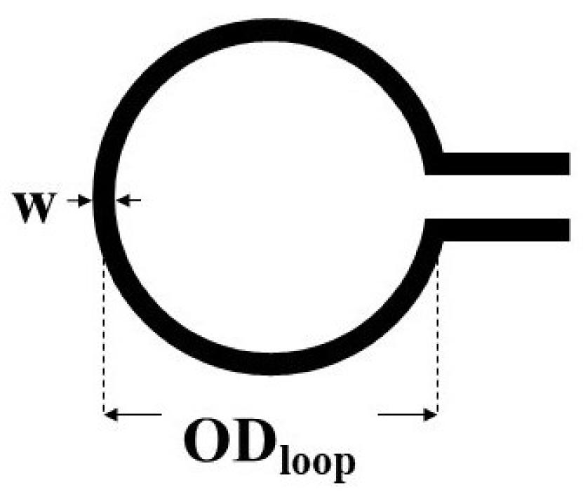
II System Analysis
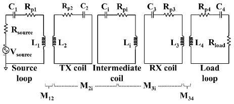
With the presence of an IC, the conventional four-coil system (loop-coil-coil-loop) becomes a five-coil system (loop-coil-intermediate-coil-loop). Then, the system is analyzed using the circuit theory so that the quantitative model can be compared with the experiment and determine the generalizability of the system. In Fig. 3, the system circuit model is shown and all parasitic or designed components are indicated by lumped elements R, L, and C. The Source loop (TXL) and Load loop (RXL) are loop coils consisting of a single turn (shown in Fig. 2(a)), the former connecting to a voltage source, Vsource, with a source impedance, Rsource, and the latter connecting to a load, Rload. L1, L4 and Rp1, Rp4 designate self-inductance and parasitic resistances of the two loop coils respectively, and C1, C4 designate the tuned capacitance, which set the loop coils to resonate at the designed frequency. The TX Coil (TXC), IC, and RX Coil (RXC) are multi-turn single layer spiral coils that have self-inductance of L2, Li, L3 and parasitic resistance of Rp2, Rpi, Rp3, respectively. Capacitors C2, Ci, C3 are added to tune the spiral coils to the resonant frequency. M12 and M34 are the mutual inductance (M) between TXL and TXC and between the RXL and RXC, respectively. M2i and M3i are the M between TXC and IC and between the RXC and IC. The M of nonadjacent elements are neglected, e.g. M14, M13, etc., as they are minuscule by comparison [7].
| (1) |
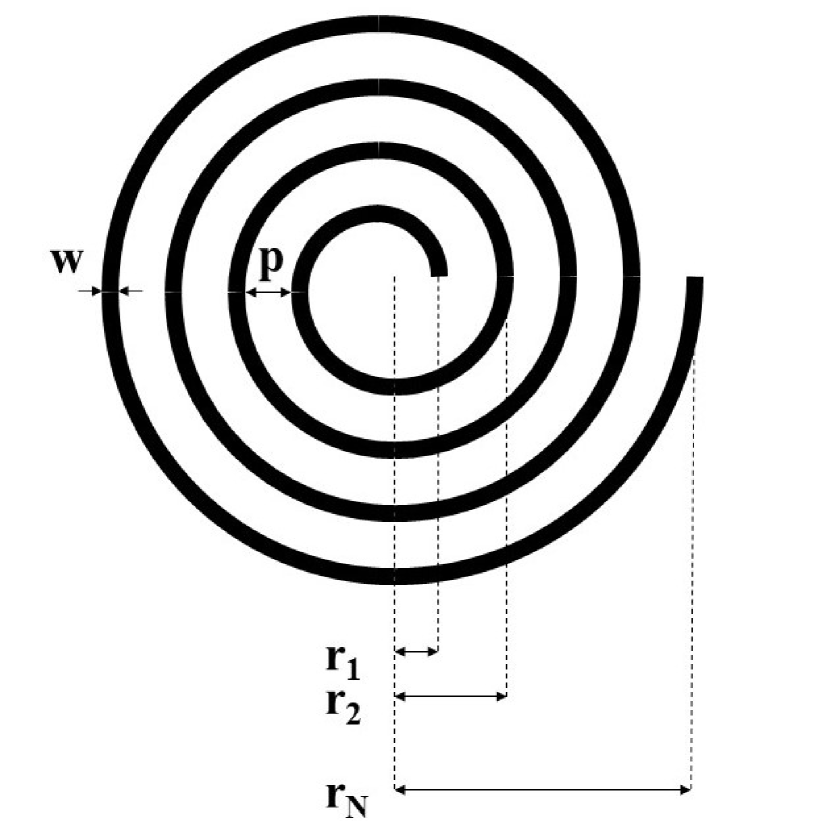
The generalized self-inductance L is defined by the geometry of a coil. As shown in Fig. 2, parameters of both loop coil and multi-turn single layer spiral coil are defined. In Fig. 2(a), ODloop and w indicate the OD of the loop coil and the wire diameter respectively. In Fig. 2(b), w, N, p, and RN indicate the wire diameter, the number of turns, distance between each turn, and the radius of Nth turn respectively. The inner diameter, IDspiral, and the outer diameter, ODspiral, of a spiral coil is defined in (1). All units of length are in meters.
The equation for the Lx of spiral coils (2a) is defined in [20], which is a modified form of Wheeler’s formula. For loop coils (2b), it’s a modified form of Kirchhoff’s formula which can be found in [21]. In both, the inductance is measured in Henries.
| (2a) | ||||
| (2b) | ||||
The generalized equation for MAB from [20] is modified by summing all the mutual inductances of ith turn of the primary coil A to jth turn of the secondary coil B 3, and has units of Henries. The radii rAi and rBj, NA and NB define the geometry of the two coils, d indicates the distance between them, and is the free space permeability.
| (3) | ||||
The coupling coefficient [7] is proportional to the mutual inductance between the primary and the secondary coils (4), normalized by the self-inductances.
| (4) |
The tuned capacitance (5) is defined by the equation of resonant frequency of RLC circuits and its value is assumed to be dominant as it is generally large enough that the self-capacitance of a coil is negligible [20] addition. The f0 in the equation indicates the designed resonant frequency, and the unit of capacitance is in Farad.
| (5) |
The parasitic resistance of a coil, Rp (6a), consists of both a conductive as well as radiative loss[22]. The frequency dependent conduction loss at high frequencies is better described as the resistive skin effect, Rskin (6c), which modifies RDC (6b) to account for shell distribution of current within in a wire at high frequencies. The radiative proximity effect loss, Rproximity, results from the electron crowding due to EM fields of nearby wires within a given coil (6d).
| (6a) | ||||
| (6b) | ||||
| (6c) | ||||
| (6d) | ||||
Where is the copper’s conductivity, denotes the skin depth.
By applying Kirchhoff’s Voltage Law (KVL), the relationship between current and voltage in each coil is shown in (7).
| (7) |
Then the ratio of load to source voltage provides the voltage gain, as solved from (7), and yields (14).
| (14) |
The impedances along the diagonal in (7), e.g. Z11 to Z44, represent the self-impedance of each coil, which consist of both resistance and reactance as detailed in (15).
| (15) |
By contrast the off-diagonal elements of (14), e.g. Z12 or Z2i, are the mutual-impedance of two adjacent coils. They can be substituted for MAB via (16) [23].
| (16) |
Finally, the scattering parameter S21 (17) can be can be derived from (14) by using [7]. Note that the S21 generally refers to the power received by port 2 from port 1, which is the power received by load from source in our system, and is thus designated here in order to stick to accepted nomenclature.
| (17) |
III System Setup
III-A Experimental Setup
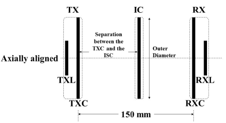
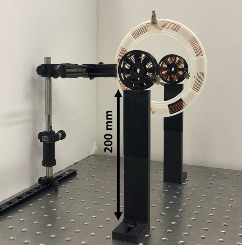
To minimize sources of variation, all of the coils have been designed to have exactly seven turns, using the same wire diameter of the same wire type of wire (Magnet wire, 20 AWG), and having the same distance between each turn. Therefore, the primary independent variable for each coil is their OD. Fig. 1 is an aerial view for both symmetric and asymmetric systems, and all loops and coils are axially aligned. The separation between TXL and TXC, as well as RXL and RXC, is held at the distance where S11 is minimized (symmetric separation = 2.5mm, whereas in the asymmetric system, the large coil’s separation = 10mm and the small coil’s separation = 2mm). Using the above biased TX and RX in a series resonant circuit allows for the doubling of the coupling coefficient [17], and therefore is advantageous when attempting to maximize transferred power over longer separations between TX and RX.
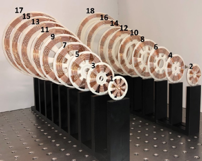
The distance between the face of TX and RX, and therefore also TXC and RXC, is a constant 150mm. We sweep the IC from one end to the other, and its location along the axis is denoted by the separation between the TX and the IC. All coils are 200 mm above the metal experimental platform so that it will not interfere the WPT system. As show in Fig. 4, we had designed ICs with ODs from 30 to 200 mm at 10 mm interval. Fig. 5 shows the experimental set-up of the symmetric system where the TX and the RX are identical. In this symmetric system, as a reference for this work, both the TXC and RXC are designed to be multi-turn single layer spiral coils that have a 50 mm outer diameter. Both TXL and RXL are loop coils that have a 38 mm OD. In the case of the asymmetric system, we have designed the OD of the TXC is 90 mm, that of the RXC is 30 mm, that of the TXL is 67.5 mm, and that of the RXL is 10.44 mm. The OD of the spiral coils to be tested was chosen to ensure the TX and RX are weakly coupled. Thus, the OD of TX was chosen to have a critical coupling distance of around 1/5 the TX to RX separation (150mm), where the critical coupling distance is [15]. Then, the OD of RSC was chosen to be the minimum size possible while maintaining the same coil geometric associations (i.e. wire diameter, number of turns, and the separation between each turn). The scattering parameter S21 is measured by the HP8753E Vector Network Analyzer (VNA) at the designed resonant frequency.
III-B Quantitative Simulation Setup
To provide additional insight towards optimal IC location and size selection, the chain of analysis followed in Section II was replicated in Matlab to mimic the experimental setup in III-A. Key parameters, such as OD, number of turns, wire diameter, and separation between each turn, have the same values of those in the experimental setup. Within the simulation, the self-inductance (2a) (2b) and mutual inductance (3) are then calculated based on a given coils’ geometry. In order to tune all coils to the designated resonant frequency, the value of tuning capacitance is derived from (5). Finally, from self-impedance (15) and mutual impedance (16) the magnitude of S21 (17) is derived and simulation results are reported alongside the experimental.
IV Experimental and Quantitative Simulation Results
IV-A Symmetric System
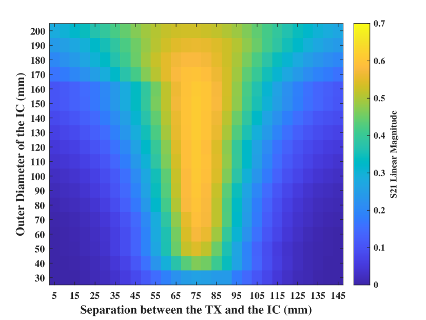
In the symmetric system, Fig. 6 results from sweeping the ICs of different sizes along the axis between the TX and RX. The horizontal axis shows the separation between the TX and the IC. The vertical axis shows the OD of the IC of different sizes. The intensity of color represents the magnitude of S21. The maximum magnitude of S21 within a given separation sweep is always located where the separation between the TX and the IC equals 75mm, which is the center of the TX and RX in the symmetric system, and the coupling coefficient of the TXC and the IC, kTXC-IC, equals the coupling coefficient of the RX and the IC, kRXC-IC. Our simulation shows the maximum magnitude of S21 and equal-coupling points are both located where the IC is centered between the TX and the RX.
IV-B Asymmetric System
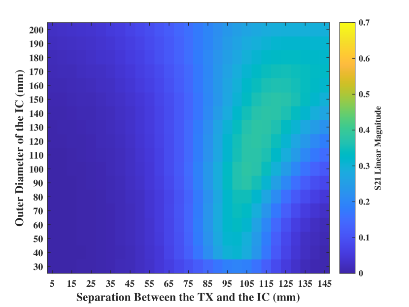
Similar to the symmetric system, Fig. 7 is the result of sweeping ICs of different sizes in the asymmetric system. The maximum magnitude of S21 is always closer to the RX, which is the smaller coil side. This phenomenon has also been analyzed and experimentally shown in [17]. In addition, the location of ICs where maximum S21 present in the asymmetric system gradually shifts closer to the RX as the OD of ICS gets larger. Note, this result is mirrored when RX replaces TX as the the transmitter (i.e. S21 = S12).
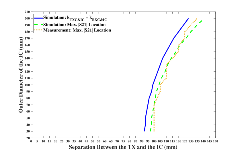
As shown in Fig 8, we compare the location of the kTXC-IC = kRXC-IC in simulation and the location of the IC where the maximum magnitude of S21 present in simulation and measurement. The simulated maximum of S21 location matches with the measured maximum of S21 location in general, and the simulated equal-coupling location is different from the measurement by 6.67% in most of the tested cases because we have neglected the inter-coupling coefficients (kTXL-RXC, kTXL-RXL, etc.).
IV-C Optimal IC Size
While it may seem that a larger IC may result in monotonically increasing magnitude of S21, Fig. 6 and Fig. 7 show experimental results that suggest the optimal size of an IC in both symmetric and asymmetric systems. In Fig. 6 and Fig. 7, the magnitude of S21 will increase with increasing size of ICs up to a given OD, but then continuously decrease after it is larger than a certain size. With the given experimental setup, the optimal size of the IC is OD 150mm for the symmetric system, which is 3x larger than the OD 50mm TXC and RXC, and 140 mm for the asymmetric system, which is 1.6x larger than the OD 90mm TXC and 4.7x larger than the OD 30mm RXC.
V Conclusion
After analyzing the circuit model of the five-coil system, and through the above experiments, quantitatively simulated and experimentally measured results have been compared. We have found that the optimal location of an IC in both symmetric and asymmetric systems is located where the TX and RX are equally coupled to the IC. Then, from the experimental results in the given setup, we have determined that there exists an optimal size of IC in both symmetric system and asymmetric system, and the size is larger than both TX and RX.
Future work includes deriving more explicit formulas for better predicting the optimal size in the above 5-coil setup, and incorporating an optimal separation of the loop and spiral coils for both the TX and RX.
Acknowledgment
This work was supported by Department of Defense Medical Command Award No. W81XWH-20-1-0010 and the Center for Neural Technology (CNT), NSF Grant EEC-1028725, as well as University of Washington Institute for Neuroengineering (UWIN). The authors would also like to specifically thank the members of the Sensor Systems Lab for their help and support in this work, and Han-Ting Lin for his support.
References
- [1] J. T. Boys, G. A. Covic, and A. W. Green, “Stability and control of inductively coupled power transfer systems,” IEE Proceedings - Electric Power Applications, vol. 147, no. 1, pp. 37–43, 2000.
- [2] Byungcho Choi, Jaehyun Nho, Honnyong Cha, Taeyoung Ahn, and Seungwon Choi, “Design and implementation of low-profile contactless battery charger using planar printed circuit board windings as energy transfer device,” IEEE Transactions on Industrial Electronics, vol. 51, no. 1, pp. 140–147, 2004.
- [3] M. Eghtesadi, “Inductive power transfer to an electric vehicle-analytical model,” in 40th IEEE Conference on Vehicular Technology, pp. 100–104, 1990.
- [4] D. van Wageningen and T. Staring, “The qi wireless power standard,” in Proceedings of 14th International Power Electronics and Motion Control Conference EPE-PEMC 2010, pp. S15–25–S15–32, 2010.
- [5] A. Kurs, A. Karalis, R. Moffatt, J. D. Joannopoulos, P. Fisher, and M. Soljačić, “Wireless power transfer via strongly coupled magnetic resonances,” science, vol. 317, no. 5834, pp. 83–86, 2007.
- [6] A. Karalis, J. D. Joannopoulos, and M. Soljačić, “Efficient wireless non-radiative mid-range energy transfer,” Annals of physics, vol. 323, no. 1, pp. 34–48, 2008.
- [7] A. P. Sample, D. T. Meyer, and J. R. Smith, “Analysis, experimental results, and range adaptation of magnetically coupled resonators for wireless power transfer,” IEEE Transactions on industrial electronics, vol. 58, no. 2, pp. 544–554, 2010.
- [8] S. Delichte, Y. Lu, and J. Bobowski, “Non-radiative mid-range wireless power transfer: An experiment for senior physics undergraduates,” American Journal of Physics, vol. 86, no. 8, pp. 623–632, 2018.
- [9] B. L. Cannon, J. F. Hoburg, D. D. Stancil, and S. C. Goldstein, “Magnetic resonant coupling as a potential means for wireless power transfer to multiple small receivers,” IEEE transactions on power electronics, vol. 24, no. 7, pp. 1819–1825, 2009.
- [10] S. Assawaworrarit, X. Yu, and S. Fan, “Robust wireless power transfer using a nonlinear parity–time-symmetric circuit,” Nature, vol. 546, no. 7658, pp. 387–390, 2017.
- [11] Y. D. Ko and Y. J. Jang, “The optimal system design of the online electric vehicle utilizing wireless power transmission technology,” IEEE Transactions on Intelligent Transportation Systems, vol. 14, DOI 10.1109/TITS.2013.2259159, no. 3, pp. 1255–1265, 2013.
- [12] D. A. Borton, M. Yin, J. Aceros, and A. Nurmikko, “An implantable wireless neural interface for recording cortical circuit dynamics in moving primates,” Journal of Neural Engineering, vol. 10, DOI 10.1088/1741-2560/10/2/026010, no. 2, p. 026010, Feb. 2013. [Online]. Available: https://doi.org/10.10882F1741-25602F102F22F026010
- [13] T. M. Hayslett, T. Orekan, and P. Zhang, “Underwater wireless power transfer for ocean system applications,” in OCEANS 2016 MTS/IEEE Monterey, DOI 10.1109/OCEANS.2016.7761481, pp. 1–6, 2016.
- [14] C. Liu, K. T. Chau, Z. Zhang, C. Qiu, F. Lin, and T. W. Ching, “Multiple-receptor wireless power transfer for magnetic sensors charging on mars via magnetic resonant coupling,” Journal of Applied Physics, vol. 117, DOI 10.1063/1.4918624, no. 17, p. 17A743, 2015. [Online]. Available: https://doi.org/10.1063/1.4918624
- [15] R. Shadid and S. Noghanian, “A literature survey on wireless power transfer for biomedical devices,” International Journal of Antennas and Propagation, vol. 2018, 2018.
- [16] F. Zhang, S. A. Hackworth, W. Fu, C. Li, Z. Mao, and M. Sun, “Relay effect of wireless power transfer using strongly coupled magnetic resonances,” IEEE Transactions on Magnetics, vol. 47, no. 5, pp. 1478–1481, 2011.
- [17] D. Ahn and S. Hong, “A study on magnetic field repeater in wireless power transfer,” IEEE Transactions on Industrial Electronics, vol. 60, no. 1, pp. 360–371, 2012.
- [18] X. Zhang, S. Ho, and W. Fu, “Quantitative design and analysis of relay resonators in wireless power transfer system,” IEEE transactions on magnetics, vol. 48, no. 11, pp. 4026–4029, 2012.
- [19] B. Luo, S. Wu, and N. Zhou, “Flexible design method for multi-repeater wireless power transfer system based on coupled resonator bandpass filter model,” IEEE Transactions on Circuits and Systems I: Regular Papers, vol. 61, no. 11, pp. 3288–3297, 2014.
- [20] B. H. Waters, B. J. Mahoney, G. Lee, and J. R. Smith, “Optimal coil size ratios for wireless power transfer applications,” in 2014 IEEE international symposium on circuits and systems (ISCAS), pp. 2045–2048. IEEE, 2014.
- [21] E. B. Rosa and F. W. Grover, Formulas and tables for the calculation of mutual and self-inductance, vol. 8, ch. 5, p. 110. US Government Printing Office, 1948.
- [22] J. Ferreira, “Appropriate modelling of conductive losses in the design of magnetic components,” in 21st Annual IEEE Conference on Power Electronics Specialists, pp. 780–785. IEEE, 1990.
- [23] S. Y. R. Hui, W. Zhong, and C. K. Lee, “A critical review of recent progress in mid-range wireless power transfer,” IEEE Transactions on Power Electronics, vol. 29, no. 9, pp. 4500–4511, 2013.
![[Uncaptioned image]](/html/2012.00244/assets/x10.png) |
Kedi Yan (S’20) was born in Zhengzhou, Henan, China on August 22nd, 1995. He received the B.S. degree in Electrical and Computer Engineering from Oregon State University, Corvallis, OR, USA in 2018. He is currently working toward his M.S. degree in Electrical Engineering at the University of Washington, Seattle, WA, the United State. His research interests include electromagnetism in general, with a special focus on Radio Frequency, Microwave, WPT, WPT to biomedical devices, and Magnetic Nanoparticles. |
![[Uncaptioned image]](/html/2012.00244/assets/x11.png) |
Gregory Moore (M’20) was born in New Orleans, LA, USA. He received his B.S. degree in Physics and B.S. degree in Electrical Engineering from the University of Maryland, College Park, MD, USA in 2005, and the M.S. degree in Electrical Engineering from the University of Washington, Seattle, WA, USA in 2018. From 2008 to 2012 he was with Tao of Systems Integration, Inc., Hampton, VA, USA, where he was engaged mixed signal circuit and control systems design for flow measurement products for the aeronautics/marine engineering. He is currently a Research Assistant at the University of Washington, WA, USA. His research is concerned with WPT and low-power communication design, with special focus on applications directed towards biopotential stimulation, recording, and telemetry. |
![[Uncaptioned image]](/html/2012.00244/assets/x12.png) |
Joshua R. Smith (M’99-SM’12-F’20) was born in Washington, D.C.. He received a B.A. in Computer Science and Philosophy from Williams College, Williamstown, MA, USA in 1991, an M.A. in Physics from the University of Cambridge, Cambridge, UK in 1997, and S.M. and Ph.D. degrees from the Media Laboratory at the Massachusetts Institute of Technology, Cambridge, MA, USA in 1995 and 1999. He is the Milton and Delia Zeutschel Professor, jointly appointed in Computer Science and Engineering and in Electrical and Computer Engineering at the University of Washington. He is a founder of three companies: Wibotic, Jeeva Wireless, and Proprio. Previously he was a Principal Engineer at Intel Corp. Professor Smith was elevated to IEEE Fellow for contributions to far- and near-field wireless power, backscatter communication, and electric field sensing. He is interested in all aspects of sensor systems, including wireless methods for powering and communicating with sensors, and applications including ubiquitous computing, biomedical implants, and robotics. |