Electron-hole asymmetry and band gaps of commensurate double moire patterns in twisted bilayer graphene on hexagonal boron nitride
Abstract
Spontaneous orbital magnetism observed in twisted bilayer graphene (tBG) on nearly aligned hexagonal boron nitride (BN) substrate builds on top of the electronic structure resulting from combined G/G and G/BN double moire interfaces. Here we show that tBG/BN commensurate double moire patterns can be classified into two types, each favoring the narrowing of either the conduction or valence bands on average, and obtain the evolution of the bands as a function of the interlayer sliding vectors and electric fields. Finite valley Chern numbers are found in a wide range of parameter space when the moire bands are isolated through gaps, while the local density of states associated to the flat bands are weakly affected by the BN substrate invariably concentrating around the AA-stacked regions of tBG. We illustrate the impact of the BN substrate for a particularly pronounced electron-hole asymmetric band structure by calculating the optical conductivities of twisted bilayer graphene near the magic angle as a function of carrier density. The band structures corresponding to other -multiple commensurate moire period ratios indicate it is possible to achieve narrow width meV isolated folded band bundles for tBG angles .
I Introduction
The electronic properties of magic angle twisted bilayer graphene (tBG) and other graphene moire systems have become an intense focus of research in recent years after observations of strong correlations and superconductivity in transport experiments Cao et al. (2018a, b); Kim et al. (2017); Yankowitz et al. (2019); MacDonald (2019); Saito et al. (2020). One of the striking observations revealing the inherent topological character of the bands in graphene moire systems Zhang et al. (2019a); Chittari et al. (2019) is the spontaneous anomalous Hall effects at 3/4 filling in tBG that appear even in the absence of an external magnetic field Sharpe et al. (2019); Lu et al. (2019); Serlin et al. (2020), which can be viewed as a solid state realization of the Haldane-like model in a honeycomb lattice Haldane (1988). Theories attempting to explain the spontaneous Hall effects relied on band structures that included a small mass term in the Dirac Hamiltonian contacting the BN substrate Bultinck et al. (2020); Zhang et al. (2019b) that give rise to precursor bands of the spontaneous quantum Hall phases. The fact that this effect in tBG has been observed so far only in twisted bilayer graphene for samples that are nearly aligned with hexagonal boron nitride (tBG/BN) Tschirhart et al. (2020); Polshyn et al. (2020); He et al. (2020) motivates further research on the effects of the BN substrate in modifying the electronic structure of twisted bilayer graphene.
In this manuscript we show that commensurate double moire patterns of tBG on BN can have significant electron-hole asymmetric bands in addition to gaps between the moire bands which provide the conditions for the formation of valley Chern bands prone to strong correlations. Here we focus our discussions on commensurate double moire patterns of tBG/BN whose continuum Hamiltonian can be conveniently formulated in terms in a unique moire Brillouin zone. The electronic structure of double moire patterns was addressed in the past for arbitrary relative twist angles in systems like BN encapsulated graphene Leconte and Jung (2020); Anđelković et al. (2020); Wang et al. (2019) or twisted trilayer graphene Zhu et al. (2020a) giving rise to super-moire patterns. Earlier studies of BN/G/BN double moire systems Leconte and Jung (2020) have shown that the largest double moire interference effects are seen when the patterns are commensurate and in these cases the electronic structure undergo significant modifications when interlayer sliding is introduced.
Electronic structure calculations for tBG/BN relying on commensurate double moire patterns carried out recently have shown the opening of gaps between moire bands that approximately maintains electron-hole symmetry Cea et al. (2020); Lin and Ni (2020). In contrast, in our work we show that the moire bands can have significant electron-hole asymmetry depending on the relative sliding between the moire patterns and twist angles. For type-1 double moire systems we can obtain on average a narrow conduction and a wider valence band, while we predict that type-2 double moire systems can form ordered phases for both conduction and valence bands slightly favoring the valence bands. Our results provides a possible justification that the spontaneously broken symmetry phases have been observed in experiments only for the conduction bands for the type-1 of double moire arrangements Sharpe et al. (2019); Saito et al. (2020), while correlated phases are likely for the valence bands for type-2. In both cases we find that isolation of the flat bands required to endow finite valley Chern numbers is facilitated by the opening of primary and secondary gaps. We find that valley Chern numbers are finite with values over a large parameter space in keeping with experimentally observed quantized Hall conductivities, while the local density of states associated to the flat bands invariably concentrate around the AA-stacked regions of tBG regardless of the BN arrangement. We illustrate for a particularly pronounced electron-hole asymmetric band structure the impact of the BN moire pattern by showing the differences in the optical conductivities between tBG and tBG/BN as a function of carrier density. Band structures corresponding to other rational numbers -multiple commensurate moire periods indicates that it is possible to find narrow width meV isolated folded band bundles for tBG angles .
The manuscript is structured as follows. In Sec. II we introduce the model Hamiltonian for the doubly commensurate tBG on BN. In Sec. III we present the exact geometric conditions under which the double moire patterns become commensurate with the same period and orientations. We then move on to analyze the electronic structures in Sec. IV where we present the band structures for different relative sliding vectors paying particular attention to the bandwidth, gaps, and valley Chern numbers, and study the effects of interlayer potential differences due to a perpendicular electric field. In Sec. V we illustrate the effects of the BN substrate in the optical conductivity near the magic angle twisted bilayer graphene for a clearly electron-hole asymmetric electronic structure with a narrow conduction band. In Sec. VI we discuss the electronic structures for commensurate double moire patterns with different periods. Finally we close the paper in Sec. VII with the conclusions.
II Model Hamiltonian
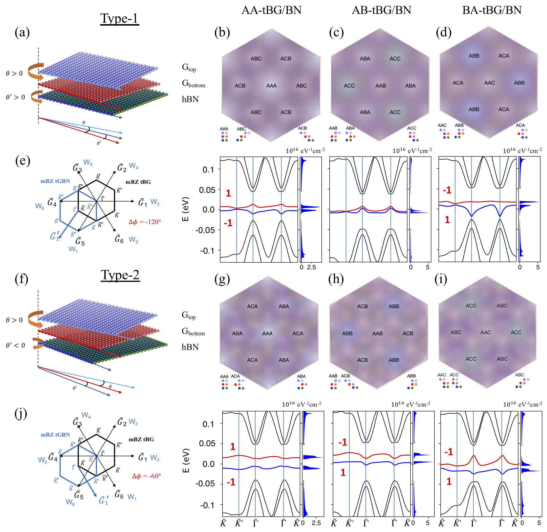
The model Hamiltonian for doubly commensurate tBG/BN can be conveniently formulated through the moire bands theory with a single Brillouin zone Bistritzer and MacDonald (2011); Jung et al. (2014) without needing to recourse to a supermoire framework for incommensurable double moire patterns Anđelković et al. (2020); Zhu et al. (2020b); Wang et al. (2019); Leconte and Jung (2020). The Hamiltonian matrix elements arising from the two moire interfaces from tBG and tGBN lead to two types of arrangements illustrated in Fig. 1(a)(f) that can be built by properly matching the orientation of the moire pattern angles with the moire reciprocal lattice vectors, see Fig. 1(e)(j). The continuum model Hamiltonian is concisely given as , where is the Hamiltonian of tBG for the valley
| (1) |
where = diag(, , , ) represents the interlayer potential difference resulting from an applied electric field in the perpendicular direction, and describes the moire potential corresponding to BN placed underneath tBG, where represents a Dirac Hamiltonian for the bottom (b) and the top (t) layers of tBG rotated by (: counterclockwise, : clockwise), yielding
| (2) |
where and the Fermi velocity is , choosing eV Chebrolu et al. (2019). Here, , and is the -component of Pauli matrix. The interlayer coupling is given by
| (3) |
where , are given as , if the twist angle is small enough. Here, is the magnitude of graphene Brillouin zone (BZ) corner wavevector where the lattice constant of graphene is given as . The interlayer tunneling matrices were formulated for the AA initial stacking in Ref. Jung et al., 2014 as
| (4) |
where and and describes a relative sliding of the top G layer with respect to the bottom layer of graphene, and , and , we get
| (5) |
for local AA-stacking corresponding to , where . The local AB-stacking corresponds to , and the local BA-stacking is given by or, equivalently, . By taking different eV and eV for the intra- and inter-sublattice coupling between layers related through where , , and following the EXX+RPA total energy minima parametrization Chebrolu et al. (2019); Park et al. (2020).
For tBG/BN, the moire potential Hamiltonian has the form
| (6) |
where
| (7) |
Here, are the polar angles of six moire reciprocal lattice vectors of the tGBN interface with a prime symbol to distinguish from the unprimed moire reciprocal lattice vectors for tBG. Here we use the moire potential parameter set given by meV, , meV, , meV, following Refs. Jung et al., 2015, 2014.
For tBG, the reciprocal lattice vectors of BZ of graphene are , and the moire reciprocal lattice vectors are given by (). On the other hand, for tGBN we have . We assume that for the commensurate angle sets (see the next section for further details), the mBZ of tBG and tGBN have the same size and share their two corners in momentum-space as shown in Fig. 1 (e), (j) (see Appendix A for further details).
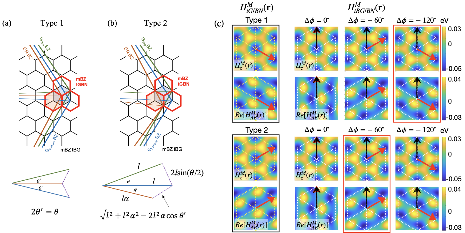
We label each commensurate stacking in real-space with three characters, A, B, and C to label from bottom to top layers the relative position of the left sublattice of the two atoms unit cell of G or BN. For instance, when the local AA-stacking region in tBG is AA stacked on top of hBN (AA-tBG/BN), a type-1 system gives rise to three AAA, ABC, and ACB local stacking at the symmetry points, while AAA, ACA, and ABA local stacking appear in type-2 systems. We plot each of the commensurate stacking configurations of tBG/BN with six small colored circles under the moire patterns for type-1 in Fig. 1 (b)-(d) and for type-2 in (g)-(i).
III commensurate twist angle sets
Among the many possible commensurate double moire patterns Leconte and Jung (2020); Anđelković et al. (2020); Wang et al. (2019) here we want to focus on the subset that can be obtained by requiring two constraints: (1) moire length: the moire lengths of tBG and tGBN should be the same, and (2) moire angle: the difference of moire angle should be 0 (mod ). The moire length of tBG is
| (8) |
and the moire length of tGBN is
| (9) |
where and Jung et al. (2014) are parameters that represent the lattice mismatch between two layers. We use for the lattice constant of graphene and boron nitride , which results in . Here, we use the notation for angles measured with respect to the bottom graphene (G) layer for convenience since both moire interfaces are sharing it; we define as the twist angle of tBG which is measured with respect to the bottom G layer and is the twist angle of BN measured with respect to the contacting bottom G layer at the tGBN interface and hence the minus sign. The condition for coincident moire lengths requires the following relation between and
| (10) |
Accordingly, the rotation angle of the moire pattern in tBG with respect to the bottom G layer is Jung et al. (2014)
| (11) |
This expression reduces to
| (12) |
indicating that the moire pattern orientation rotates with respect to the bottom G by one half of the total twist angle between the graphene layers. On the other hand, the tGBN moire pattern rotation angle measured with respect to the bottom G layer is given by
| (13) |
The condition for the two equal period moire patterns to be commensurate is
| (14) |
where is an integer number Leconte and Jung (2020). There is no analytical solution for but we have for the type-1 solution at or equivalently, because of periodicity of the tangent function, and have for the type-2 solution at or equivalently . The rotation of the moire patterns and associated moire Brillouin zones are shown graphically in Fig. 1 (a), (f) in real-space and Fig. 1 (e), (j), and Fig. A1 in appendix A in momentum space. The main differences between the two solutions are that in type-1 systems the top G layer and bottom hBN layer are rotated in the same sense , ) with respect to the bottom G layer, while in type-2 they are rotated in the opposite directions with respect to the bottom G layer , ). Imposing equal moire length conditions from Eqs. (8,9) leads to
| (15) |
that is equivalent to Eq. (14) with when we use the relation Cea et al. (2020); Shi et al. (2020) reducing to
| (16) |
that yields same sign angles for type-1 solutions , . The equations for unequal sign angles for type-2 solutions can be formulated by combining both Eqs. (14,15) for and their numerical solutions are , . Geometric discussions of the double moire commensuration conditions in real and momentum space are discussed in Appendix A. The real-space moire patterns of the commensurate double moire patterns for the three different stackings configurations between the top and bottom G layers for both type-1 in Fig. 1 (b-d) and type-2 systems are shown in Fig. 1 (g-i) where we can clearly see their differences both in the real-space patterns as well as in their momentum space band structures.
IV Band structures
In this section we present the band structures of tBG/BN corresponding to the two types of commensurate stacking arrangements introduced in earlier sections as a function of moire pattern sliding and perpendicular external fields. We will be paying attention to the bandwidth, gaps, and electron-hole asymmetry. Knowledge of the band structure allows to estimate regimes of strong correlations that satisfy where the bandwidths are sufficiently narrow versus the effective Coulomb interaction
| (17) |
where we used the dielectric constant of graphene as , the moire length and the screening length that depends on the two-dimensional density of states defined in terms of the Heaviside step function that includes screening due to overlap between neighboring bands. Chebrolu et al. (2019) The valley Chern number of the energy band is obtained integrating the Berry curvature Xiao et al. (2010) given by . Additional information on the electronic structure can be found in appendix C where we present the normalized local density of states (LDOS) whose maxima are expected at the AA stacking sites of tBG.
IV.1 Type-1 and type-2 electronic structures
We can distinguish two arrangements of double moire patterns that we classify as type-1 and type-2 depending on the relative twist of the layers in the tBG and tGBN substrate that in turn impacts the relative rotation of the associated moire patterns . For double moire patterns of type-1 we require a relative rotation of or equivalently between the mBZ of tBG and tGBN as shown in Fig. 1(e). On the other hand, for type-2 we require (see Appendix A) or equivalently as shown in Fig. 1(j). The impact in the band structure of tBG/BN is represented along the high-symmetry line of mBZ of tBG (), we show the band structures for in Fig. 1(b-d) for type-1 and in Fig. 1 (g-i) for type-2 for different displacement of the top G layer for an electronic structure model with unequal interlayer tunneling value that incorporates an effective vertical relaxation Chebrolu et al. (2019); Park et al. (2020). In our analysis the twist angles of tBG compatible with the double commensuration defined by Eqs. (13)-(14) essentially depends on the value of the lattice constant mismatch . The double commensuration angles and result from our choice of graphene and BN lattice constants. We can expect the bandwidths will remain narrow provided that these angles remain close to the experimental Cao et al. (2020) and theoretical Bistritzer and MacDonald (2011); Chebrolu et al. (2019); Park et al. (2020) values where flat bands emerge. We estimated the changes in the electronic structure for twist angles of tBG away from the magic angle by using an approximation scheme that preserves commensuration with the hBN moire pattern potential which shows a similar qualitative behavior in the vicinity of the magic twist angle for variations on the order of or smaller, see appendix C Fig. A3.
The electronic structures depend strongly on the relative sliding between the moire patterns of tBG and tGBN. We use a vector to indicate the sliding of the top G layer prior to rotation and with this notation the local AA-, AB-, and BA-stackings at the origin correspond to , , and . The local stacking maps between the two graphene sheets and BN subsrate are traced by assuming that the BN substrate is locked at the AA stacking configuration with respect to the bottom graphene layer. For instance, the AA-tBG/BN case where tBG is AA stacked prior to twisting corresponds to Fig. 1(b) and (g). For type-1 we can find a small gap of meV at while for type-2 the lowest energy bands are quasi-flat with a large gap of meV at and meV at . For AB-tBG/BN corresponding to Fig. 1(c) and (h), type-1 bands consist of mutually overlapping bands with large secondary gaps for both conduction and valence bands that separate the lowest energy bands with the next band that is farther in energy from charge neutrality, whereas for type-2 we find isolated low energy conduction and valence bands with a gap of size meV at . For BA-tBG/BN corresponding to Fig. 1 (d), we see a large electron-hole asymmetric electronic structure separated with a small primary gap meV consisting of a nearly flat low energy conduction band with meV and wider valence band meV that reminds of the experimental observations of spontaneous Hall effects for electrons but not for holes Sharpe et al. (2019); Saito et al. (2020). Conversely for type-2 we have wider conduction and narrower valence bands that are separated by a finite gap of meV for the entire mBZ.
For both types of solutions, the secondary gap for the conduction and valence bands remain open for the three AA, AB, BA symmetric stacking geometries, and we will show shortly that this is the case for the entire range of sliding geometries. This is in contrast to the behavior of the primary gap that clearly closes when the top G layer is placed at in a type-1 system.
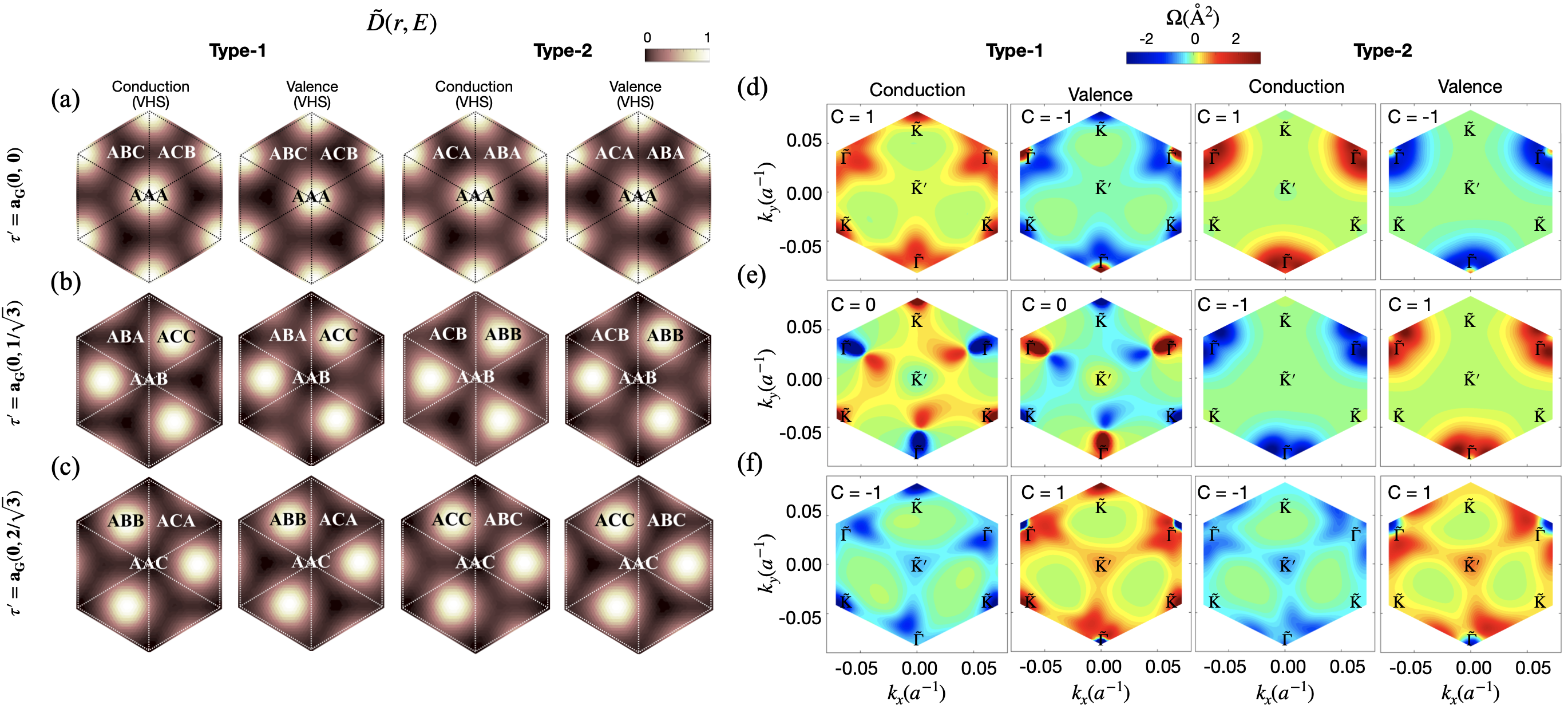
The Berry curvatures for discrete three commensurate slidings of the top G layer for conduction and valence band and the normalized local density of states at the van Hove singularity (vHs) can be found in appendix C Fig. A4 that illustrates the impact of the BN substrate in altering those quantities.
Having identified the distinct behavior of the bands for type-1 and type-2 moire pattern arrangements at three different symmetric stacking configurations we discuss in the following the dependence of the band structure to other continuous stacking sliding geometries and interlayer potential differences.
IV.2 Sliding and electric field dependent electronic structure
Here we extend our analysis of the lowest energy bands to other continuous stacking geometries as a function of and explore the changes in the electronic structure due to an interlayer potential difference introduced by a perpendicular electric field.
| Type-1 | Type-2 | |||
|---|---|---|---|---|
| (meV) | ||||
| 15.2 | 29.2 | 26.5 | 21.7 | |
| 6.0 | 6.0 | 8.2 | 8.9 | |
| 11.6 | 13.1 | 15.0 | 14.8 | |
| 1.9 | 4.6 | 4.8 | 2.6 | |
For all possible local stacking geometries we have obtained the maxima, minima, average and the standard deviations of the bandwidths, which we succinctly summarize in Table 1. From this data we can observe a more pronounced electron-hole asymmetry for type-1 systems with narrower conduction bands on average and smaller bandwidth fluctuations that posits the preference of the conduction bands to form ordered phases with respect to the valence bands. On the other hand, we expect a higher likelihood of observing ordered phases for both conduction and valence bands for type-2 systems because the electron-hole asymmetry is generally less pronounced, while narrower valence bands with smaller fluctuations are found for the average results.
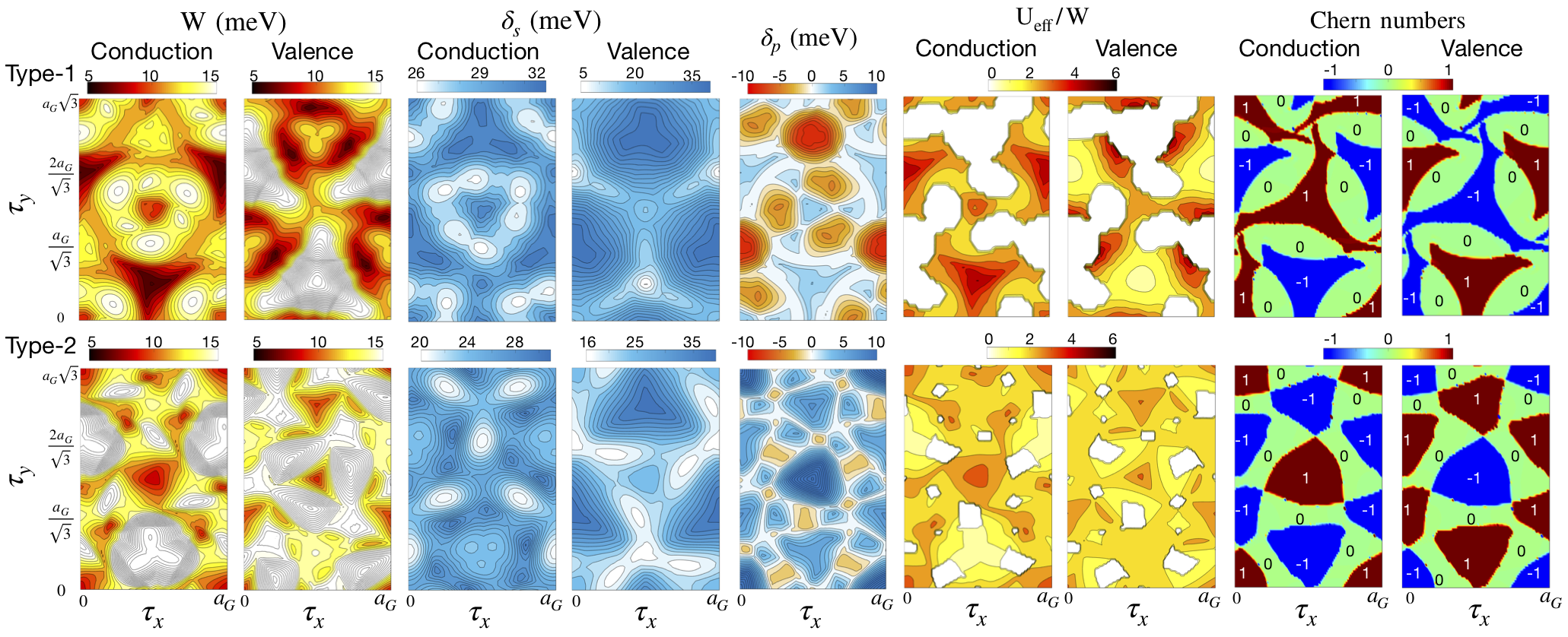
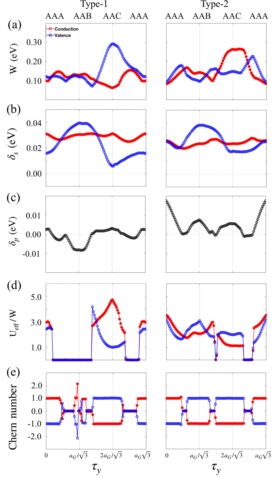
The phase diagram maps for the bandwidth , the ratios, the gaps, and valley Chern number maps for continuous stacking geometries are shown in Fig. 2. The stacking configurations with the narrowest bandwidth and largest gaps have greater chances of enhanced Coulomb interactions that can lead to ordered phases. For roughly half of the stacking configuration space we can observe favorable condition and they largely coincide with the regions that have finite valued valley Chern numbers. The regions with suppressed are mainly due to the closure of the primary gap that overlaps the two low energy flat bands and enhances the Coulomb screening.
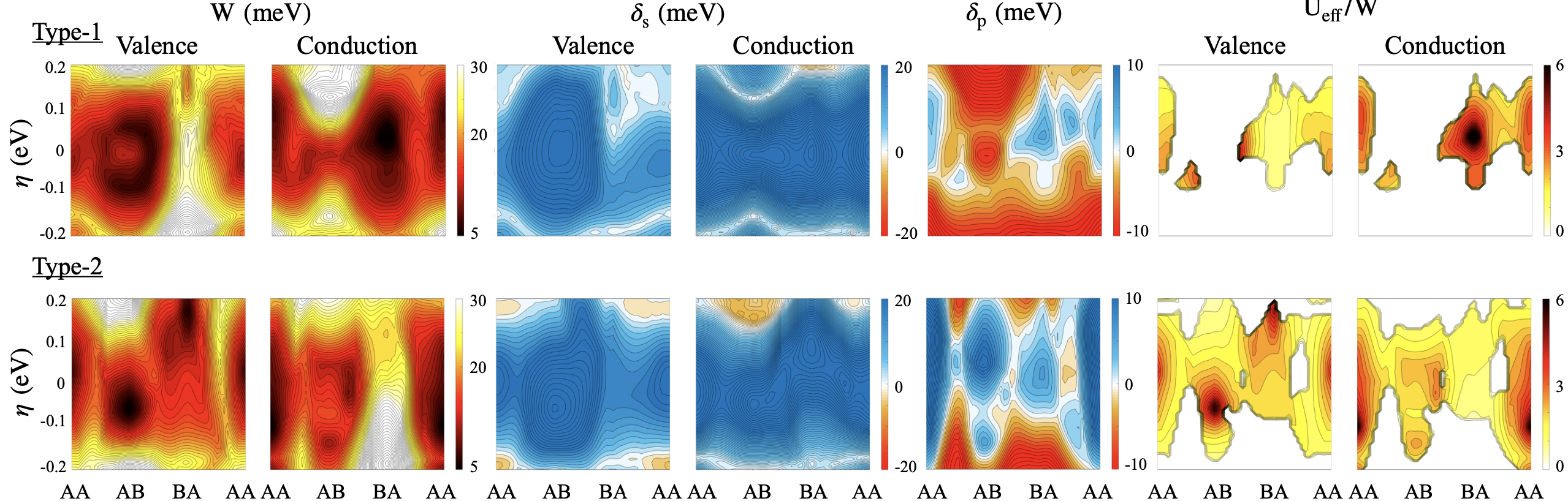
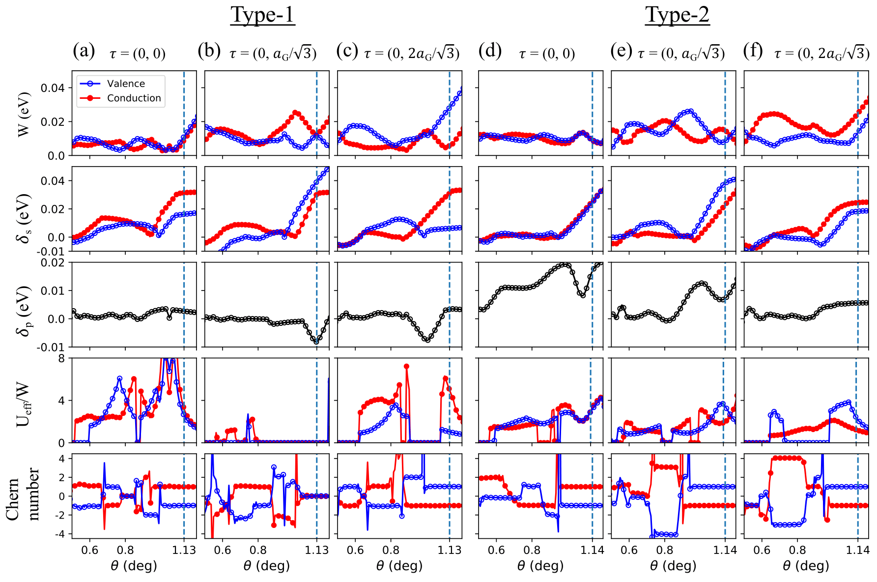
The phase diagram maps for the bandwidth , the gaps and resulting ratios in Fig. 3 shows that a perpendicular electric field directed in the appropriate sense can enhance the narrowing of the bands and has an overall effect of enhancing the secondary gap , while the opening and closure of the primary gap follows a more complex behavior as a function of stacking and applied electric fields.
IV.3 Band gap analysis at point
As discussed earlier, distinct electronic low energy bands are expected depending on the moire pattern stacking types that we classify as type-1 and type-2. For example, in type-1 of AA-tBG/BN there is a small gap meV at in contrast to the large gap meV in type-2. A band gap near charge neutrality in tBG/BN double moire systems can be expected to appear due to moire pattern interference effects. We illustrate this behavior by obtaining the analytical expressions for the size of the gaps at for different moire pattern types and relative stackings arrangements as a function of the model parameters that define the moire patterns. For this purpose we consider a truncated Hamiltonian as a simple model to describe tBG system that captures the scattering of the electrons from the three Dirac cones of the bottom layer to one Dirac cone on the top layer Bistritzer and MacDonald (2011). At the eigenstates can be represented by consisting of four two-component sublattice pseudospin spinors Javvaji et al. (2020). Here the , spinors can be rewritten in terms of by multiplying with a unitary matrix and , and thus allowing to further reduce our Hamiltonian to a 33 matrix to obtain a simpler characteristic equation. Then, the expression for the band gap at is,
| (18) |
where . This expression agrees up to 2 significant digits with the gap size obtained by diagonalizing numerically the eight-band model. The above equation holds for both type-1 and type-2 solutions and for the three symmetric AA, AB, BA stackings but the analytical coefficients and are different for each case. Below we present the expression for the and coefficients for type-1 BA-tBG/BN for the electronic structure showing the largest electron-hole asymmetry that incorporates the effect of the interlayer potential difference that can be induced by a perpendicular electric field and the moire pattern potentials generated by the BN substrate that affects the magnitude of the gap. For sufficiently small magnitudes of the and coefficients in Eq. 18 can be expressed in terms of the moire pattern coefficients stemming from the hBN substrate as follows
and
In Appendix B we show a more detailed derivation of the analytic expressions for other types of solutions and stackings.
V Optical conductivity
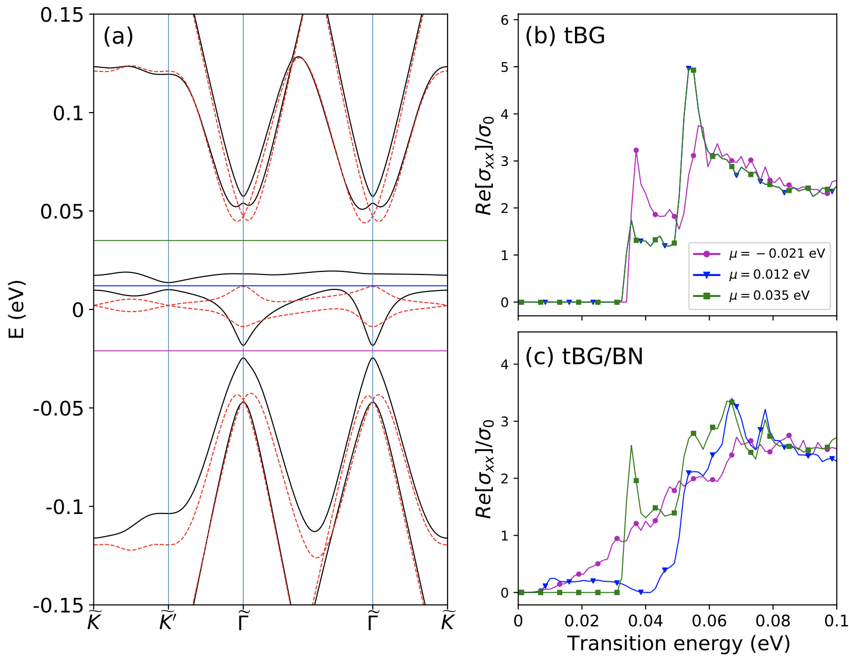
Electronic structure reconstruction in the energy ranges of a few tens of meV in the vicinity of the Dirac cone of graphene can be conveniently explored by means of mid-infrared and terahertz spectroscopy. Here we show the numerical results for the optical absorption in type-1 BA-tBG/BN as well as tBG without a BN substrate in an effort to estimate the differences in the optical signals that can be expected in these two systems. The real part of the longitudinal optical conductivity normalized by the universal optical conductivity of graphene is given by Ando et al. (2002); Gusynin et al. (2006, 2007); Falkovsky and Varlamov (2007); Min and MacDonald (2009)
| (21) |
where is the current operator, is the Fermi-Dirac distribution function. is the th eigenstate energy at . In Fig. 4(a) we show the energy bands for type-1 BA-tBG/BN (black solid line) and tBG (red dotted line) without a BN substrate where we achieve double commensuration of equal period moire patterns by using the twist angles of (, ) = (1.13291∘, 0.5664∘) as we introduced earlier. The horizontal lines are the three different chemical potentials (magenta circle), 0.012 (blue triangle), and 0.035 eV (green square) considered, and we plot the real part of the linear optical absorption in the longitudinal direction for tBG in Fig. 4(b) and type-1 BA-tBG/BN in Fig. 4(c). The presence of the BN substrate leads to markedly different asymmetric optical absorptions for eV (magenta circle) and eV(green square), and one can observe small gaps less than 10 meV for eV (magenta circle), eV (blue triangle) in type-1 BA-tBG/BN as shown in Fig. 4(c), unlike without BN.
| = | ||||||||
|---|---|---|---|---|---|---|---|---|
| type-1 | 0.284447 | 0.379079 | 0.568072 | 1.132910 | 2.253321 | 3.362061 | 4.459900 | |
| 0.576353 | 0.575245 | 0.573035 | 0.566455 | 0.553515 | 0.540851 | 0.528445 | ||
| type-2 | 0.285284 | 0.380567 | 0.571420 | 1.146307 | 2.306986 | 3.483098 | 4.675807 | |
VI Commensurate double moire angle sets
So far we have considered doubly commensurate systems with equal moire pattern lengths and here we extend our band structure analysis to commensurate double moire systems with unequal individual moire lengths. An example of a doubly commensurate supermoire built from unequal length moire patterns was realized in twisted double bilayer graphene on hexagonal boron nitride arranged in a way that it gives rise to a Kekule-type supermoire lattice whose moire bands are flattened and isolated Lee et al. (2020). We expect that a similar bandwidth narrowing and band isolation behavior due to zone folding and formation of avoided gaps could take place in tBG/BN systems. Here we explore the band structures of supermoire systems formed by combining unequal individual moire lengths that are multiples of each other and have modulo 60∘ alignment. The Hamiltonian matrix elements of the commensurate double moire pattern can be built from the matrix elements of each moire pattern labeled by the respective moire reciprocal lattice vectors whose magnitude and relative orientations will change depending on the twist angle sets considered.
Our analysis focuses on the cases when the moire lengths of tBG are greater than those of tBG for and ratios considering that the moire length for tBG and for tGBN as a function of twist angles , are given in Eq. (8) and (9). These commensurate supermoire patterns can be achieved in the limit of small tBG twist angles and gives rise to zone folding as the moire Brillouin zone reduces in size. The set of twist angles that satisfy the commensuration conditions are listed in Table 2 for type-1 and type-2 systems when = for some integer and rational values of .
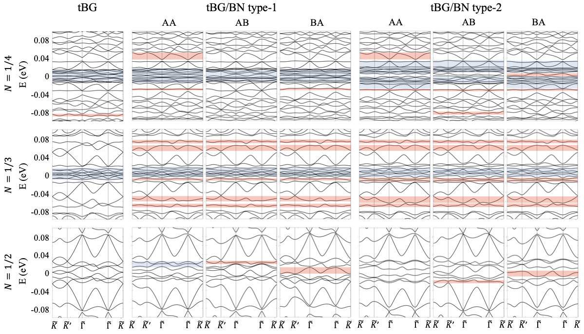
The resulting band structures are presented in Fig. 5 for the three different starting stackings, AA, AB, and BA where we can observe bundles of narrow bands that we highlight with blue-shades that are separated from each other forming bands of moire bands. Likewise we have also highlighted with red shades the isolated nearly flat moire bands that are separated from each other through avoided gaps. In particular we find that the band bundles for , commensurate ratios can have bandwidths of the order of meV.
These folded nearly flat bands are weakly dispersive in the reduced moire Brillouin zones in the limit of small tBG twist angles. We expect that the moire pattern features that appear at low energies due to the BN substrate can introduce gaps that separate the folded band bundles that enhance their isolation and reduce their screening. The notable changes in the band structures that we can observe for different relative sliding configurations for the doubly commensurate geometries indicate that small deviations of the twist angles can in principle lead to significant changes to the electronic structures, while we might also expect formation of gaps between the folded moire band bundles due to the BN substrate. As we approach the regime of marginally twisted graphene bilayers we expect that the commensuration strain effects will become more important and should be considered in a more complete theory.
VII conclusion
We have investigated the electronic structure of commensurate double moire patterns of twisted bilayer graphene (tBG) on hexagonal boron nitride (BN) in an effort to understand the effects introduced by a BN substrate when it is brought to near alignment with the graphene layers, and identify the conditions that are favorable for the appearance of gapped moire bands with finite valley Chern numbers that ultimately lead to the anomalous Hall effects observed in experiments.
The band structure of tBG has been calculated based on a continuum model that effectively accounts for vertical interlayer relaxations by using unequal interlayer tunneling parameters. The effects of a second moire pattern produced by the BN substrate have been modeled assuming a moire pattern that is perfectly commensurate with tBG which conveniently allows us to study the physics of the system based on a single moire Brillouin zone continuum Hamiltonian model. For these doubly commensurate geometries we have highlighted the importance of aligning properly the moire reciprocal lattice upon rotation to properly construct the continuum moire Hamiltonian, and have illustrated the role of the BN moire patterns and interlayer potential differences in opening the primary band gaps by obtaining the analytical form of the gaps near for a truncated model.
When the periods of each moire patterns are equal, we have identified two types of commensurate double moire patterns depending on the relative twist angles of the tBG layers with respect to the BN substrate that we classified as type-1 and type-2 and whose band structures have revealed markedly different features in their electron-hole asymmetry, the formation of band gaps, and dependence on local interlayer sliding arrangement. In type-1 double moire systems we find narrower overall conduction bands than valence bands with the most prominent asymmetry appearing in the vicinity of the BA-tBG/BN stacking configuration where the conduction band has the smallest bandwidth meV suggesting that conduction bands are more prone for broken symmetry phases than the valence bands, whereas the electron-hole symmetry is partially restored in type-2 solutions that slightly favor on average the narrowing of the valence bands suggesting that ordered phases will likely appear for both conduction and valence bands. The impact of the BN substrate on the electronic structure should be observable not only through transport measurement but also through the optical absorption probes as we illustrated for the specific BA-tBG/BN example versus tBG without a substrate.
We have extended our electronic structure study to other commensurate double moire systems with unequal moire pattern lengths focusing on the smaller bilayer graphene twist angles and verified that they often lead to separated folded moire bands bundles with reduced widths meV. Hence, our results suggest that tBG twist angles in the range of clearly below can also be candidate systems for exhibiting correlated phases.
The analysis presented in this work for commensurate double moire patterns for a variety of different sliding geometries shows how the BN substrate impacts the electronic structre of tBG, specifically leading to band gap openings that isolate the moire bands. Additionally, these band structures provide a useful starting point for understanding the electronic structure of incommensurate double moire tBG/BN systems that can be pictured as a coherent combination of the commensurate states with different stacking. A more detailed study of the incommensurate double moire patterns as they depart from perfect commensuration as well as the impact of lattice relaxations in the electronic structure is desirable to understand in greater detail the precursor states leading to the experimentally observed anomalous Hall orbital magnetization in tBG/BN.
VIII acknowledgments
We gratefully acknowledge discussions with J. H. Sun for the derivation of the analytic band gaps. This work was supported by Samsung Science and Technology Foundation under project no. SSTF-BA1802-06 for J. S., the Korean National Research Foundation (NRF) grant NRF-2020R1A5A1016518 for Y. P., the Basic Science Research Program of the NRF-2018R1A6A1A06024977 for B. L. C., and by grant NRF- 2020R1A2C3009142 for J. J. We acknowledge computational support from KISTI through grant KSC-2020-CRE-0072.
Appendix A: Geometrical derivation of commensurate twist angles and moire pattern rotations
There are two classes of solutions for moire lengh commensurate tBG/BN as shown in Fig. 1. Here we present a geometrical proof for both types of solution in momentum-space and a more detailed analysis about how type-1 and type-2 moire potentials in real-space lead to relative moire pattern rotation angles of and respectively.
We assume that the bottom G and top G layers are rotated by and , respectively. In Fig. A1 we plot the BZ of the bottom G layer with a thick blue solid line and the BZ of the top G layer with a thick green solid line, generating the mBZ of tBG which plotted by a black thin solid line. The thick brown solid line represents BZ of hBN. For tBG/BN to be commensurate, mBZ of tBG and of tGBN should have the same size and share their two corners. The geometrical understanding for type-1 is straightforward since the simple relation holds as shown in Fig. A1(a). For type-2, on the other hand, if we assume the length from the center to the corner of BZ of hBN layer is , then the length from the center to the corner of BZ of G layer is , and the two lengths indicated by the dashed purple line in Fig. A1 must be the same to share the two corners of the mBZ of tBG and tGBN. Then we get an equation which is equivalent to condition in Eq. (10). The shaded areas in red and blue in the upper row in Fig. A1(a) and (b) correspond to the mBZ depicted in Fig. 1(e) and (j), respectively.
We now move on to discuss the rotation of the moire patterns. The moire potential in Eq. (6) can be rewritten for the bottom G layer with a 22 matrix as follows
| (A1) |
where are the moire reciprocal vectors of tGBN
| (A2) |
| (A3) |
and
| (A4) |
Here, and is the magnitude of the moire reciprocal lattice vector of tBG. In the pseudospin basis represents the periodic moire potential, and is the local mass term that can gives a gap at the neutrality point. The is a non-Abelian SU(2) gauge potential in the in-plane direction due to the unequal in the hopping probability between different sublattices of a honeycomb lattice Vozmediano et al. (2010); Jung et al. (2017). We can rewrite the term as where is , and then from the real space maps of the rotated moire potentials and we can verify the correct alignment required for the moire reciprocal lattice vectors of both interfaces to assign the moire pattern coefficients in the Hamiltonian matrix.
The leftmost column of Fig. A1 (c) shows the mass term in real-space and the real part of gauge field of tGBN and the red arrows represent the one of moire lattice vectors resulted from the moire patterns. On the other hand, the right three columns gives and of tBG/BN for different . The black arrows are the moire lattice vector directions of tBG and the red arrows are those of tBG/BN. Note in Fig. A1 (c) that the two components of the moire potential, and in real-space for tGBN are in agreement with those of tBG/BN when for the case of type-1 (type-2) as also illustrated in more detail in Fig. 1 (e), (j).
Appendix B: Band gap analysis at
Here derive the analytic expressions for the energy gap at a specific high-symmetry point that often is a useful estimate of the actual band gap at charge neutrality. We first consider truncating the range of -vectors for an eight-bands model of tBG Bistritzer and MacDonald (2011) possessing three Dirac Hamiltonians for the bottom layer and one Dirac Hamiltonian for the top layer. We use the fact that among the four two-component pseudospin eigenstates in the basis , Javvaji et al. (2020) the two spinors and can be written at in terms of by a unitary transformation as follows, for example, for AA-tBG/BN
| (A5) |
for conduction (valence) band in type-1 (type-2), and
| (A6) |
for valence (conduction) band in type-1 (type-2), we reduced our 88 Hamiltonian into 33 matrix to find a secular equation. In type-1 for the conduction band,
| (A7) |
and for the valence band,
| (A8) |
where the eigenstates of the conduction and valence band for eight-band model are given as and . Here, .
We get characteristic equations from the above matrices. For example,
| (A9) |
and
| (A10) |
where
| (A11) |
and
| (A12) |
for (type-1) and (type-2). For type-1, and in the order of AA-, AB-, BA-tBG/BN are given as follows.
| (A13) |
| (A14) |
| (A15) |
| (A16) |
Also, and are given as follows, for type-1 AA-tBG/BN,
| (A17) |
| (A18) |
for type-1 AB-tBG/BN,
| (A19) |
and
| (A20) |
and for type-1 BA-tBG/BN,
| (A21) |
and
| (A22) |
Since and are negligibly small, we can get three roots for each, , , and , , presuming . By retrieving , and plugging the lowest energies , , whose eigenvectors remain the same, into the original characteristic equations, we get a much more simplified expressions for the energy gap as written in Eq. (18). In the same manner, for other stackings of tBG the characteristic equations have the same form but the coefficients are different since the unitary matrix connecting the spinor bases are different, resulting in different characteristic equations.
For AA-tBG/BN of type-2, the matrix for a characteristic equation is given as
| (A23) |
| (A24) |
where the eigenstates of the conduction and valence band for eight-bands model are given as and . This matrix gives us two equations, Eq. (A9) and Eq. (A10), as in type-1. The constants , , , also follow the same equations Eq. (A11) and Eq. (A12) with different and as follows.
| (A25) |
| (A26) |
| (A27) |
| (A28) |
The and parameters for type-2 systems are given by
| (A29) |
| (A30) |
for AA-tBG/BN,
| (A31) |
| (A32) |
for AB-tBG/BN and
| (A33) |
| (A34) |
for BA-tBN/BN.
The analytical values of the gaps in the presence of an interlayer potential difference will be shown only for the case of BA-tBG/BN in type-1. The associated matrix for the characteristic equation is
| (A35) |
for conduction band, and
| (A36) |
for the valence band, where the eigenstates of the conduction and valence bands in the eight-bands model are given as and . This expressions is the same as Eq. (18) for the gap at but using with different coefficients.
Appendix C: supplemental electronic structure, local density of states and Berry curvatures
Here we supplement information on electronic structure presented in the main text for the bandwidth , the secondary band gaps , primary band gaps , the ratio of the screened Coulomb interaction strength to the bandwidth , and valley Chern numbers by considering the effects of twist angles under the assumptions of commensurate double moire patterns and also provide information of the local density of states at the van Hove singularities and the Berry curvatures of the nearly flat bands.
We begin by presenting in Fig. A2 through 1D plots various electronic structure information for variable and fixed that had been discussed in the main text. The topmost row (a) panel shows the fluctuations in the bandwidth for the low energy conduction and valence bands as a function of where we can find a relatively narrower conduction band versus valence band for type-1 systems and more electron-hole symmetric bands for type-2 systems. Subsequent rows represent (b) the secondary band gaps and (c) the primary band gaps. Information from (a)-(c) panels are used to determine (d) the ratio where we can clearly observe its relative enhancement for conduction bands in type-1 but maintaining comparable magnitudes for electrons and holes for type-2 systems. The valley Chern numbers in (e) showing well quantized values or oscillating with non-integer values as a function of are in keeping with the fact that the bands are isolated when we have positive primary and secondary gaps.
In Fig. A3 we provide additional information about how the electronic structure will be modified when we allow the twist angle of tBG to change from the specific values determined by the double moire commensuration condition. For this purpose we make the approximation that double commensuration is maintained for every value of which implies that the moire pattern period and angle also change continuously together with the pattern of tBG. The dashed vertical line indicates the commensuration angle for tBG consistent with the lattice constants of graphene and hexagonal boron nitride . We may expect that the double commensuration condition can still hold approximately in the vicinity of this vertical dashed line thanks to lattice relaxation effects that rotate and globally relax the lattices. The information in Fig. A3 allows to distinguish the expected electronic structures features in the lowest energy conduction and valence bands for different initial interlayer sliding stacking geometries AA-tBG/BN [], AB-tBG/BN [], and BA-tBG/BN [] prior to rotation. While the relative sliding of the layers are shown to considerably modify the low energy electronic structure, as we illustrate in Fig. A4 through normalized local density of states (LDOS) we also find that the electron localization largely concentrates at the AA stacking sites of tBG regardless of the arrangement of the BN substrate. Quantitative differences in the normalized LDOS are still expected to be observable near AB or BA local stacking regions when relative sliding between layers are introduced. Likewise the Berry curvature maps undergo changes in their hotspot distributions depending on which stacking configuration is chosen. These differences could impact the Hall transport and optical measurements especially when valley contrasting circularly polarized light is used.
References
- Cao et al. (2018a) Y. Cao, V. Fatemi, S. Fang, K. Watanabe, T. Taniguchi, E. Kaxiras, and P. Jarillo-Herrero, Nature 556, 43 (2018a).
- Cao et al. (2018b) Y. Cao, V. Fatemi, A. Demir, S. Fang, S. L. Tomarken, J. Y. Luo, J. D. Sanchez-Yamagishi, K. Watanabe, T. Taniguchi, E. Kaxiras, et al., Nature 556, 80 (2018b).
- Kim et al. (2017) K. Kim, A. DaSilva, S. Huang, B. Fallahazad, S. Larentis, T. Taniguchi, K. Watanabe, B. J. LeRoy, A. H. MacDonald, and E. Tutuc, PNAS 114, 3364 (2017) .
- Shi et al. (2020) J. Shi, J. Zhu, and A. H. MacDonald, arXiv preprint arXiv:2011.11895 (2020).
- Yankowitz et al. (2019) M. Yankowitz, S. Chen, H. Polshyn, Y. Zhang, K. Watanabe, T. Taniguchi, D. Graf, A. F. Young, and C. R. Dean, Science 363, 1059 (2019).
- MacDonald (2019) A. H. MacDonald, Physics 12, 12 (2019).
- Saito et al. (2020) Y. Saito, J. Ge, K. Watanabe, T. Taniguchi, and A. F. Young, Nature Physics 16, 926 (2020).
- Zhang et al. (2019a) Y.-H. Zhang, D. Mao, Y. Cao, P. Jarillo-Herrero, and T. Senthil, Phys. Rev. B 99, 075127 (2019a).
- Chittari et al. (2019) B. L. Chittari, G. Chen, Y. Zhang, F. Wang, and J. Jung, Phys. Rev. Lett. 122, 016401 (2019).
- Sharpe et al. (2019) A. L. Sharpe, E. J. Fox, A. W. Barnard, J. Finney, K. Watanabe, T. Taniguchi, M. A. Kastner, and D. Goldhaber-Gordon, Science 365, 605 (2019) .
- Lu et al. (2019) X. Lu, P. Stepanov, W. Yang, M. Xie, M. A. Aamir, I. Das, C. Urgell, K. Watanabe, T. Taniguchi, G. Zhang, et al., Nature 574, 653 (2019).
- Serlin et al. (2020) M. Serlin, C. Tschirhart, H. Polshyn, Y. Zhang, J. Zhu, K. Watanabe, T. Taniguchi, L. Balents, and A. Young, Science 367, 900 (2020).
- Haldane (1988) F. D. M. Haldane, Phys. Rev. Lett. 61, 2015 (1988).
- Bultinck et al. (2020) N. Bultinck, S. Chatterjee, and M. P. Zaletel, Phys. Rev. Lett. 124, 166601 (2020).
- Zhang et al. (2019b) Y.-H. Zhang, D. Mao, and T. Senthil, Phys. Rev. Research 1, 033126 (2019b).
- Tschirhart et al. (2020) C. Tschirhart, M. Serlin, H. Polshyn, A. Shragai, Z. Xia, J. Zhu, Y. Zhang, K. Watanabe, T. Taniguchi, M. Huber, et al., arXiv preprint arXiv:2006.08053 (2020).
- Polshyn et al. (2020) H. Polshyn, J. Zhu, M. Kumar, Y. Zhang, F. Yang, C. Tschirhart, M. Serlin, K. Watanabe, T. Taniguchi, A. H. MacDonald, et al., Nature (2020), https://doi.org/10.1038/s41586-020-2963-8 .
- He et al. (2020) W.-Y. He, D. Goldhaber-Gordon, and K. T. Law, Nature communications 11, 1650 (2020).
- Leconte and Jung (2020) N. Leconte and J. Jung, 2D Materials 7, 031005 (2020).
- Anđelković et al. (2020) M. Anđelković, S. P. Milovanović, L. Covaci, and F. M. Peeters, Nano Letters 20, 979 (2020).
- Wang et al. (2019) Z. Wang, Y. B. Wang, J. Yin, E. Tóvári, Y. Yang, L. Lin, M. Holwill, J. Birkbeck, D. J. Perello, S. Xu, J. Zultak, R. V. Gorbachev, A. V. Kretinin, T. Taniguchi, K. Watanabe, S. V. Morozov, M. Anđelković, S. P. Milovanović, L. Covaci, F. M. Peeters, A. Mishchenko, A. K. Geim, K. S. Novoselov, V. I. Fal’ko, A. Knothe, and C. R. Woods, Science Advances 5, eaay8897 (2019).
- Zhu et al. (2020a) Z. Zhu, S. Carr, D. Massatt, M. Luskin, and E. Kaxiras, Phys. Rev. Lett. 125, 116404 (2020).
- Cea et al. (2020) T. Cea, P. A. Pantaleón, and F. Guinea, Phys. Rev. B 102, 155136 (2020).
- Lin and Ni (2020) X. Lin and J. Ni, Physical Review B 102, 035441 (2020).
- Bistritzer and MacDonald (2011) R. Bistritzer and A. H. MacDonald, PNAS 108, 12233 (2011) .
- Jung et al. (2014) J. Jung, A. Raoux, Z. Qiao, and A. H. MacDonald, Physical Review B 89, 205414 (2014).
- Zhu et al. (2020b) Z. Zhu, P. Cazeaux, M. Luskin, and E. Kaxiras, Phys. Rev. B 101, 224107 (2020b).
- Chebrolu et al. (2019) N. R. Chebrolu, B. L. Chittari, and J. Jung, Phys. Rev. B 99, 235417 (2019).
- Park et al. (2020) Y. Park, B. L. Chittari, and J. Jung, Phys. Rev. B 102, 035411 (2020).
- Jung et al. (2015) J. Jung, A. M. DaSilva, A. H. MacDonald, and S. Adam, Nature Communications 6, 6308 (2015).
- Xiao et al. (2010) D. Xiao, M.-C. Chang, and Q. Niu, Rev. Mod. Phys. 82, 1959 (2010).
- Cao et al. (2020) Y. Cao, D. Rodan-Legrain, J. M. Park, F. N. Yuan, K. Watanabe, T. Taniguchi, R. M. Fernandes, L. Fu, and P. Jarillo-Herrero, arXiv preprint arXiv:2004.04148 (2020).
- Javvaji et al. (2020) S. Javvaji, J.-H. Sun, and J. Jung, Phys. Rev. B 101, 125411 (2020).
- Ando et al. (2002) T. Ando, Y. Zheng, and H. Suzuura, J. Phys. Soc. Jpn 71, 1318 (2002).
- Gusynin et al. (2006) V. Gusynin, S. Sharapov, and J. Carbotte, Phys. Rev. Lett. 96, 256802 (2006).
- Gusynin et al. (2007) V. Gusynin, S. Sharapov, and J. Carbotte, Phys. Rev. Lett. 98, 157402 (2007).
- Falkovsky and Varlamov (2007) L. Falkovsky and A. Varlamov, Eur. Phys. J. B 56, 281 (2007).
- Min and MacDonald (2009) H. Min and A. H. MacDonald, Phys. Rev. Lett. 103, 067402 (2009).
- Lee et al. (2020) K. Lee, M. I. B. Utama, S. Kahn, A. Samudrala, N. Leconte, B. Yang, S. Wang, K. Watanabe, T. Taniguchi, G. Zhang, A. Weber-Bargioni, M. Crommie, P. D. Ashby, J. Jung, F. Wang, and A. Zettl, arXiv:2006.04000 (2020) .
- Vozmediano et al. (2010) M. Vozmediano, M. Katsnelson, and F. Guinea, Physics Reports 496, 109 (2010).
- Jung et al. (2017) J. Jung, E. Laksono, A. M. DaSilva, A. H. MacDonald, M. Mucha-Kruczyński, and S. Adam, Phys. Rev. B 96, 085442 (2017).
- Shi et al. (2020) J. Shi, J. Zhu, and A. H. MacDonald, arXiv preprint arXiv:2011.11895 (2020).