Electron density effect on spin-orbit interaction in [001] GaAs quantum wells
Abstract
The spin-orbit interaction of two-dimensional (2D) electrons in semiconductor quantum wells gives rise to a varity of interesting transport and optical spin-dependent effects. In the GaAs/AlGaAs type heterosystems, this interaction consists of the isotropic Bychkov-Rashba term, which is absent in symmetric wells, and the anisotropic Dresselhaus term, reflecting the lattice symmetry. It is well-known that the first term can be controlled by electric fields in the growth direction: external or internal, induced by a charge density of 2D electrons. In this work we reveal that the 2D electron charge can substantially affect also the Dresselhaus interaction in symmetric quantum wells. Within the one-band electron Hamiltonian containing, together with the bulk Dresselhaus interaction, the two contributions to the Dresselhaus term from the quantum well interfaces, we show that the internal electric field from the 2D electron charge density can substantially renormalize the anisotropic spin-orbit interaction of 2D electrons. This effect may be important in quantitative studies of spin-dependent phenomena in quantum wells.
I Introduction
During the last three decades, extensive investigations of the spin-orbit interaction of two-dimensional (2D) electrons in the heterostructures based on the non-centrosymmetric cubic semiconductors were performed [1, 2, 3, 4]. For the bulk samples from these material the general form of the one-band effective mass electron Hamiltonian with the spin-orbit terms was established from a symmetry consideration [5, 6]. The magnitudes of these terms can be derived from the many-band Kane kp-models [6, 7, 8] or obtained in microscopic calculations [9, 10, 11, 12, 13, 14].
The spin-orbit interaction of 2D electrons in the heterostructures grown from the typical III-V semiconductors consists of the two parts with different symmetry: the Bychkov-Rashba term induced asymmetry of the structure in the growth direction and the Dresselhaus term related to the spin-orbit interaction in the crystal lattice.
In addition to the conventional bulk contribution to the anisotropic Dresselhaus interaction, there also exist the two anisotropic interface contributions, determined by the atomic structure of the interfaces of III-V semiconductors [15, 16, 14]. For qualitative explanation of the experiments on spin-dependent phenomena in 2D electron gas in quantum wells, both the bulk and the interface contributions are important (see for example Refs. [16],[17]).
The effect of the sharp interfaces on the states in the III-V semiconductor heterostructures is known since 1980s [18, 19, 20]. Corresponding interface anisotropic terms were introduced in the effective mass Hamiltonian for holes to explain the nature of the anisotropic exchange splitting of excitonic levels [21, 22]. Later, it has been noticed [23, 24] that the mixing of heavy and light holes at the interfaces also leads to a spin-orbit interface anisotropic term in the one-band electron Hamiltonian, being additional to the bulk Dresselhaus contribution. This term is one of the possible contributions to the interface anisotropic spin-orbit interaction of 2D electrons in III-V heterostructures, described within one-band Hamiltonian in Refs. [15, 16, 14]. In Refs. [11, 13, 14, 25] the parameters of the interface contributions were extracted from the tight-binding calculations of quantum wells grown in [110] and [001] directions. From the comparison, the values of the bulk and the interface parameters in the one-band electron Hamiltonian have been extracted. It was shown that the analytical one-band calculations perfectly reproduce the tight-binding numerical calculations for different quantum wells.
In this work we study the effect of the internal electrostatic field induced by the charge density of 2D electrons on the spin-orbit coupling of 2D electrons in symmetric [100] GaAs quantum wells. We use the one-band model [15, 16, 14] with account on the bulk as well as the interface terms in the effective electron spin-dependent Hamiltonian. We find the dependence of the spin splitting of the energy spectrum of 2D electrons on the electron density by solving the self-consistent system of the Schrodinger and the Poisson equations for the wave functions in a well. We show that the increase of the electron density substantially renormalizes the contributions from the bulk as well as the interfaces to the anisotropic part of the spin splitting of the 2D electron spectrum. A raise of the contribution from the interfaces to the Dresselhaus spin-orbit interaction stems from the pushing out of the electron wave function closer to the interfaces due to the Coulomb repulsion of electrons in the well. We conclude that the effect of change density on the spin splittings can be important in a precise determination of the magnitudes of the bulk and the interface spin-orbit parameters in GaAs type quantum wells.
II Structure design
First, we discuss the possible structure design and the realistic values of their parameters for which the effect of the 2D electron charge on the spin splittng of the energy spectrum is expected to be substantial.
We consider that the proper GaAs/AlGaAs heterostructures are similar to standard structures designed to obtain an ultra-high mobility 2D electron gas (2DEG). Let the barrier and the well layers be fabricated from the following typical compounds: Ga0.7Al0.3AsGaAsGa0.7Al0.3. To reach high electron densities in a quantum well (QW), the -doping is usually used. To avoid the Rashba effect, the heterostructure should be symmetric in the growth direction. The GaAs/AlGaAs heterosystems of this type were studied, for example, in Ref. [26]. Such structures are usually optimized to have the maximum mobility that implies that the doping layers are located far from the QW. However, in order to maximize the electron concentration of the 2DEG inside the QW, the doping layers should be as close to the QW as possible. Below we consider the structure design with the -doping layers located at the distance 20 nm from the QW, which still provides a sufficiently high mobility and a sufficiently large electron concentration [27].
It is natural to expect that the effect of the 2D electron charge on the spin splitting is large if the QWs are sufficiently wide. However, in wide QWs, if the 2D electron concentration is large, more than one electron subband can be populated. We do not discuss this case, as additional terms in spin-splitting electron Hamiltonian can appear due to the inter-subband mixing of spin-dependent wave functions(see e.g. [28, 29]). To determine the diapason of possible structure parameters when only lower subband is populated, we solve the system of the Poisson and the Schödinger equations for electrons in QWs at different QW widths. We increase the Fermi level and find the concentration when the lower electron subbands start to populate. For thin QWs, there exists a maximum electron concentration when Fermi level reaches the conduction band in the barriers. This maximum concentration strongly depends on the distance between QW and the -doping layers.
Results of solution of the system of the Poisson and the Schrödinger equations for the electron gas in quantum well as a function of QW width are shown in Fig. 1. The charge inside QW is compensated by the -doping which is modeled by the charge distributed in regions of the width of 2 Å at the distance of 20 nm from the QW boundaries. From Fig. 1 it is seen that the QW in this structure can not be populated above cm-2. We expect that in real structures this value is somewhat smaller because in our estimations we do not consider the details of doping (donor activation energy is neglected). When comparing with experimental values from standard high-mobility structures design [27], note that we assume symmetric -doping which doubles maximum possible density as compared with asymmetric -doping.
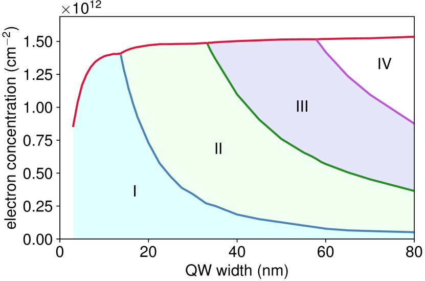
From Fig. 1 it is clear that the most favorable simple QW design for which the charge density inside the QW is maximal, being herewith distributed only in the first subband, corresponds to the QW width around 13 nm. However, it remains to be an open question whether the change of the electron density (relative to an almost empty well) at the points of the interfaces is maximal at the same QW width, 13 nm, or it is maximal for larger QWs.
III One-band Hamiltonian approach to spin splittings of 2D electrons
For quantum wells grown along the [001] direction from the zincblende semiconductors, the bulk spin-orbit term in the one-band electron Hamiltonian [8] has the form:
| (1) |
where is the bulk spin-orbit parameter, which depends on the layer material. In this formula we retained only the linear in the electron lateral wavevector contribution. The term (1) is anisotropic relative to rotations in the plane.
In quantum wells from zincblende semiconductors with abrupt interfaces, in addition to the bulk contribution (1), the anisotropic spin-orbit interaction also contains the interface contributions [24, 30, 31, 32, 15, 16, 17, 33]. They have the same symmetry as the bulk term (1), but are proportional, instead of the operator , to the delta-function and its derivative localized at the quantum well interfaces [16, 15]:
| (2) |
The parameters and are determined by the structure of the chemical bonds of the atoms on the interfaces. Equations (2) imply the continuity of the wave function derivative at the interfaces of the quantum well.
Comparison with the tight-binding calculations for Ga0.7Al0.3AsGaAsGa0.7Al0.3 quantum well gives the following values of the interface parameters and of the bulk cubic-in-k aplitting: eVÅ3, eVÅ2, eVÅ3, (see Ref. [14] for the details).
In the following, we consider a quantum well with a rectangular heteropotential . The function in this structure is a step-like function with the two different values in the well and in the barrier layers:
In the absence of an electric field , the symmetry of the quantum well is that leads to the relations between the coefficients and for the left and right interfaces: , .
The resulting anisotropic spin-orbit Dresselhaus Hamiltonian of 2D electrons containing the bulk and the interface contributions (1) and (2) and averaged by a wave function of a space-quantized level () is:
| (3) |
where the spin splitting parameter consist of the three contributions:
| (4) |
The potential energy of an electron in a rectangular quantum well with a substantial 2D electron charge density is:
| (5) |
where is the electrostatic potential induced by the 2D electron charge density. The potential is to be found from the solution of the Poisson equation:
| (6) |
Here we neglect the exchange contribution (see discussion in Ref. [16]). The density of charge corresponding to -doping is and the electron density is found from the electron wave functions taking into account the electron charge in the QW:
| (7) |
where -th subband electron density is:
| (8) |
and is the Heaviside step function. In Eq. (8) we neglect the finite temperature as we are interested in the case when the distance between electron levels is large as compared with the temperature. Electron wave functions are obtained from the numerical solution of Schödinger equation:
| (9) |
In real structures, the doping density is defined by the structure design and Fermi level is found from the system of equations (6,9) under electroneutrality condition . However, this approach involves finding roots of inexplicit non-linear equations. Technically, it is more convenient to construct the solutions for a set of structures with different 2D electron density starting from the structure with zero density and then increasing the Fermi energy in small steps. Then, the doping density is straightforwardly found from the electroneutrality condition and doping profile. Provided choosing a sufficiently small step in Fermi energy, all the values (the energies, the wave functions, and the spin splitting constants) may be found as functions of electron density relatively fast. At each value of , the system of equations (6) and (9) is solved iteratively until the convergence of the functions and at the successive iteration steps and is achieved. To stabilize convergence, at each -th step the electron density is the weighted average between the density at previous step and the solution of Eq. (9) calculated from the density at previous step.
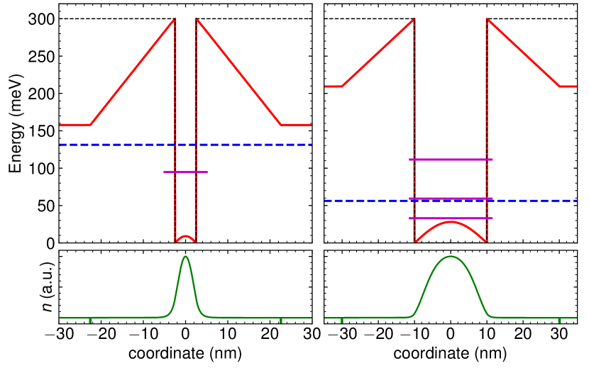
The profiles of electrostatic potential and electron density is shown in Fig. 2 for the two QWs: for a relatively narrow 5 nm QW with the density cm-2 and for a relatively wide QW 20 nm with the density cm-2.
IV Results
From the calculated wave functions in charged quantum well , we calculate the spin orbit constants , , and using Eqs. (4). The values of these constants as a function of electron density in the QW for few typical QW widths are presented in Fig. 3.
In symmetric GaAs/AlGaAs QWs with small electron population, the interface terms are comparable (about 30 percent) with bulk contribution when the QW width is relatively small, below 5 nm [14]. However, our current calculations show that for such thin QWs the change of the interface contribution with the change of the electron density is small. Quite the contrary, our calculations also demonstrate that the effect of 2D electron charge on the QW potential profile is much more pronounced in large QWs.
Indeed, from Fig. 3 it is clear that, at substantial 2D electron populations, for the wide QW with nm the value of the interface contribution parameters change significantly with changing the 2D electron density , unlike their almost independent on behavior in the narrow well with nm. Such change of , approximately two times with changing of from zero to maximum possible value, is of the same order of magnitude as the change of the bulk contribution to the Dresselhaus interaction, with changing of up to maximum possible value. Note that the main part of the bulk spin-orbit parameter is still much larger than interface contributions for the all studied QWs.
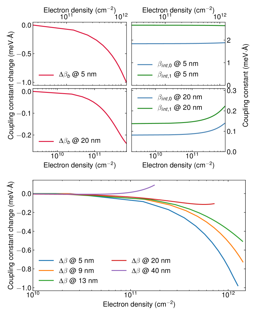
In lower panel of Fig. 3 we present the numerical results for the change of the total Dresselhaus constant , which is defined as
| (10) |
as a function of electron density in QW. Note that the spin splitting constant can exhibit different types of dependencies on the electron density for different width of the quantum wells. For thin quantum wells, the interface contribution is relatively large, but it does not change with the electron density. In such QWs, the change of the spin splitting constant is defined by the change of bulk contribution to the spin splitting . When the QW is sufficiently large, the change of is defined by the interface constribution. However, in wide GaAlAs QWs the interface contribution is small compared with bulk contribution. Thus, the detailed calculations show that there are two distinct regimes of dependence of spin splitting constant on the electron concentration. For QW widths below 20nm it is mainly due to the bulk contribution, whereas for wider QWs it is due to the interface one.
The increase in the interface contribution to the Dresselhaus interaction has the following reason. Due to the Coulomb repulsion, 2D electrons in wide quantum wells are “pushed” from the well center to the regions near the interfaces and the relative significance of the interface spin-orbit terms substantially increases, depending on the 2D electron density. Due to the difference in the bulk Dresselhaus constants and in the materials of the barrier and of the well, the bulk contribution to the anisotropic spin-orbit interaction decreases with the increase of .
V Conclusion
We have shown that in GaAs/AlGaAs quantum wells with sufficiently high electron densities, at which the 2D electron charge significantly affects the profile of the heterostructure potential , the interface as well as the bulk contributions to the anisotropic Dresselhaus spin-orbit interaction noticably change as a function of electron density. This effect should be important in quantitative studies of spin-orbit effects in these systems.
Acknowledgments
Analysis of the heterostructure design, calculations of the electron wave functions and the spin-orbit constants, described in section II and in a part of section IV, was supported by the Russian Science Foundation (Grant 17-12-01265) and the Foundation for advancement of theoretical physics and mathematics “BASIS”.
References
- Winkler [2003] R. Winkler, Spin-orbit Coupling Effects in Two-Dimensional Electron and Hole Systems (Springer, Berlin, 2003).
- Žutić et al. [2004] I. Žutić, J. Fabian, and S. Das Sarma, Spintronics: Fundamentals and applications, Rev. Mod. Phys. 76, 323 (2004).
- Ivchenko [2005] E. L. Ivchenko, Optical Spectroscopy of Semiconductor Nanostructures (Alpha Science, 2005).
- Ganichev and Golub [2014] S. D. Ganichev and L. E. Golub, Interplay of Rashba/Dresselhaus spin splittings probed by photogalvanic spectroscopy — A review, physica status solidi (b) 251, 1801 (2014).
- Dresselhaus [1955] G. Dresselhaus, Spin-orbit coupling effects in zinc blende structures, Phys. Rev. 100, 580 (1955).
- Ogg [1966] N. R. Ogg, Conduction-band g-factor anisotropy in indium antimonide, Proceedings of the Physical Society 89, 431 (1966).
- Pfeffer and Zawadzki [1990] P. Pfeffer and W. Zawadzki, Conduction electrons in GaAs: Five-level kp theory and polaron effects, Phys. Rev. B 41, 1561 (1990).
- Pikus et al. [1988] G. E. Pikus, V. A. Maruschak, and A. N. Titkov, Fiz. Tekh. Poluprovdn. 22, 185 (1988), [Sov. Phys. Semicond. 22, 115 (1988)].
- Cardona et al. [1988] M. Cardona, N. E. Christensen, and G. Fasol, Relativistic band structure and spin-orbit splitting of zinc-blende-type semiconductors, Phys. Rev. B 38, 1806 (1988).
- Luo et al. [2009] J.-W. Luo, G. Bester, and A. Zunger, Full-zone spin splitting for electrons and holes in bulk GaAs and GaSb, Phys. Rev. Lett. 102, 056405 (2009).
- Nestoklon et al. [2012] M. O. Nestoklon, S. A. Tarasenko, J.-M. Jancu, and P. Voisin, Spin splitting of electron states in (110) quantum wells: Symmetry analysis and kp theory versus microscopic calculations, Phys. Rev. B 85, 205307 (2012).
- Tarasenko et al. [2015] S. A. Tarasenko, M. V. Durnev, M. O. Nestoklon, E. L. Ivchenko, J.-W. Luo, and A. Zunger, Split dirac cones in HgTe/CdTe quantum wells due to symmetry-enforced level anticrossing at interfaces, Phys. Rev. B 91, 081302 (2015).
- Nestoklon et al. [2016] M. O. Nestoklon, S. A. Tarasenko, R. Benchamekh, and P. Voisin, Spin splitting of electron states in lattice-mismatched (110)-oriented quantum wells, Phys. Rev. B 94, 115310 (2016).
- Alekseev and Nestoklon [2017] P. S. Alekseev and M. O. Nestoklon, Effective one-band approach for the spin splittings in quantum wells, Phys. Rev. B 95, 125303 (2017).
- Alekseev [2013a] P. S. Alekseev, Fiz. Tekh. Polupr. 47, 1253 (2013a), [Semiconductors 47, 1241 (2013)].
- Alekseev [2013b] P. S. Alekseev, Pis’ma v Zh. Exp. Teor. Fiz. 98, 92 (2013b), [JETP Lett. 98, 84 (2013)].
- Devizorova and Volkov [2013] Z. A. Devizorova and V. A. Volkov, Pis’ma v Zh. Exp. i Teor. Fiz. 98, 110 (2013), [JETP Lett. 98, 101 (2013)].
- Chang and Schulman [1983] Y. Chang and J. N. Schulman, Modification of optical properties of GaAs-Ga1-xAlxAs superlattices due to band mixing, Applied Physics Letters 43, 536 (1983).
- Schulman and Chang [1985] J. N. Schulman and Y.-C. Chang, Band mixing in semiconductor superlattices, Phys. Rev. B 31, 2056 (1985).
- Chang and Schulman [1985] Y.-C. Chang and J. N. Schulman, Interband optical transitions in GaAs-Ga1-xAlxAs and InAs-GaSb superlattices, Phys. Rev. B 31, 2069 (1985).
- Aleiner and Ivchenko [1992] I. L. Aleiner and E. L. Ivchenko, Pis’ma Zh. Eksp. Teor. Fiz. 55, 662 (1992), [JETP Lett. 55, 692 (1992)].
- Ivchenko et al. [1993] E. L. Ivchenko, A. Y. Kaminskii, and I. L. Aleiner, ZhETF 104, 3401 (1993), [JETP 77, 609 (1993)].
- Vervoort et al. [1999] L. Vervoort, R. Ferreira, and P. Voisin, Spin splitting of the subbands of InGaAs-InP and other “no common atom” quantum wells, Semicond. Science and Technology 14, 227 (1999).
- Rössler and Kainz [2002] U. Rössler and J. Kainz, Microscopic interface asymmetry and spin-splitting of electron subbands in semiconductor quantum structures, Solid State Communications 121, 313 (2002).
- Alekseev and Nestoklon [2020] P. S. Alekseev and M. O. Nestoklon, Erratum: Effective one-band approach for the spin splittings in quantum wells [Phys. Rev. B 95, 125303 (2017)], Phys. Rev. B 102, 239902 (2020).
- Umansky et al. [2009] V. Umansky, M. Heiblum, Y. Levinson, J. Smet, J. Nübler, and M. Dolev, MBE growth of ultra-low disorder 2DEG with mobility exceeding 35106cm2/Vs, Journal of Crystal Growth 311, 1658 (2009), international Conference on Molecular Beam Epitaxy (MBE-XV).
- Umansky et al. [1997] V. Umansky, R. de Picciotto, and M. Heiblum, Extremely high-mobility two dimensional electron gas: Evaluation of scattering mechanisms, Applied Physics Letters 71, 683 (1997).
- Fu and Egues [2015] J. Fu and J. C. Egues, Spin-orbit interaction in GaAs wells: From one to two subbands, Phys. Rev. B 91, 075408 (2015).
- Calsaverini et al. [2008] R. S. Calsaverini, E. Bernardes, J. C. Egues, and D. Loss, Intersubband-induced spin-orbit interaction in quantum wells, Phys. Rev. B 78, 155313 (2008).
- Golub and Ivchenko [2004] L. E. Golub and E. L. Ivchenko, Spin splitting in symmetrical sige quantum wells, Phys. Rev. B 69, 115333 (2004).
- Nestoklon et al. [2006] M. O. Nestoklon, L. E. Golub, and E. L. Ivchenko, Spin and valley-orbit splittings in SiGe/Si heterostructures, Phys. Rev. B 73, 235334 (2006).
- Nestoklon et al. [2008] M. O. Nestoklon, E. L. Ivchenko, J.-M. Jancu, and P. Voisin, Electric field effect on electron spin splitting in quantum wells, Phys. Rev. B 77, 155328 (2008).
- Dettwiler et al. [2017] F. Dettwiler, J. Fu, S. Mack, P. J. Weigele, J. C. Egues, D. D. Awschalom, and D. M. Zumbühl, Stretchable persistent spin helices in GaAs quantum wells, Phys. Rev. X 7, 031010 (2017).