Thin-suspended 2D Materials: Facile, Versatile, and Deterministic Transfer Assembly
Abstract
We report a deterministic 2D material (2DM) transfer method to assemble any-stacking-order heterostructures incorporating suspended ultra-thin 2D materials, such as single-layer graphene (SLG) and bilayer graphene (BLG). The transfer procedure relies on a single-step preparation nitrocellulose micro-stamp, which combines both outstanding adhesion and softness. It permits the dry pick-up of naked 2D crystals (graphene, MoS2, and hBN) directly from a SiO2 substrate, and to precisely transfer them on substrates or trenches. Optical and Raman data show that no significant defect is introduced upon transfer, even in suspended SLG and BLG. The areas transferred range up 1000 m2 on substrate. High-yield transfer of suspended ultra-thin 2DM does not require critical point drying for areas up to 15 m2 or suspension heights down to 160 nm. To demonstrate the method’s capabilities, we assembled on-substrate and suspended optical cavities tuning BLG’s Raman scattering intensity by factors of 19 and 4, respectively. This resilient and rapid 2DM transfer procedure will accelerate the fabrication of many heterostructures and permit versatile suspension of 2DMs for research in twistronics, straintronics, and nano-opto-electro-mechanical systems (NOEMS).
Advances in the ability to mechanically transfer, align, and stack 2D materials (2DMs)1, 2, to form pristine heterostructures3, 4, have greatly accelerated experiments in quantum electron transport 5, 6, 7, 8 and optoelectronics 9, 10 over the last several years. The wide array of 2DM transfer methods now available 2, 1 can assemble most of the possible vertically-stacked heterostructures, with major exceptions for suspended 2DMs. Moreover, the state-of-the-art 2D transfer methods 11, 1, 2 are complex and time consuming since they often requires using a stamp made with two separate films, such as polypropylene carbonate (PPC) and polydimethylsiloxane (PDMS). There is a need to develop a single-material stamp combining the adhesion of PPC and softness of PDMS for more resilient, versatile, and faster transfers.
Presently, there is no flexible (any 2DM, any stacking order) and deterministic (with alignment) procedure to assemble heterostructures incorporating 2DMs and layers of vacuum/air and suspended ultra-thin 2DMs. Indeed, previous transfer methods for heterostructures incorporating suspended 2DMs have either used thick-suspended crystals12, 13, 14, non-deterministic transfer of thin-suspended 2DMs15, or developed single-purpose custom micro/nanofabrication routes for each device geometry16, 17, 18, 19. There are many motivations for integrating suspended 2DMs in precisely assembled heterostructures. Such devices would permit unprecedented levels of simultaneous control of electronics, mechanics, optics, and their interactions in nano-opto-electro-mechanical systems (NOEMS)13, 20, 21. For example, vacuum layers offer a uniquely different index of refraction to optimize exciton binding energy and lifetime in 2DMs 22. In quantum transport studies of twisted bilayers (twistronics)23, 24, 25, properly designed suspension would decouple the mechanically sensitive bilayers from the substrate to permit strain-engineering26, 27, 28 of their quantum phases 29, 30, 6. Additionally, stacking 2D suspended nano-electro-mechanical systems (NEMS) on top of 2D mirrors can create optical cavities31, 32, 33 enhancing light-matter interactions and hybridizing photonics with NEMS physics 20, 34, 35, 17.
Here we present the development of a 2DM transfer method able to dry pick-up ultra-thin naked (i.e. not encapsulated) crystals directly from SiO2, and then transfer them on substrates or trenches using only microliters of mild solvents. Our facile stamping procedure relies on a nitrocellulose micro-stamp ( 200 m wide) deposited on a glass slide actuated by a micromanipulator. This microstamp is much simpler to prepare than previously used PPC/PDMS stamps 11. The micro-stamp improves both the optical contrast and manipulation of thin 2DMs. It takes less than one hour to complete the transfer of a crystal (graphene, MoS2, and hBN) with areas up to 1000 m2. A single robust protocol was developed to transfer and align crystals onto different substrates (SiO2, hBN, aluminum). We verify via optical imaging and Raman spectroscopy, that the crystals are not damaged during transfer and can be aligned with a 1 m accuracy. We demonstrate the assembly of high-quality heterostructures both on substrate (e.g. BLG/hBN/Al) and suspended over hBN trenches (e.g. BLG/air/SiO2/Si). No critical point drying is required to transfer ultra-thin 2D areas up to 15 m2 or suspension heights down to 160 nm. A first application of this transfer assembly is demonstrated by fabricating optical cavities able to engineer the Raman scattering intensity (Raman factor) of BLG. We find a quantitative agreement between first principle calculations and experimental data of the BLG Raman factor, , and for its underlying exclusive light absorption , on several BLG/hBN/Al and BLG/Air/SiO2/Si cavities. The is tuned by factors of 19 and 3.8 in supported and suspended BLG heterostructures, respectively. Given the unique electronic and optical properties of BLG, maximizing and would bring new opportunities in light harvesting and photo-electric devices 31, 32, 10.
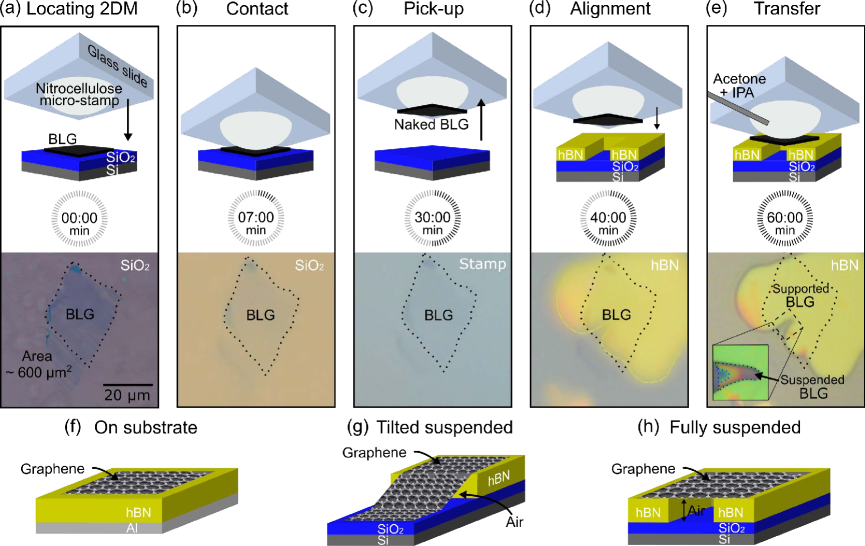
Deterministic stamping of any-stacking-order and suspended ultra-thin 2DMs such as SLG and BLG has been out of reach so far. A first challenge explaining this is that while SiO2 substrates permit an easy identification of thin exfoliated crystals 36, dry pick-up of naked 2DMs on SiO2 has not generally been possible due to the strong substrate adhesion 2. Secondly, the controlled pick-up and transfer of one crystal, leaving nearby flakes untouched, is not trivial and best done with a three-dimensional micro-stamp 14. Lastly, the stamping process of thin-suspended crystals requires finesse to avoid tearing of the crystal, or collapse of the suspended layer due to capillary forces 37. Figure 1 summarizes the main steps of our deterministic any-stacking-order and thin-suspended 2DM transfer. It rests on a dry nitrocellulose micro-stamp which strongly adheres to 2DMs for pick-up. This stamp acts as a micro-lens improving the imaging contrast of ultra-thin crystals, and as a micro-manipulator able to gently handle them. The micro-stamp can be dissolved with mild solvents. Our stamping instrumentation is similar to the one used in previous transfer methods 12, 1 (see the Supporting Information S1). It consists of a rotating () stage holding the substrate, micro manipulators translating the glass slide and micro-stamp, and a long working distance optical microscope for live monitoring the transfer. A complete transfer procedure as shown in Figure 1 can be done under 60 minutes. The procedure is the same for various materials: SLG, BLG, FLG, hBN, and MoS2, and does not require any temperature control 38, microfabrication step, or harsh chemical.
The transfer procedure starts with Figure 1a, where we position a micro-stamp above the 2DM to be picked-up. The preliminary preparation of the micro-stamp, substrates, and 2D crystals is discussed in detail in the Supporting Information S1. A fresh micro-stamp is prepared before each transfer. The stamp is roughly a half-dome with dimensions of 500 m, while its contact area during transfer is limited to 200 m 200m. To create a micro-stamp, we deposit a sub-microliter amount of a commercially available nitrocellulose polymer solution (Extra LifeTM No Chip Top Coat - Revlon) on a glass slide, and let it dry for approximately 7 minutes. The stamp permits high resolution optical imaging of 2DMs when looking through it, as shown for a typical BLG crystal at the bottom of Figure 1a. Images of the same crystal are shown at each stage of the transfer in Figure 1b-e. In Figure 1b, the micro-stamp is first carefully aligned with the target crystal, and then brought down at a speed of 50 m/s until it makes contact (detected by a sudden change of color). The stamp is pressed down gently so that it only makes contact with the crystal and its immediate surrounding area. A one-way pressing down motion is required (i.e. no back and forth) to avoid deforming the micro-stamp and inducing folding of the crystal 14. The contact is maintained for 20 minutes to promote strong adhesion.
The stamp is then raised to pick-up the 2DM from the substrate, as shown in Figure 1c. Such a dry pick-up directly from SiO2 is not possible with most previously reported stamps such as polydimethylsiloxane (PDMS) 12, 39, polymethylmethacrylate (PMMA) 40, thermal release tape (TRP) 41, polyvinyl alcohol (PVA) 1, and polypropylene carbonate (PPC) 23, 42. A key parameter to ensure a defect-free pick-up is to control the raising speed. We found that 250 m/s is ideal for multilayer 2DMs, and 500 m/s is best for ultra-thin materials. In Figure 1d, the target substrate is first placed underneath the micro-stamp/2DM assembly with micron precision, and then the stamp is lowered. An example of the alignment precision is seen by comparing the contour of the BLG crystal in Figures 1d and 1e, and found to be 2 m in this instance. The stamp is lowered ( 5 m/s) until it contacts the new substrate. We monitor the pressure applied during the transfer by ensuring that the stamp does not contact the SiO2 immediately surrounding the hBN substrate.
Figure 1e shows how the stamp is pressed against the target substrate. The following step is to dissolve the stamp using sub-milliliter volumes of acetone, followed by isopropyl alcohol (IPA), to cleanly transfer the 2DM (Supporting Information S1). A pipette is first used to insert acetone into the spacing between the glass slide anchoring the micro-stamp and the substrate. The acetone rapidly dissolves the nitrocellulose and releases the 2DM. Once the stamp is dissolved, and before the acetone evaporates, we raise the glass slide by 500 m and use the same pipette to flush with IPA. We repeat this IPA flushing to clean any residue. At this point the 2DM has been transferred to the new substrate, but is covered with IPA (a low surface tension solvent). For suspended crystal transfers, we control the drying (evaporation rate) of IPA to avoid large capillary forces. By raising or lowering the glass slide we can modulate the evaporation rate (see Supporting Information S1). This permits a delicate transfer of suspended crystals, such as the suspended BLG region in Figure 1e. The complete transfer sequence is shown in the Supporting Movie 1. Figures 1f-h show the three main heterostructure geometries we discuss in the rest of this work: (f) on-substrate BLG/hBN/Al, (g) tilted-suspended BLG/air(variable thickness)/SiO2/Si, and (h) fully-suspended BLG/air/SiO2/Si.
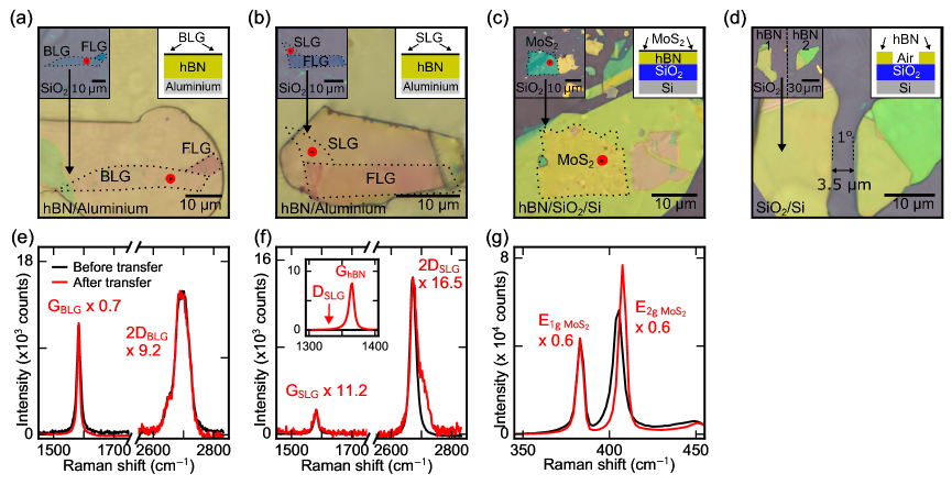
In Figure 2, we present large area heterostructures incorporating SLG, BLG, FLG, hBN, and MoS2(10-nm-thick) crystals, without encapsulation, which were assembled as per Figure 1. To create the heterostructures in the main panels of Figures 2a,b we first evaporated a 40 nm-thick film of Aluminum on SiO2/Si substrates, while for the ones in Figure 2c,d we used bare SiO2/Si substrates. The Al or Si bottom layers of the heterostructures will later on act as back-plane optical mirrors. The next step of fabrication was to deterministically transfer thick ( 400 nm) and large area hBN crystals (up to 1000 m2) which will act as substrates for the ultra-thin crystals, and will later define the thickness of the planar optical cavities. Then, we picked-up the thin 2D crystals shown in the insets of Figures 2a-c. They were transferred without any tearing or folding, and very few bubbles, as visible in the main panels. The top-right insets show the cross-section of the final stacks. The transferred crystals were a few hundred m2 and included SLG, BLG, few-layer graphene (FLG), and MoS2.
Figure 2d displays how we can controllably position two 2DMs at deterministic relative positions. Two separate transfers were used to pick-up the two hBN crystals on SiO2 shown in the top-left inset of Figure 2d, and to assemble them into a narrow hBN trench. The quality of both the rotational alignment (one-degree precision) and translational (one-micron precision) are clearly visible in the main panel of Figure 2d. Such trenches can be used for a lithography-free assembly of suspended heterostructures, by stamping a 2DM on top of the trench.
The Raman data shown in Figures 2e-g were taken at the red-marker locations in Figures 2a,b,c. We acquired Raman spectra at many spatial locations (Supporting Information S2), but since there is no significant spatial variation we show a single spectrum for clarity. The black data were acquired before transfer of the crystals, and the red data after the transfers. As expected, the relative heights of the G and 2D graphene Raman peaks are different before and after transfer due to optical interferences inside of the heterostructures (discussed below). The red data in Figures 2e-g are scaled as indicated. The widths of the Raman resonances are the same before and after transfer, and there is no resolvable D-peak in the graphene spectra (inset of Figure 2f). This indicates that no microscopic disorder was introduced in the crystals during stamping. Out of the 21 on-substrate heterostructure assemblies we carried out, 18 were completely successful and similar to the ones in Figure 2 (see Supporting Information S2), two were partially successful (some tearing) but produced the desired planar heterostructures, and only one was not transferred.
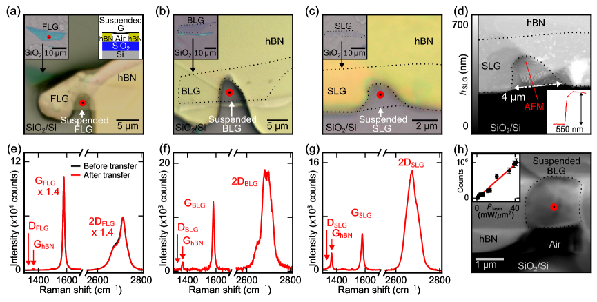
Figure 3 shows four different thin-suspended-graphene/air/SiO2/Si heterostructures assembled following the procedure in Figure 1. Optical images (Figures 3a-c), AFM data (Figure 3d), Raman data (Figures 3e-g), and titled-SEM imaging (Figure 3h), and detailed Supplementary Information for two additional suspended devices (Figures S8-S9), show that the thin-suspended crystals can be transferred without tearing, folding, or the introduction of microscopic defects. The transferred crystals were precisely aligned over hBN trenches, and suspended in close proximity to a back plane of SiO2. The suspension height, which is crucial to maximize optical resonances or electrostatic gating, is as small as 550 nm in Figure 3, down to 340 nm in another suspended device (Supporting Information S3), and as small as 160 nm in a tilted-suspended device presented below. The 2DM suspended areas in Figure 3 range up to 15 m2. The U-shaped hBN trenches we used form naturally during hBN exfoliation, and are ideal lithography-free trenches for graphene suspension. Figure 3a-c, show suspended graphene crystals after transfer (before transfer in top-left insets). The final heterostructures’ geometry is shown in the top-right inset of Figure 3a. The suspended FLG area’s optical contrast is clearly visible in Figure 3a, and black dotted lines show the contours of the BLG and SLG crystals in Figures 3b,c. Additional evidence of the complete suspension of the SLG crystal from Figure 3c, is shown in the AFM image of Figure 3d. The bottom left inset, is an AFM trace extracted at the location of the red line in the main panel, and confirms the SLG suspension at a height of 550 nm above the substrate.
Figures 3e-g show Raman data acquired at the red-marker locations on the graphene crystals before (black data) or after (red data) suspension. Additional Raman data before and after suspension are shown in Figure S8. While the relative height of the Raman resonances changes before/after due to optical interferences inside the heterostructure, the width of the resonances remains the same and no graphene D-peak is visible after suspension. Figure 3h shows a tilted-SEM image of a suspended BLG after transfer. It demonstrates that the suspended surface is wrinkle-free and of uniform height. The top left inset shows the integrated area under the Raman G-peak (number of scattering events) as a function of laser power measured at the red marker location. The linear relationship confirms that the suspended crystal does not heat up over a laser power range which exceeds the ones we used for our Raman data acquisitions, i.e. 0 - 40 mW/m2 for 10 seconds. We carried out 16 suspended crystal transfers and 15 were successful, and similar to the ones shown in Figure 3 (see Supporting Information S3). This high-yield and precise transfer of ultra-thin suspended 2DMs could facilitate the fabrication of novel NEMS and NOEMS. We demonstrate a first example in Figure 4.
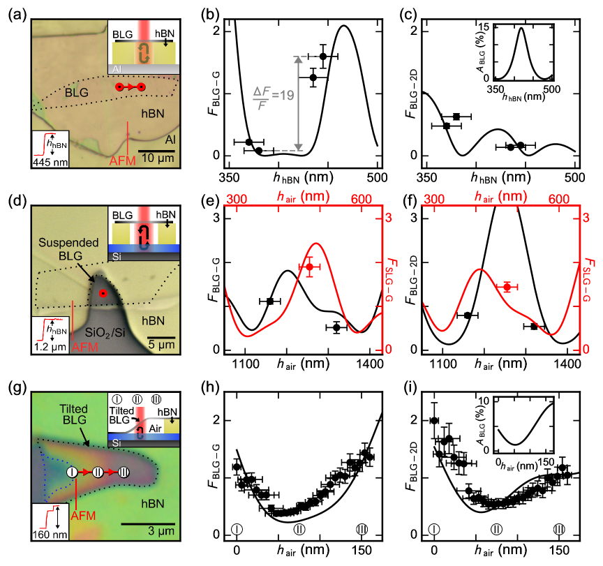
Developing heterostructures for optoelectronics applications9, and exploring 2D light-matter interactions20, often requires increasing the very small bare light absorption in ultra-thin 2DMs 17. Planar heterostructures can act as optical interferometric cavities to greatly enhance light absorption and Raman scattering in 2DMs, including graphene 43, 32 and 2D transition metal dichalcogenides (TMDs) 33. While previous work has focused on maximizing absorption in the infrared range 32, 44 and for on-substrate 2DMs, here we focus on absorption of visible light in suspended BLG. In Figure 4, we study our BLG/hBN/Al and BLG/air/SiO2/Si heterostructures as optical cavities, where the BLG acts as a low-reflectivity input mirror and the substrate (Al or Si) acts as a high-reflectivity bottom mirror. We study these optical cavities using Raman spectroscopy, which provides clearly distinctive signatures of light scattering and absorption in the graphene layer than scattering in other parts of the heterostructures. The BLG Raman factor, , is defined as the ratio of the integrated BLG Raman count in an heterostructure and the same Raman count in BLG when the crystal is entirely surrounded by vacuum, i.e. there are no optical interferences (see Supporting Information S4)43. The quality of our structures permits a quantitative tuning of light interferences. We demonstrate experimentally a widely tunable , and calculate the associated exclusive light absorption . This could open up opportunities to generate strong light-matter interactions in 2D NEMS31, for instance in suspended BLG twistronics8 NOEMS.
Figure 4a is a top view of one of four BLG/hBN/Al(40 nm) heterostructures, and its 445 15 nm. The red line in Figure 4a shows the location of the AFM trace displayed at the bottom left of the panel. The solid markers in Figure 4b-c show the measured G-peak and 2D-peak Raman factors, and , versus . The solid traces are zero-fit-parameter theoretical calculations. They are based on Fresnel’s equations and the known indices of refractions of the media in the heterostructures (see Supporting Information S4). To report experimental , we first calibrated the raw experimental Raman counts with respect to the theory. This calibration was done by carefully (Supporting information S4), and reproducibly, measuring the BLG Raman counts on BLG/SiO2(310-nm)/Si devices, for which the theoretical Raman factors are understood 43. We found that in our experimental setup, a 1.0 Raman factor corresponds to 38000 1000 and 125000 4000 counts of G and 2D Raman events, at a laser power density of 1.0 mW/m2 for 10 seconds. This single reference point was used to calibrate all values reported.
There is a good agreement between the data and model in Figures 4b-c, and can be tuned by 19 folds. This could have an application, for instance, to strongly enhance weak Raman signals predicted in many-body phase transitions 45 without requiring a disruptive increase in laser power. We calculated as a function of , using the same Fresnel coefficients as , and show the result in the inset of Figure 4c. This strongly supports that the exclusive light absorption of BLG, at the 532-nm laser wavelength, can be modulated from less than 1 to over 10 in our heterostructures. Figure 4d is a uniformly suspended BLG over a hBN trench, which is itself placed on a SiO2/Si substrate. The red line shows the location of the AFM trace shown in the bottom inset which gives . Figure 4e-f display the measured (solid markers) and calculated (solid traces) and versus suspension height, , for the device in Figure 4d and two more (one BLG, one SLG). The left and bottom axes are for the BLG data, and the right and top axes for the SLG data.
Figure 4g shows a top view of tilted-suspended BLG/air(variable thickness)/SiO2/Si heterostructure, and the top-right inset is a diagram of its cross-section. The labeled regions I, II, and III correspond to the areas of the BLG where the air-spacer thickness is respectively 0 nm, variable from 0 to 160 nm, and a constant 160 nm. A tilted structure is an ideal platform to demonstrate the tuning of light interferences as a function of in a single device. Figure 4h,i show and data (solid markers) and model (solid traces) versus measured on this tilted device. We observe a quantitative agreement between the data and model for both Raman modes. The G Raman factor was continuously tunable by a factor up to 3.8 in Figure 4h. The horizontal error bars in Figure 4h,i arise mostly from the uncertainty on the exact suspension profile of the device in Figure 4g (see Supporting Information S4). The inset of Figure 4i presents the calculated , which is widely tunable. We remark that reaches much closer to zero in the inset of Figure 4c, where the back-plane mirror used is aluminum instead of Si. While we have focused this study on lithography-free fabrication, introducing an Al mirror underneath a suspended BLG can be done, and will permit in situ electrostatic gate-tuning of , leading to vastly tunable and photo-electronic interactions in NOEMS46. Taken collectively, the agreement between Raman measurements and theoretical calculations in Figure 4 supports that we can transfer both suspended and on-substrate ultra-thin crystals of sufficient quality to manipulate their Raman factor, and exclusive light absorption.
In conclusion, we presented a 2DM transfer and assembly method based on a nitrocellulose micro-stamp able to stamp crystals in any-stacking order and incorporate suspended 2DMs. This method is a much needed simplification and extension of the current state-of-the-art PPC/PDMS stamping procedure 11, 1, 2, and will contribute to accelerate research in 2DMs. It permits the dry pick-up of 2D crystals directly from SiO2 substrates and to transfer them with precise alignment. A complete transfer takes under 60 minutes and has a success rate around 95. Most distinctively, this method can be used to transfer suspended ultra-thin materials such as monolayer and bilayer graphene over areas 10 m2, and suspension heights as low as 160 nm without critical point drying. Careful Raman spectroscopy and optical imaging showed no microscopic disorder, tear or a significant density of bubbles in the transferred materials. We demonstrated the assembly of planar optical cavities able to broadly tune BLG’s Raman scattering intensity, by up to 19 folds in on-substrate devices and nearly 4 folds in suspended structures. We calculated that the BLG exclusive light absorption can be engineered by a similar ratio. Our fabrication method fills a major gap in previous transfer methods by making possible a versatile transfer of suspended 2DMs (any material, stacking-order, substrate) all the way down to the ultra-thin limit (SLG, BLG). We foresee that this fabrication route can create heterostructures suited for exploring the interplays of nanoscale mechanics, optics, and electronics, for instance in twistronics 29, 24, 25, straintronics26, 27, 28, and optoelectronics 22, 20, 34, 35, 17.
This work was supported by NSERC (Canada), CFI (Canada), and Concordia University. We acknowledge usage of the QNI (Quebec Nano Infrastructure) cleanroom network.
1 Contributions
IGR and FCRM made equal contributions. They led the development of the methods, fabrication of the samples, measurements, data analysis, and calculations. ARC conceived and supervised the project, he made contributions to all aspects of the project. WW contributed to sample fabrication. GJM contributed to Raman measurements and data analysis. IGR, FCRM, and ARC wrote the manuscript, and all authors reviewed the manuscript.
2 Associated Content
Supporting Information: Detailed step-by-step description of the 2DM transfer method, information about all on-substrate heterostructures transferred, information about all suspended heterostructures transferred, description of the theoretical calculations of the Raman factors (and light absorption) and their comparison to the experimental data. (PDF)
Supporting Movie: Video of the step-by-step 2DM transfer procedure.
References
- Frisenda et al. 2018 Frisenda, R.; Navarro-Moratalla, E.; Gant, P.; Pérez De Lara, D.; Jarillo-Herrero, P.; Gorbachev, R. V.; Castellanos-Gomez, A. Recent progress in the assembly of nanodevices and van der Waals heterostructures by deterministic placement of 2D materials. Chemical Society Reviews 2018, 47, 53–68
- Fan et al. 2020 Fan, S.; Vu, Q. A.; Tran, M. D.; Adhikari, S.; Lee, Y. H. Transfer assembly for two-dimensional van der Waals heterostructures. 2D Mater. 2020, 7, 022005
- Novoselov et al. 2016 Novoselov, K. S.; Mishchenko, A.; Carvalho, A.; Castro Neto, A. H. 2D materials and van der Waals heterostructures. Science 2016, 353, aac9439
- Liu et al. 2019 Liu, Y.; Huang, Y.; Duan, X. Van der Waals integration before and beyond two-dimensional materials. Nature 2019, 567, 323–333
- Shen et al. 2020 Shen, C. et al. Correlated states in twisted double bilayer graphene. Nature Phys. 2020, 16, 520
- Li et al. 2019 Li, J. I. A.; Shi, Q.; Zeng, Y.; Watanabe, K.; Taniguchi, T.; Hone, J.; Dean, C. R. Pairing states of composite fermions in double-layer graphene. Nature Physics 2019, 15, 898–903
- Yankowitz et al. 2019 Yankowitz, M.; Ma, Q.; Jarillo-Herrero, P.; LeRoy, B. J. van der Waals heterostructures combining graphene and hexagonal boron nitride. Nature Reviews Physics 2019, 1, 112–125
- Song and Gabor 2018 Song, J. C. W.; Gabor, N. M. Electron quantum metamaterials in van der Waals heterostructures. Nat. Nanotechnology 2018, 13, 986–993
- Rivera et al. 2018 Rivera, P.; Yu, H.; Seyler, K. L.; Wilson, N. P.; Yao, W.; Xu, X. Interlayer valley excitons in heterobilayers of transition metal dichalcogenides. Nat. Nanotechnol. 2018, 13, 1004–1015
- Deilmann et al. 2020 Deilmann, T.; Rohlfing, M.; Wurstbauer, U. Light–matter interaction in van der Waals hetero-structures. J. Phys.: Condens. Matter 2020, 32, 333002
- Wang et al. 2013 Wang, L.; Meric, I.; Huang, P. Y.; Gao, Q.; Gao, Y.; Tran, H.; Taniguchi, T.; Watanabe, K.; Campos, L. M.; Muller, D. A.; Guo, J.; Kim, P.; Hone, J.; Shepard, K. L.; Dean, C. R. One-Dimensional Electrical Contact to a Two-Dimensional Material. Science 2013, 342, 614–617
- Castellanos-Gomez et al. 2014 Castellanos-Gomez, A.; Buscema, M.; Molenaar, R.; Singh, V.; Janssen, L.; Van Der Zant, H. S. J.; Steele, G. A. Deterministic transfer of two-dimensional materials by all-dry viscoelastic stamping. 2D Materials 2014, 1, 011002
- Singh et al. 2014 Singh, V.; Bosman, S. J.; Schneider, B. H.; Blanter, Y. M.; Castellanos-Gomez, A.; Steele, G. A. Optomechanical coupling between a multilayer graphene mechanical resonator and a superconducting microwave cavity. Nature Nanotechnol. 2014, 9, 820–824
- Wakafuji et al. 2020 Wakafuji, Y.; Moriya, R.; Masubuchi, S.; Watanabe, K.; Taniguchi, T.; Machida, T. 3D Manipulation of 2D Materials Using Microdome Polymer. Nano Lett. 2020, 20, 2486–2492
- Li et al. 2015 Li, B. et al. Scalable Transfer of Suspended Two-Dimensional Single Crystals. Nano Lett. 2015, 15, 5089–5097
- Liu et al. 2019 Liu, Y.; Abhilash, T. S.; Laitinen, A.; Tan, Z.; Liu, G. J.; Hakonen, P. Dry transfer method for suspended graphene on lift-off-resist: simple ballistic devices with Fabry–Pérot interference. Nanotechnology 2019, 30, 25LT01
- Zhang et al. 2019 Zhang, X.; De-Eknamkul, C.; Gu, J.; Boehmke, A. L.; Menon, V. M.; Khurgin, J.; Cubukcu, E. Guiding of visible photons at the ångström thickness limit. Nat. Nanotechnol. 2019, 14, 844–850
- Yigen and Champagne 2014 Yigen, S.; Champagne, A. R. Wiedemann-Franz Relation and Thermal-Transistor Effect in Suspended Graphene. Nano Letters 2014, 14, 289–293
- Bolotin et al. 2008 Bolotin, K. I.; Sikes, K. J.; Jiang, Z.; Klima, M.; Fudenberg, G.; Hone, J.; Kim, P.; Stormer, H. L. Ultrahigh electron mobility in suspended graphene. Solid State Commun. 2008, 146, 351–355
- Midolo et al. 2018 Midolo, L.; Schliesser, A.; Fiore, A. Nano-opto-electro-mechanical systems. Nat. Nanotechnol. 2018, 13, 11–18
- Roy et al. 2018 Roy, S. K.; Sauer, V. T. K.; Westwood-Bachman, J. N.; Venkatasubramanian, A.; Hiebert, W. K. Improving mechanical sensor performance through larger damping. Science 2018, 360, eaar5220
- Florian et al. 2018 Florian, M.; Hartmann, M.; Steinhoff, A.; Klein, J.; Holleitner, A. W.; Finley, J. J.; Wehling, T. O.; Kaniber, M.; Gies, C. The Dielectric Impact of Layer Distances on Exciton and Trion Binding Energies in van der Waals Heterostructures. Nano Lett. 2018, 18, 2725–2732
- Kim et al. 2016 Kim, K. H.; Yankowitz, M.; Fallahazad, B.; Kang, S.; Movva, H. C. P.; Huang, S.; Larentis, S.; Corbet, C. M.; Taniguchi, T.; Watanabe, K.; Banerjee, S. K.; LeRoy, B. J.; Tutuc, E. van der Waals Heterostructures with High Accuracy Rotational Alignment. Nano Lett. 2016, 16, 1989–1995
- Hu et al. 2020 Hu, G.; Krasnok, A.; Mazor, Y.; Qiu, C.-W.; Alù, A. Moiré Hyperbolic Metasurfaces. Nano Letters 2020, 20, 3217–3224
- Weston et al. 2020 Weston, A. et al. Atomic reconstruction in twisted bilayers of transition metal dichalcogenides. Nature Nanotechnol. 2020, 15, 592–597
- Naumis et al. 2017 Naumis, G. G.; Barraza-Lopez, S.; Oliva-Leyva, M.; Terrones, H. Electronic and optical properties of strained graphene and other strained 2D materials: a review. Rep. Prog. Phys. 2017, 80, 096501
- McRae et al. 2019 McRae, A. C.; Wei, G.; Champagne, A. R. Graphene Quantum Strain Transistors. Physical Review Applied 2019, 11
- Zhang et al. 2020 Zhang, X.; Makles, K.; Colombier, L.; Metten, D.; Majjad, H.; Verlot, P.; Berciaud, S. Dynamically-enhanced strain in atomically-thin resonators. Nature Commun. 2020, 11, 5526
- Cao et al. 2018 Cao, Y.; Fatemi, V.; Fang, S.; Watanabe, K.; Taniguchi, T.; Kaxiras, E.; Jarillo-Herrero, P. Unconventional superconductivity in magic-angle graphene superlattices. Nature 2018, 556, 43–50
- Xian et al. 2019 Xian, L.; Kennes, D. M.; Tancogne-Dejean, N.; Altarelli, M.; Rubio, A. Multiflat Bands and Strong Correlations in Twisted Bilayer Boron Nitride: Doping-Induced Correlated Insulator and Superconductor. Nano Lett. 2019, 19, 4934–4940
- Song et al. 2015 Song, H.; Jiang, S.; Ji, D.; Zeng, X.; Zhang, N.; Liu, K.; Wang, C.; Xu, Y.; Gan, Q. Nanocavity absorption enhancement for two-dimensional material monolayer systems. Optics Express 2015, 23, 7120–7130
- Casalino et al. 2017 Casalino, M.; Sassi, U.; Goykhman, I.; Eiden, A.; Lidorikis, E.; Milana, S.; De Fazio, D.; Tomarchio, F.; Iodice, M.; Coppola, G.; Ferrari, A. C. Vertically Illuminated, Resonant Cavity Enhanced, Graphene–Silicon Schottky Photodetectors. ACS Nano 2017, 11, 10955–10963
- Epstein et al. 2020 Epstein, I.; Terrés, B.; Chaves, A. J.; Pusapati, V.-V.; Rhodes, D. A.; Frank, B.; Zimmermann, V.; Qin, Y.; Watanabe, K.; Taniguchi, T.; Giessen, H.; Tongay, S.; Hone, J. C.; Peres, N. M. R.; Koppens, F. H. L. Near-Unity Light Absorption in a Monolayer WS2 Van der Waals Heterostructure Cavity. Nano Letters 2020, 20, 3545–3552
- Eggleton et al. 2019 Eggleton, B. J.; Poulton, C. G.; Rakich, P. T.; Steel, M. J.; Bahl, G. Brillouin integrated photonics. Nature Photonics 2019, 13, 664–677
- Li et al. 2019 Li, H.-K.; Fong, K. Y.; Zhu, H.; Li, Q.; Wang, S.; Yang, S.; Wang, Y.; Zhang, X. Valley optomechanics in a monolayer semiconductor. Nature Photonics 2019, 13, 397–401
- Blake et al. 2007 Blake, P.; Hill, E. W.; Castro Neto, A. H.; Novoselov, K. S.; Jiang, D.; Yang, R.; Booth, T. J.; Geim, A. K. Making graphene visible. Appl. Phys. Lett. 2007, 91, 063124
- Ma et al. 2017 Ma, X.; Liu, Q.; Xu, D.; Zhu, Y.; Kim, S. J.; Cui, Y.; Zhong, L.; Liu, M. Capillary-Force-Assisted Clean-Stamp Transfer of Two-Dimensional Materials. Nano Lett. 2017, 17, 6961–6967
- Pizzocchero et al. 2016 Pizzocchero, F.; Gammelgaard, L.; Jessen, B. S.; Caridad, J. M.; Wang, L.; Hone, J.; Bøggild, P.; Booth, T. J. The hot pick-up technique for batch assembly of van der Waals heterostructures. Nat. Commun. 2016, 7, 11894
- Tao et al. 2018 Tao, L.; Li, H.; Gao, Y.; Chen, Z.; Wang, L.; Deng, Y.; Zhang, J.; Xu, J. B. Deterministic and Etching-Free Transfer of Large-Scale 2D Layered Materials for Constructing Interlayer Coupled van der Waals Heterostructures. Advanced Materials Technologies 2018, 3, 1700282
- Uwanno et al. 2015 Uwanno, T.; Hattori, Y.; Taniguchi, T.; Watanabe, K.; Nagashio, K. Fully dry PMMA transfer of graphene on h -BN using a heating/cooling system. 2D Mater. 2015, 2, 041002
- Kim et al. 2015 Kim, S. J.; Choi, T.; Lee, B.; Lee, S. Y.; Choi, K.; Park, J. B.; Yoo, J. M.; Choi, Y. S.; Ryu, J.; Kim, P.; Hone, J.; Hong, B. H. Ultraclean Patterned Transfer of Single-Layer Graphene by Recyclable Pressure Sensitive Adhesive Films. Nano Lett. 2015, 15, 3236–3240
- Kinoshita et al. 2019 Kinoshita, K.; Moriya, R.; Onodera, M.; Wakafuji, Y.; Masubuchi, S.; Watanabe, K.; Taniguchi, T.; Machida, T. Dry release transfer of graphene and few-layer h-BN by utilizing thermoplasticity of polypropylene carbonate. npj 2D Materials and Applications 2019, 3, 22
- Yoon et al. 2009 Yoon, D.; Moon, H.; Son, Y. W.; Choi, J. S.; Park, B. H.; Cha, Y. H.; Kim, Y. D.; Cheong, H. Interference effect on Raman spectrum of graphene onSiO2/Si. Phys. Rev. B 2009, 80, 125422
- Nematpour et al. 2019 Nematpour, A.; Lisi, N.; Piegari, A.; Lancellotti, L.; Hu, G.; Grilli, M. L. Experimental near infrared absorption enhancement of graphene layers in an optical resonant cavity. Nanotechnol. 2019, 30, 445201
- Maiti et al. 2017 Maiti, S.; Chubukov, A. V.; Hirschfeld, P. J. Conservation laws, vertex corrections, and screening in Raman spectroscopy. Phys. Rev. B 2017, 96, 014503
- Metten et al. 2016 Metten, D.; Froehlicher, G.; Berciaud, S. Monitoring electrostatically-induced deflection, strain and doping in suspended graphene using Raman spectroscopy. 2D Materials 2016, 4, 014004