††thanks: One of the authors, AAB, thanks CNPq for
the support during his stay at UFPE.
Large-Signal and High–Frequency Analysis of Nonuniformly Doped or Shaped PN-Junction Diodes
Anatoly A. Barybin
Electronics Department,
Saint-Petersburg State Electrotechnical University,
197376, Saint-Petersburg, Russia.
Edval J. P. Santos
edval@ee.ufpe.br / e.santos@expressmail.dk.
Laboratory for Devices and Nanostructures,
Engineering at Nanometer Scale Group,
Universidade Federal de Pernambuco, Recife-PE, Brasil.
Abstract
An analytical theory of nonuniformly doped or shaped PN-junction diodes submitted to
large-signals at high frequencies is presented. The resulting expressions
can be useful to evaluate the performance of semiconductor device
modeling software. The transverse averaging technique is employed
to reduce the three-dimensional charge carrier transport equations into
the quasi-one-dimensional form, with all physical quantities
averaged out over the longitudinally-varying cross section.
Although, it is assumed an axial symmetry, this approach gives rise
to useful analytic expressions for the static
current–voltage characteristics, the diffusion conductance, and diffusion
capacitance as a function of the signal amplitude and the cross
section non-uniformity.
Depending on the application, different levels of device
modeling are used to predict the behavior of electronic circuits. For
circuits with many devices, compact models are required to reduce the
simulation time. For circuit building blocks with a few devices, physical
models may be used to get further insight. Physics-based modeling requires
more computer resources, but it has the advantage of being valid at a wider
operating range, and offers easier to interpret parameters SSRF2004 .
When modeling a PN-junction, different operating conditions are possible,
such as: steady-state small-signal, steady-state large-sginal, DC, and
transient SSRF2004 ,YLY1994 ,RBD1995 ,RPFAC1993 .
The transverse averaging technique (TAT) allows the general
three-dimensional (3D) equations of semiconductor electronics to be converted
into the so-called quasi-one-dimensional (quasi-1D) form. The
quasi-1D equations involve all the physical scalar quantities (potential,
charge density, etc.) and longitudinal components of the vector quantities
(electric field, current density, etc.) in the form averaged over the
longitudinally-varying cross section and dependent only on the
longitudinal coordinate BS2007a . It was first applied to
derive analytical expressions for the depletion capacitance of the
PN-junctions with nonuniform doping impurity profile and cross-sectional
geometry peculiar to various real devices. It may also be useful
to P--N diode modeling GSBQSB2007 . This work does not apply to
avalanche type diodes, such as IMPATT, as no generation/ionization process
is included in the theory at this point SMS1981 .
Besides, the average one-dimensional equations also include the contour
integrals along interface lines which take into account the proper boundary
conditions between different domains of the semiconductor structure.
Such equations are completely equivalent to the initial three-dimensional
equations and in this respect are accurate except that they deal with
physical quantities averaged over the cross section of a nonuniform
semiconductor structure.
This paper is devoted to the generalization of the large-signal and
high-frequency theory of the charge carrier transport developed
previously for uniform PN-junctions BS2007a ,BS2007b ,SB2002
to nonuniform structures. Application
of the general TAT relations given in paper BS2007a to deriving
the quasi-1D drift-diffusion equations for nonuniform junctions is performed
in Sec. II. Spectral solution of the quasi-1D diffusion equations
for nonuniform PN-junctions is set forth in Sec. III.
Section IV deals with the derivation and analysis of the
external circuit current, which serves as a basis for obtaining the
static current–voltage characteristics (Sec. V) and the
dynamic impedance (Sec. VI) of the PN-junction diodes with
nonuniform cross section.
II Derivation of Quasi-One-Dimensional Drift-Diffusion Equations
for Nonuniform PN-Junctions
The initial equations for derivation of the quasi-1D drift-diffusion equations
of the nonuniform PN-junctions are the three-dimensional continuity
equations and the current density expressions SMS1981 :
for holes
(1)
for electrons
(2)
with the normal components of currents that obey the following
surface-recombination boundary
conditions SMS1981 :
(3)
and
(4)
Here and are the equilibrium and nonequilibrium densities
of minority carriers in the - and -regions,
and are the diffusion constant, mobility, and lifetime for
holes (electrons).
Integration of Eqs. (1) and (2) over the cross
section area by using the TAT relations BS2007a
produces the linear integrals along the contour bounding .
For holes, calculating the average and applying the 3-D extension of
Green’s Theorem in (Eq. 1), yields
(5)
(6)
Here are the nonequilibrium minority-carrier volume densities
taken at surface points of the structure, and is the surface
recombination velocity for holes (electrons).
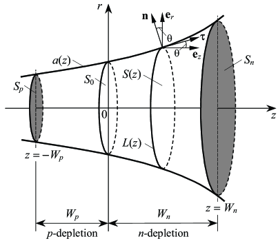
Figure 1: Axially symmetric PN-junction; the depletion layer is situated between the cross sections of area and of area .
Here the average quantities , and are
introduced BS2007a , while the
average mobility and diffusion constant for holes (and similar ones for
electrons) are defined as
For axially-symmetrical structures with , we have
so that the contour integrals in Eqs. (5) and (6)
with the boundary condition (3) assume the form
(7)
(8)
By substituting expressions (6)–(8) into
Eq. (5) and introducing the effective lifetime
to allow for both the volume and surface recombination
we arrive at the quasi-1D drift-diffusion equation for holes
injected into the -region:
(9)
Similarly, from the initial equations (2) and (4)
we obtain the quasi-1D drift-diffusion equation for electrons injected
into the -region:
(10)
All the average quantities , and
will be considered as phenomenologically given
parameters with dropping the bar sign over them for simplicity.
Quasi-one-dimensional equations (9) and (10)
are of the general form applicable for both the - and
PN-diodes. For low level of injection in the PN-diodes
we can assume for diode base so that
Eqs. (9) and (10) take the simplified form:
(11)
(12)
Not having a specific knowledge of surface properties, we shall assume
that and .
Then, from equations (11) and (12) follows the
quasi-one-dimensional diffusion equations for the excess
concentrations of holes, , and
electrons, , injected into
the appropriate neutral parts of the PN-diode BS2007a :
(13)
(14)
where is the diffusion
length for holes (electrons). The additional last term involving
takes into account the cross-sectional nonuniformity.
III Spectral Solution of Quasi-One-Dimensional Diffusion Equations
In general case, the voltage applied to the PN-junction consists of
the DC bias voltage and the AC harmonic signal :
(15)
Nonlinearity of electronic processes in the PN-junction produces the
frequency harmonics so that solutions of Eqs. (13)
and (14) have the form of Fourier series:
(16)
(17)
Real values of and are
provided with the following relations for the complex amplitudes:
and
.
Substitution of the required solutions (16) and
(17) into Eqs. (13) and (14) with
regard for the orthogonality of harmonics reduces to the following
equations for the harmonic amplitudes BS2007a :
(18)
(19)
where
As an analytical approximation to a mesa-like structure, the special
case of exponential change of the cross section
is considered, Eqs. (18) and
(19) turn into the linear equations BS2007a
(20)
(21)
Representing the desired solution in the form of ,
we obtain the following characteristic equation for Eqs. (20)
and (21):
(22)
The complex roots of Eq. (22) can be written as follows
(23)
where we have introduced the following notations:
for holes injected into the -region ()
(24)
for electrons injected into the -region ()
(25)
The general solutions of equations (20) and (21)
have the following form:
for holes injected into the -region ()
(26)
for electrons injected into the -region ()
(27)
In accordance with notations (24) and (25), always
Re and
Re
so that for the PN-diodes with thick bases we can
assume and , which eliminates the necessity
for boundary conditions on ohmic contacts. Taking into account formulas
(26) and (27) with ,
the general solutions (16) and (17) of
Eqs. (13) and (14) are written in the form
(28)
(29)
These expressions provide as
and as because of
Re and Re .
The constants and appearing in Eqs. (28)
and (29) can be found from the conventional injection boundary
conditions SMS1981 :
(30)
(31)
where for the applied voltage of the form (15) we have
introduced the function
(32)
Substitution of expressions (28) and (29)
into the boundary conditions (30) and (31) yields
(33)
By using the orthogonality property of harmonics in expansions
(33) it is easy to get the desired constants
(34)
where is the Fourier amplitude of the th harmonic for the
function given by formula (32), that is
(35)
Substitution of the function (32) into formula (35) gives
(36)
(37)
where we have used the modified Bessel functions of the first kind
of order () having the following integral
representation (see formula 8.431.5 in Ref. GR1980 ):
(38)
This function depends on , where is an
amplitude of the signal applied to the PN-junction and
.
Thus, with allowing for Eq. (34) the general solutions
(28) and (29) of the diffusion equations
(13) and (14) take the final form of spectral
expansions:
(39)
(40)
These expressions allow us to obtain the spectral composition of
the current flowing through the external circuit connected to the
PN-diode.
IV External Circuit Current for Semiconductor Diode with
Nonuniform Cross Section
The initial equation to derive an expression for the diode current is the
law of total current conservation:
(41)
following from Maxwell’s equation .
The transverse averaging technique applied to Eq. (41) gives
(42)
The similar equation outside the semiconductor, where currents are absent and
, has the following form:
(43)
where is an effective localization area of the fringe outside
field such that usually and
. The addition of Eqs. (42) and
(43) gives
(44)
If a semiconductor surface contains traps with the charge density
, there are the following boundary conditions on the contour
Barybin1986 :
(45)
In this case, two contour integrals in Eq. (44) cancel each
other and with allowing for inequality formula
(44) takes the form
(46)
The quantity in brackets of Eq. (46), being independent of ,
defines the external circuit current equal to
(47)
Here we have used expressions (6) and (8)
for the average hole current and the similar
expressions for the average electron current
(with dropping the bar sign over and ).
All the terms on the right of Eq. (47) depend on both
and but taken together at any cross section they yield
the external circuit current as a function of only time.
Restricting our consideration to the
PN-diodes with low injection, we can assume in
neutral parts of the - and -regions SMS1981 . Then the external
circuit current (47) is determined only by the averaged
diffusion currents taken at any cross section , for example,
at :
(48)
Neglecting recombination processes inside the PN-junction, which is
true if and SMS1981 , we can write
(49)
Substitution of relation (49) into Eq. (48) gives
the external circuit current (cf. Eq. (31) in Ref. BS2007a )
(50)
where and
are the excess concentrations of injected carriers determined by
formulas (39) and (40). Inserting these
formulas into expression (50), we finally obtain the
spectral representation for the external circuit current:
(51)
Here, the hole and electron contributions into the saturation current
of a thick PN-junction are defined, as it is generally
accepted SMS1981 , in the form
(52)
where
Expression (51) contains all the spectral components
of the external circuit current including the DC current for
and the AC current for which are of most interest for
our further consideration.
V Static Current–Voltage Characteristic of PN-Diode
with Nonuniform Cross Section
The term in series (51) numbered by corresponds to the DC
current , which by using (36) can be written in the form
of the static current–voltage characteristic:
(53)
Here we have introduced the saturation current for a nonuniform diode
(54)
and, in accordance with expressions (24) and (25)
for , have used the following notation:
(55)
For the uniform -junction (with ) we have
and so that
the static current-voltage characteristic
retains the form (53) with the usual saturation current
(56)
where as before superscript 0 marks the cross-sectional uniformity
(when and constant).
The modified Bessel function appearing in
Eq. (53) is completely the same as that obtained in our
paper BS2007a and it distinguishes our expression (53)
from the similar formula given in the known literature on semiconductor
electronics SMS1981 . Coincidence between them occurs only for
such small signals that and
. The function
reflects the effect of signal rectification, which provides the contribution
into the DC current from a signal and results in upward shifts of curves
with increasing the signal amplitude .
VI Dynamic Impedance of PN-Diode with
Nonuniform Cross Section
The first harmonic of the external current in the general expression
(51) corresponds to terms numbered by and equals
(57)
where . The quantities , , and are
respectively defined by formulas (24), (25), and
(37) for .
Expressions (15) with and (57)
allow one to introduce the dynamic admittance of the PN-diode
as a function of frequency:
(58)
The dynamic (diffusion) conductance and the
dynamic (diffusion) capacitance are defined
in a customary way SMS1981 . After substituting (57) into
Eq. (58) and some transformations with regard for (54),
we obtain
(59)
(60)
Here we have introduced the new quantities:
(61)
(62)
and, in accordance with Eqs. (24) and (25)
for , used the following notation:
(63)
Formulas (59) and (60) contain the differential
conductance of the static current–voltage characteristic
defined as
(64)
For the static characteristic of form (53), the differential
conductance (64) depends on both the bias voltage and
the signal amplitude :
composed of the modified Bessel functions and and introduced
before in paper BS2007a . It depends on the signal amplitude , so
that for small signals when
and as a function ) when .
After substituting (67) into Eqs. (59)
and (60), they assume the following form:
(68)
(69)
where, following to paper BS2007a , we have introduced the charges
,
, and similar to
Eq. (54)
(70)
The quantities and appearing in
Eqs. (68) and (69) are defined, by analogy
with those in paper BS2007a , as
(71)
(72)
An essential simplification of Eqs. (68)–(69)
and (71)–(72) occurs in the case of the
one-sided -junction with highly doped
emitter when , , ,
, so that Eqs. (54) and (70) yield
and .
Then, the quantities (71) and (72) can be written
in the simplified form:
(73)
(74)
where the newly introduced quantities (marked with superscript 0)
(75)
(76)
correspond, as before, to the cross-sectionally uniform structures
(with and constant).
Substitution of Eqs. (73) and (74) into
expressions (68) and (69) with
and converts them into the form appropriate to the
one-sided junction:
(77)
(78)
Here we have defined the frequency-dependent factors:
(79)
(80)
where and
For the uniform PN-junction (with ) from
Eqs. (79) and (80) it follows that
(81)
(82)
so that expressions (77) and (78) take a form
identical to formulas (48) and (49) obtained in paper BS2007a .
The dependence on the signal amplitude for the diffusion conductance
and capacitance appearing in
Eqs. (77)–(78) (as well as in the general formulas
(68)–(69)) is expressed by the function
.
The frequency dependence of the diffusion conductance and
capacitance is produced by the functions
and . These functions
are defined by Eqs. (61)–(63) to appear in
the factors and given by
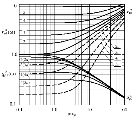
Eqs. (79) and (80). The curves
and are plotted
in Fig. 1 for different values of the nonuniformity parameter
.
Two curves 1 corresponding to the uniform junction () are
fully the same as those shown in Fig. 23 of Chapter 2 in a book by Sze SMS1981 .
The cross-sectional nonuniformity () changes the curves
and in different ways.
The function always and it decreases with growing
regardless of the sign of , as shown by solid
curves in Fig. 1. By contrast, the function
increases for
(solid curves ) and decreases for
(dashed curves ) with growing ,
as compared to curve 1 (for ).
Figure 2: Frequency dependencies of the quantities
and for different values of the nonuniformity
parameter (solid curves 1), (solid curves 2),
1 (solid curves 3), 2 (solid curves 4), 3 (solid curves 5);
(dashed curve ), (dashed curve ),
(dashed curve ), (dashed curve ).
At low frequencies such that and
, the functions
and take
constant values
Then, the factors (79) and (80) become
frequency-independent and equal to
(83)
(84)
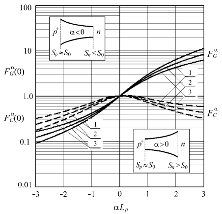
The dependence of the low-frequency factors (83) and (84)
on the nonuniformity parameter is shown in Fig. 2 for three
ratios . Such small values of
are chosen to ensure the condition for neglecting
recombination processes in the depletion layer of width SMS1981 .
Character of the cross-sectional nonuniformity (for with
and for with ) exerts different
influence on (or the conductance
) and on
(or the capacitance ).
The dashed curves in Fig. 2 demonstrate that the low-frequency capacitance
for nonuniform structures (with ) is
always less than for uniform ones (with ) for
both signs and . But the low-frequency conductance
depicted by solid curves increases for
(when ) and decreases for (when ).
Figure 3: Low-frequency values of the factors
(solid curves) and (dashed curves) versus the
nonuniformity parameter for three values of the ratio
(curves 1), (curves 2), (curves 3).
The left and right inserts qualitatively show the longitudinal
geometry of a nonuniform structure with and .
In conclusion, it is pertinent to note that the initial differential
equations (18) and (19) have been solved by using
the exponential approximation for the cross-sectional
-dependence. In this case, the sought eigenfunctions are of exponential
form and
to yield the general solutions (26) and (27).
If the power approximation is more suitable,
Eqs. (18) and (19) can be reduced
to the following form (with or
):
whose solution is (see formula 8.494.9 in Ref. GR1980 )
(85)
where is the Bessel function of the first or second kind.
For equations (18) and (19) we have and
, where is defined by Eq. (22). Therefore,
the sought solutions (26) and (27) include,
instead of the exponential functions, the new functions (85)
dependent on the complex argument .
VII Conclusion
The paper has demonstrated how to derive the explicit analytic form for
the current–voltage characteristics of the PN-junctions with
nonuniformity in the cross section and doping impurity distribution
by applying the transverse averaging technique (TAT).
Application of the TAT to the three-dimensional transport equations
of semiconductor electronics has converted them into the quasi-1D diffusion
equations (13) and (14) to analyze the
minority-carrier transport processes in the nonuniform PN-junctions.
Application of the spectral approach to the quasi-1D diffusion transport
equations for the nonuniform PN-junctions under the action of
arbitrary signal amplitude has given rise to changes in both the static
current–voltage characteristic and the dynamic characteristics
— the diffusion conductance and capacitance ,
as compared with the conventional theory of uniform junctions SMS1981 .
These changes are caused by both factors — the signal amplitude
and the nonuniformity of .
The large-signal effects on the static and dynamic characteristics have
proved to be completely identical to those obtained theoretically and
corroborated experimentally for the uniform PN-junctions
in our previous papers BS2007a ; SB2002 . As a next step, these
results should be compared to simulation.
The influence of the cross-sectional nonuniformity on the static
current–voltage characteristic (53) is exhibited
in terms of the saturation current (54). The similar influence
on the diffusion conductance and capacitance
is demonstrated by the novel formulas (68)–(69)
and (77)–(78). The numerical calculations have been
made for the exponential approximation of the
cross-sectional -dependence.
Until now, large-signal and high-frequency were treated separately to the
best of our knowledge. This study may also have an impact in the understanding
of distortion in high frequency circuits. Further applications, limitations
of the model, carrier storage effects are the focus of further work.
Acknowledgment
One of the authors, AAB, thanks CNPq for
the support during his stay at UFPE.
References
(1) B. Schmithüsen, A. Schenk, I. Ruiz, and W. Fichtner,
“Simulation of physical semiconductor devices under large and small
signal conditions”, (invited paper), Asia Pacific Microwave Conference -
APMC, New Delhi (2004).
(2) A. T. Yang, Y. Liu, and J. T. Yao,
“An efficient nonquasi-static diode model for circuit simulation”,
IEEE Trans. on CAD of Integ. Circ. and Sys., 13, 231–239 (1994).
(3) R. B. Darling,
“A full dynamic model for PN-junction diode switching transients”,
IEEE Trans. on Elect. Dev., bf 42, 969–976 (1995).
(4) D. E. Root, M. Pirola, S. Fan, W. J. Anklam, and A. Cognata,
“Measurement-Based Large-Signal Diode Modeling System for Circuit Device
Design”,
IEEE Trans. on Microwave Theory and Techniques, 41, 2211–2217 (1993).
(5) A. A. Barybin and E. J. P. Santos, “ Transverse averaging
technique for the depletion capacitance of nonuniform PN-junctions”,
Semicond. Sci. Technol. 22 (2007) 312-319.
(6) E. J. P. Santos and A. A. Barybin, “Large-signal
dynamic admittance of -junctions”, Proc. of the
XVII Int. Symp. on Microelectronics Technology and Devices,
Electrochem. Soc. Proc., PV2002-8 (2002) 237-243.
“Novel Results on the Large-Signal Dynamic Admittance of -Junctions”,
cond-mat/0204620.
(7) E. Gatard, R. Sommet, P. Bouysse, R. Quéré,
M. Stanislawiak, J.-M. Bureau,
“High Power S Band Limiter Simulation with a Physics-Based Accurate PIN
Diode Model”
Proceedings of the 2nd European Microwave Integrated Circuits Conference,
Munich, 8 to 10 October 2007.
(8) S. M. Sze, Physics of Semiconductor Devices,
2nd ed. New York: Wiley, 1981.
(9) A. A. Barybin and E. J. P. Santos, “Unified Approach to the
Large-Signal and High-Frequency Theory of PN-Junctions”,
Semicond. Sci. Technol. 22 (2007) 1225-1231.
(10) I. S. Gradshteyn and I. M. Ryzhik, Tables of Integrals,
Series, and Products. New York: Academic Press, 1980.
(11) A. A. Barybin,
Waves in Thin-Film Semiconductor Structures
with Hot Electrons. Moscow: Nauka, 1986 (in Russian).