A singlet triplet hole spin qubit in planar Ge
2L-NESS, Physics Department, Politecnico di Milano, via Anzani 42, 22100, Como, Italy
3Department of Physics, University of Konstanz, D-78457 Konstanz, Germany
4Catalan Institute of Nanoscience and Nanotechnology (ICN2), CSIC and BIST, Campus UAB, Bellaterra, Barcelona, Catalonia, Spain
5ICREA, Passeig de Lluís Companys 23, 08010 Barcelona, Catalonia, Spain
)
Abstract
Spin qubits are considered to be among the most promising candidates for building a quantum processor 1. Group IV hole spin qubits have moved into the focus of interest due to the ease of operation and compatibility with Si technology 2; 3; 4; 5; 6. In addition, Ge offers the option for monolithic superconductor-semiconductor integration. Here we demonstrate a hole spin qubit operating at fields below , the critical field of Al, by exploiting the large out-of-plane hole -factors in planar Ge and by encoding the qubit into the singlet-triplet states of a double quantum dot 7; 8. We observe electrically controlled g-factor-difference-driven and exchange-driven rotations with tunable frequencies exceeding 100 MHz and dephasing times of which we extend beyond with echo techniques. These results demonstrate that Ge hole singlet-triplet qubits are competing with state-of-the art GaAs and Si singlet-triplet qubits. In addition, their rotation frequencies and coherence are on par with Ge single spin qubits, but they can be operated at much lower fields underlining their potential for on chip integration with superconducting technologies.
Holes in Ge have emerged as one of the most promising spin qubit candidates 6 because of their particularly strong spin orbit coupling (SOC) 10, which leads to record manipulation speeds 11; 12, and low dephasing rates 12. In addition, the SOC together with the low effective mass 13 relax fabrication constrains, and larger quantum dots can be operated as qubits without the need for microstrips and micromagnets. In only three years a single Loss-DiVincenzo qubit 14, 2-qubit and most recently even 4-qubit devices have been demonstrated 15; 16; 4. Here we show that by implementing Ge hole spin qubits in a double quantum dot (DQD) device they have the further appealing feature that operation below the critical field of aluminium becomes possible.
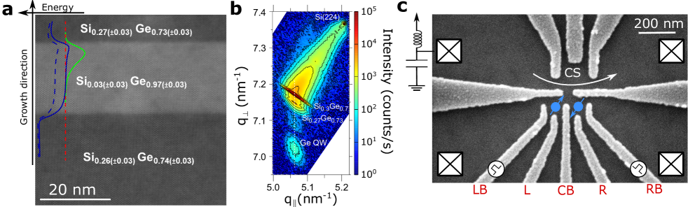
In order to realize such a qubit a strained Ge quantum well (QW) structure, with a hole mobility of at a density of , was grown by low-energy plasma-enhanced chemical vapor deposition (LEPECVD). Starting from a Si wafer a thick strain-relaxed Si0.3Ge0.7 virtual substrate (VS) is obtained by linearly increasing the Ge content during the epitaxial growth. The thick strained Ge QW is then deposited and capped by of Si0.3Ge0.7. In Fig. 1a we show the aberration corrected (AC) high-angle annular dark-field scanning transmission electron microscopy (HAADF-STEM) image of our heterostructure. The HAADF Z-contrast clearly draws the sharp interfaces between the QW and the top and bottom barriers. In addition, x-ray diffraction (XRD) measurements highlight the lattice matching between the virtual substrate and the QW (Fig. 1b). Holes confined in such a QW are of mainly heavy-hole (HH) type because compressive strain and confinement move light-holes (LHs) to higher hole energies 17. The related Kramers doublet of the spin states therefore resembles an effective spin-1/2 system, and .
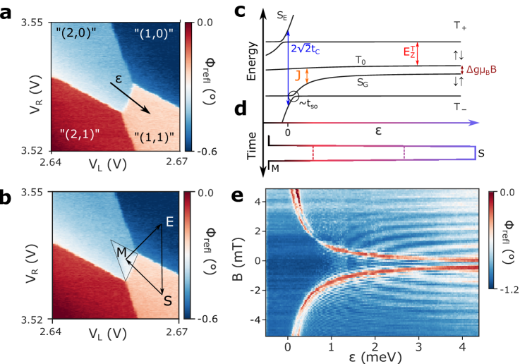
In a singlet-triplet qubit the logical quantum states are defined in a 2-spin 1/2 system with total spin along the quantization axis 7; 8. This is achieved by confining one spin in each of two tunnel coupled quantum dots, formed by depletion gates (Fig. 1c). We tune our device into the single hole transport regime, as shown by the stability diagram in Fig. 2a where the sensor dot reflected phase signal () is displayed as a function of the voltage on L and R (see Methods and Supplementary Fig. S7 and S8). Each Coulomb blocked region corresponds to a fixed hole occupancy, and is labeled by (, ), with () being the equivalent number of holes in the left (right) quantum dot; interdot and dot-lead charge transitions appear as steep changes in the sensor signal. Fast pulses are applied to the outer barrier gates LB and RB which eases pulse calibration since the cross capacitance to the opposite dot is negligible. By pulsing in a clockwise manner along the E-S-M vertices (Fig. 2b) we observe a triangular region leaking inside the upper-left Coulomb blocked region. Such a feature identifies the metastable region where Pauli spin blockade (PSB) occurs: once initialized in E (‘empty’), the pulse to S loads a charge and the spins are separated forming either a spin singlet or a triplet. At the measurement point M within the marked triangle, the spin singlet state leads to tunnel events, while the triplet states remain blocked, which allows spin-to-charge conversion. We repeat the experiment with a counter-clockwise ordering (E-M-S) and no metastable region is observed, as expected (Fig. 2a was acquired while pulsing in the counter-clockwise ordering). We thus consider the interdot line across the detuning () axis of Fig. 2a equivalent to the effective charge transitions. The system is tuned along the detuning axis from (2,0) to (1,1) by applying opposite pulses of amplitude on LB and RB: (see Supplementary Fig. S7), where is the rf-lever arm of the left (right) barrier gate. The DQD spectrum for a finite B field is reported in Fig. 2c (the triplet states T(2,0) lie high up in energy and are not shown; the model Hamiltonian is derived in Supplementary section 1). We set at the crossing. Starting from (2,0) increasing mixes (2,0) and (1,1) into two molecular singlets; the ground state and the excited state , neglected in the following, which are split at resonance by the tunnel coupling . The triplet states are almost unaffected by changes in . We define the exchange energy as the energy difference between and the unpolarized triplet . At large positive detuning drops due to the decrease of the wavefunction overlap for the two separated holes; importantly, different g-factors for the left () and the right dot () result in four (1,1) states: two polarized triplets , and two anti-parallel spin states , split by , where , is the Bohr magneton and is the magnetic field applied in the out-of-plane direction. However, as noticed later, even at large positive a residual persists, which leads to the total energy splitting between and being .
By applying a pulse with varying (Fig. 2d) and stepping the magnetic field we obtain the plot in Fig. 2e drawing a funnel. The experiment maps out the degeneracy between and , where is the Zeeman energy of the polarized triplets and . The doubling of the degeneracy point can be attributed to fast spin-orbit induced oscillations 18. At larger detuning oscillations become visible.
The effective Hamiltonian of the qubit subsystem is:
| (1) |
in the basis, with being the detuning-dependent exchange energy, common to all qubits. Implementations of qubits in GaAs typically harvest the local field gradient induced by the nuclear overhauser field to drive oscillations 8; 19. Due to the near absence of nuclear spins in Si, only slow oscillations could be achieved in natural Si/SiGe structures 20. Hence, micromagnets have been successfully used to enhance and stabilize the magnetic field gradient 21; 22. In Si metal-oxide-semiconductor devices oscillations can be driven by spin-orbit induced g-factor differences in the two dots 23; 24 and values of have been reported. Here, similarly, we realize oscillations through g-factor differences. However, we expect a larger since our holes are of mainly HH character 25; 26. Indeed, as shown below, g-factor differences exceeding can be obtained. Pulsing on influences and the ratio between and determines the rotation axis tilted by an angle from the Z-axis. For large detuning corresponding to X-rotations while for small detuning enabling Z-rotations.
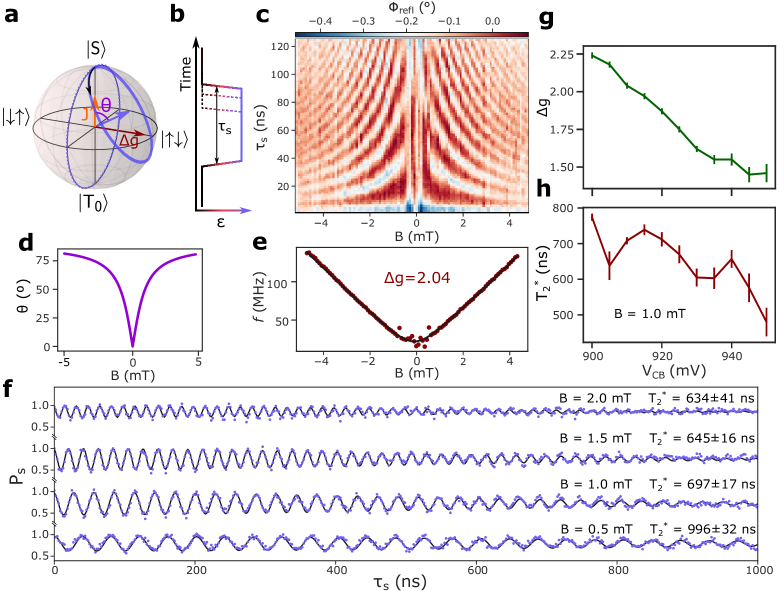
A demonstration of coherent -driven rotations at a center barrier voltage is depicted in Fig. 3c with the pulse sequence shown in Fig. 3b. The system is first initialized in (2,0) in a singlet, then pulsed quickly deep into (1,1) where the holes are separated. Here the state evolves in a plane tilted by (Fig. 3a, Fig. 3d). After a separation time the system is brought quickly to the measurement point in (2,0) where PSB enables the distinction of triplet and singlet. Varying produces sinusoidal oscillations with frequency (Fig. 3e), where is the Planck constant. We extract and . We attribute the large to the different QD sizes which
directly affects the HH-LH splitting determining thus the effective g-factor 17. In addition, the different QD charge occupation can lead to further g-factor differences 25; 28 We approach frequencies of at fields as low as . We observed similar values of in the range of 1.0 to 2.7 in two additional devices with similar gate geometries (see supplementary Fig. S13 ). Fig. 3f shows the extracted singlet probability at different magnetic fields. The black solid line is a fit to , where is the inhomogeneous dephasing time. only oscillates between 0.5 and 1 as a direct consequence of and the tilted rotation axis. One would expect an increase in the oscillation amplitude with higher magnetic field. However, at large the state quickly decays to the singlet during read-out due to relaxation processes 27, reducing the visibility as is clearly shown by the curve at in Fig. 3f. This can be circumvented by different read-out schemes such as latching 29 or shelving 30 but this is out of the scope of the present work, which focuses on the low magnetic field behavior.
We, furthermore, observe a dependence of on the voltage on CB (Fig. 3g) confirming electrical control over the -factors. As the voltage is decreased by , varies from to more than 2.2 which conversely increases the frequency of X-rotations. Concurrently we measure a similar trend in reported at in Fig. 3h; as the center barrier is lowered the coherence of the qubit is enhanced. The origin and consequences of this observation are discussed later.
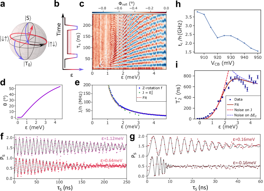
Next, we demonstrate full access to the Bloch sphere achieved by Z-rotations leveraging the exchange interaction. We change the pulse sequence (Fig. 4b) such that after initialization in a singlet the system is pulsed to large detuning but is maintained in this position only for corresponding to a rotation, bringing the system close to . Now we let the state evolve for a time at a smaller detuning, increasing and changing the rotation angle (Fig. 4d), before applying another rotation at high detuning and pulsing back to read-out. The state evolution on the Bloch sphere in Fig. 4a shows that full access to the qubit space can be obtained by a combination of appropriately timed pulses. The resulting oscillation pattern is depicted in Fig. 4c. From the inferred frequency we find the dependence of on and extract as a free fitting parameter. The extracted values of are plotted in Fig. 4e with the blue markers obtained from the exchange oscillation frequency. The green dots, on the other hand, correspond to extracted from the funnel experiment (Fig. 2e). We find that the two sets of data points coincide when . Together with the g-factor difference already reported we obtain the two out-of-plane g-factors to be and , comparable to previous studies 26.
In Fig. 4f and g we plot as a function of separation time at different values of . now oscillates between 0 and 1 due to the combination of -pulses and free evolution time at lower detuning.
From the fits (black solid lines) at different detunings we extract as a function of (Fig.4i). For low the coherence time is shorter than , while it increases for larger and saturates at around . This is explained by a simple noise model 19; 21 where depends on electric noise on and a combination of electric and magnetic noise affecting :
| (2) |
where is the rms noise on detuning, describes the combination of electric noise on and magnetic noise affecting . We assume as we observe almost no change in with detuning (see Supplementary Fig. S9). From the fit (dark red solid line) we find , in line with comparable experiments 19; 21, and . Although is much smaller than we find that at large detuning coherence is still limited by noise on because (see red and violet dashed lines in Fig. 4i). We attribute the magentic noise to randomly fluctuating hyperfine fields caused by spin-carrying isotopes in natural Ge but a distinction from charge noise affecting can not be made here. Eq. (2) also gives insight into the trends observed in Fig. 3f and h. With we now affect and, thereby, its contribution to the total energy. The higher the ratio the more the coherence is limited by this term as confirmed by the drop in with magnetic field in Fig. 3f. Similarly one would expect that by increasing , should be lower. But, as shown in Fig. 4h, the raising g-factor difference is accompanied by an increase of the tunnel coupling by . Hence, is larger at lower and is reduced leading to a longer . While affects both and , we see that and affect mostly and leave unaltered (see Supplementary Fig. S10). This exceptional tunability enables electrical engineering of the potential landscape to favor fast operations without negatively affecting the coherence times, thus enhancing the quality factor of this qubit. We find a quality factor that increases with magnetic field reaching at (see Supplementary Fig. S15). While the longest reported here is already comparable to electron singlet-triplet qubits in natural Si 22, a reduction in the magnetic noise contribution by isotopic purification could further improve qubit dephasing and quality 23; 24.
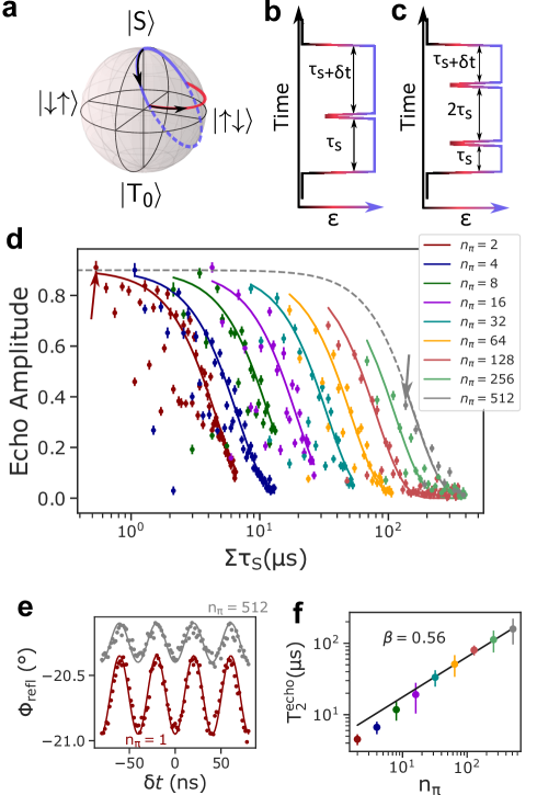
We now focus on extending the coherence of the qubit by applying refocusing pulses similar to those developed in nuclear magnetic resonance (NMR) experiments. We investigate the high region where charge noise on detuning is lowest. Exchange pulses at are adopted as refocusing pulses. We note, however, that to obtain a perfect correcting pulse, it would be necessary to implement a more complex pulse scheme 31. We choose convenient values () such that, if no decoherence has occurred, the system will always be found in the same state after . The refocusing pulse is then calibrated to apply a -pulse that brings the state on the same trajectory as before the refocusing pulse (Fig. 5a and Supplementary Fig. S16). The free evolution time after the last refocusing pulse is varied in length from to (Fig. 5b,c) and we observe the amplitude of the resulting oscillations (Fig. 5e). Also, we increase the number of applied pulses from to , thereby increasing the total free evolution time of the qubit and performing a Carr-Purcell-Meiboom-Gill echo. The decay is fit to a Gaussian decay and we extract a of for and for , the longest reported so far in this material. Furthermore, we observe a power law dependence of as a function of the number of refocusing pulses and find with suggesting a limitation by low frequency noise 32. We note that for we extract being a signature of quasi-static noise with spectral density .
In conclusion we have shown coherent 2-axis control of a hole singlet-triplet qubit in Ge with an inhomogeneous dephasing time of at .
We have taken advantage of an intrinsic property of heavy hole states in Ge, namely their large and electrically tunable out-of-plane g-factors. We achieved electrically driven -rotations of at fields of only . Compared to driven singlet-triplet qubits in isotopically purified Si metal-oxide-semiconductor structures 23; 24 we find a g-factor difference that is 3 orders of magnitude larger. Moreover, we demonstrate an electrical tunability of the g-factor difference ranging from 50% to more than 200% over a gate range of in different devices. The large g-factor differences were confirmed in 2 additional devices underlining the reproducibility of the Ge platform.
Echo sequences revealed a noise spectral density dominated largely by low frequency noise. The results and progress of singlet-triplet qubits, especially in the GaAs platform, will largely be applicable in Ge as well. Real time Hamiltonian estimation 33 can boost , a deeper understanding of the noise mechanisms might result in prolonging coherence even further 34 and feedback controlled gate operation could push gate fidelity beyond the threshold for fault tolerant computation 35.
In the future, latched or shelved read-out could circumvent the decay of to singlet during read-out opening the exploration of the qubit’s behavior at slightly higher magnetic fields where the -rotation frequencies could surpass the highest electron-dipole spin-resonance Rabi frequencies reported so far 11; 12, without suffering from reduced dephasing times. Furthermore, by moving towards symmetric operation or resonant driving the quality of exchange oscillations can be increased since the qubit is operated at an optimal working point 36; 37; 38; 22. The operation of Ge qubits at very low fields can further improve their prospects in terms of scalability and high fidelity fast readout, as it will facilitate their integration with superconducting circuits such as Josephson parametric amplifiers, superconducting resonators and superconducting quantum interference devices 39; 40; 41; 42; 43; 44
The long coherence times combined with fast and simple operations at extremely low magnetic fields make this qubit an optimal candidate for integration into a large scale quantum processor.
Methods
Quantum well growth:
In contrast with Ge QWs previously employed for qubit fabrication 6, in the present study the strained Ge QW structure was grown by low-energy plasma-enhanced chemical vapor deposition (LEPECVD) 45 instead of thermal CVD. The buffer between the Si(001) wafer and the Ge QW structure is a graded region approximately thick in which the Ge content was increased linearly from pure Si up to the desired final composition of Si0.3Ge0.7. Thermal CVD grown buffers typically exploit a reverse-graded approach starting from a thick pure-Ge layer on the Si(001) wafer 46. As a consequence the Ge content in the SiGe spacers used here is approximately 70 %, a lower value than the 80 % used in previous reports.
This will induce larger strain in the Ge QW 47 and therefore a larger energy difference between HH and LH states, an important feature in order to engineer as pure as possible HH states with large out of plane g-factors and g-factor differences. In the case of Ge QWs grown by thermal CVD on reverse-graded buffers, the buffer and SiGe spacers tend to display a small residual tensile strain 48.
The substrate temperature was reduced from 760 to 550∘C with increasing Ge content. The buffer was completed with a region at a constant composition of Si0.3Ge0.7. This part is concluded in about , with a growth rate of 5- due to the efficient dissociation of the precursor gas molecules by the high-density plasma. The graded VS typically presents a threading dislocation density of about 49. The substrate temperature and plasma density was then reduced without interrupting the growth. The undoped Si0.3Ge0.7/Ge/Si0.3Ge0.7 QW stack was grown at and a growth rate of about to limit Si intermixing and interface diffusion. A Si cap was deposited after a short () interruption to facilitate the formation of the native oxide (the interruption reduces Ge contamination in the Si cap from residual precursor gases in the growth chamber). SIMS analysis indicates that boron levels are below the detection limit of to a depth of at least .
Device fabrication: The samples were processed in the IST Austria Nanofabrication Facility. A chip is cut out from a 4 inch wafer and cleaned before further processing. The Ohmic contacts are first patterned in a electron beam lithography system, then a few of native oxide and the SiGe spacer is milled down by argon bombardment and subsequently a layer of 60 Pt is deposited in situ under an angle of , to obtain reproducible contacts. No additional intentional annealing is performed. A mesa of is etched in a reactive ion etching step. The native SiO2 is removed by a dip in buffered HF before the gate oxide is deposited. The oxide is a ALD aluminum oxide (Al2O3) grown at , which unintentionally anneals the Ohmic contacts resulting in a low resistance contact to the carriers in the quantum well. The top gates are first patterned via ebeam lithography and then a Ti/Pd 3/27 layer is deposited in an electron beam evaporator. The thinnest gates are 30 wide and 30 apart. An additional thick gate metal layer is subsequently written and deposited and serves to overcome the Mesa step and allow wire bonding of the sample without shorting gates together. Quantum dots are formed by means of depletion gates (Fig. 1c). The lower gates (LB, L, CB, R, RB) form a double quantum dot (DQD) system and the upper gates tune a charge sensor (CS) dot. The separation gates in the middle are tuned to maximize the CS sensitivity to charge transitions in the DQD. An LC-circuit connected to a CS ohmic contact allows fast read-out through microwave reflectometry. LB and RB are further connected to fast gate lines enabling fast control of the energy levels in the DQD.
ACKNOWLEDGMENTS This research was supported by the Scientific Service Units of IST Austria through resources provided by the MIBA Machine Shop and the nanofabrication facility and was made possible with the support of the NOMIS Foundation. This project has received funding from the European Union’s Horizon 2020 research and innovation program under the Marie Sklodowska-Curie grant agreement No. 844511, No. 75441, and by the FWF-P 30207 project. A.B. acknowledges support from the EU Horizon-2020 FET project microSPIRE, ID: 766955. M.B. and J.A. acknowledge funding from Generalitat de Catalunya 2017 SGR 327. ICN2 is supported by the Severo Ochoa program from Spanish MINECO (Grant No. SEV-2017-0706) and is funded by the CERCA Programme / Generalitat de Catalunya. Part of the present work has been performed in the framework of Universitat Autònoma de Barcelona Materials Science PhD program. Part of the HAADF-STEM microscopy was conducted in the Laboratorio de Microscopias Avanzadas at Instituto de Nanociencia de Aragon-Universidad de Zaragoza. ICN2 acknowledge support from CSIC Research Platform on Quantum Technologies PTI-001. M.B. acknowledges funding from AGAUR Generalitat de Catalunya FI PhD grant.
DATA AVAILABILITY All data included in this work will be available from the IST Austria repository.
Author Contributions
D.J. fabricated the sample, performed the experiments and data analysis. D.J., A.H and I.P. developed the fabrication recipe. D.J., A.H, O.S. and M. Bor. performed pre-characterizing measurements on equivalent samples. J.S.M. and G.K. fabricated the two additional devices discussed in the supplementary information. J.K. performed the experiments on those additional devices. D.C. and A.B. designed the SiGe heterostructure. A.B. performed the growth supervised by G. I.. D.C. performed the x-ray diffraction measurements and simulations.
G.T. performed Hall effect measurements, supervised by D.C..
P.M.M. derived the theoretical model. M.Bot. and J.A. performed the atomic resolution (S)TEM structural and EELS compositional related characterization and calculated the strain by using GPA. D.J., A.H., J.K, A.C., F.M., J.S.M and G.K. discussed the qubit data. D.J. and G.K. wrote the manuscript with input from all the authors. G.I. and G.K. initiated and supervised the project.
References
- 1 Vandersypen, L. M. K. et al. Interfacing spin qubits in quantum dots and donors—hot, dense, and coherent. npj Quantum Information 3 (2017).
- 2 Maurand, R. et al. A CMOS silicon spin qubit. Nature Communications 7 (2016).
- 3 Crippa, A. et al. Gate-reflectometry dispersive readout and coherent control of a spin qubit in silicon. Nature Communications 10 (2019).
- 4 Hendrickx, N. W., Franke, D. P., Sammak, A., Scappucci, G. & Veldhorst, M. Fast two-qubit logic with holes in germanium. Nature 577, 487–491 (2020).
- 5 Kobayashi, T. et al. Engineering long spin coherence times of spin–orbit qubits in silicon. Nature Materials (2020).
- 6 Scappucci, G. et al. The germanium quantum information route. arXiv: 2004.08133 [cond-mat], Nature Review Materials (accepted) (2020).
- 7 Levy, J. Universal quantum computation with spin-1/2pairs and heisenberg exchange. Physical Review Letters 89 (2002).
- 8 Petta, J. R. Coherent manipulation of coupled electron spins in semiconductor quantum dots. Science 309, 2180–2184 (2005).
- 9 Amitonov, S. V., Spruijtenburg, P. C., Vervoort, M. W. S., van der Wiel, W. G. & Zwanenburg, F. A. Depletion-mode quantum dots in intrinsic silicon. Applied Physics Letters 112, 023102 (2018).
- 10 Kloeffel, C., Trif, M. & Loss, D. Strong spin-orbit interaction and helical hole states in Ge/Si nanowires. Physical Review B 84 (2011).
- 11 Froning, F. N. M. et al. Ultrafast hole spin qubit with gate-tunable spin-orbit switch. arXiv: 2006.11175 [cond-mat] (2020).
- 12 Wang, K. et al. Ultrafast operations of a hole spin qubit in ge quantum dot. arXiv: 2006.12340 [cond-mat] (2020).
- 13 Lodari, M. et al. Light effective hole mass in undoped Ge/SiGe quantum wells. Physical Review B 100 (2019).
- 14 Loss, D. & DiVincenzo, D. P. Quantum computation with quantum dots. Physical Review A 57, 120–126 (1998).
- 15 Hendrickx, N. W. et al. A four-qubit germanium quantum processor. arXiv: 2009.04268 [cond-mat] (2020).
- 16 Watzinger, H. et al. A germanium hole spin qubit. Nature Communications 9 (2018).
- 17 Katsaros, G. et al. Observation of spin-selective tunneling in SiGe nanocrystals. Physical Review Letters 107 (2011).
- 18 Petta, J. R., Lu, H. & Gossard, A. C. A coherent beam splitter for electronic spin states. Science 327, 669–672 (2010).
- 19 Dial, O. E. et al. Charge noise spectroscopy using coherent exchange oscillations in a singlet-triplet qubit. Physical Review Letters 110 (2013).
- 20 Maune, B. M. et al. Coherent singlet-triplet oscillations in a silicon-based double quantum dot. Nature 481, 344–347 (2012).
- 21 Wu, X. et al. Two-axis control of a singlet-triplet qubit with an integrated micromagnet. Proceedings of the National Academy of Sciences 111, 11938–11942 (2014).
- 22 Takeda, K., Noiri, A., Yoneda, J., Nakajima, T. & Tarucha, S. Resonantly driven singlet-triplet spin qubit in silicon. Physical Review Letters 124 (2020).
- 23 Jock, R. M. et al. A silicon metal-oxide-semiconductor electron spin-orbit qubit. Nature Communications 9 (2018).
- 24 Harvey-Collard, P. et al. Spin-orbit interactions for singlet-triplet qubits in silicon. Physical Review Letters 122 (2019).
- 25 Watzinger, H. et al. Heavy-hole states in germanium hut wires. Nano Letters 16, 6879–6885 (2016). URL https://doi.org/10.1021/acs.nanolett.6b02715.
- 26 Hofmann, A. et al. Assessing the potential of Ge/SiGe quantum dots as hosts for singlet-triplet qubits. arXiv: 1910.05841 [cond-mat] (2019).
- 27 Barthel, C. et al. Relaxation and readout visibility of a singlet-triplet qubit in an overhauser field gradient. Physical Review B 85 (2012).
- 28 Liles, S. D. et al. Spin and orbital structure of the first six holes in a silicon metal-oxide-semiconductor quantum dot. Nature Communications 9, 3255 (2018).
- 29 Studenikin, S. A. et al. Enhanced charge detection of spin qubit readout via an intermediate state. Applied Physics Letters 101, 233101 (2012).
- 30 Orona, L. A. et al. Readout of singlet-triplet qubits at large magnetic field gradients. Physical Review B 98 (2018).
- 31 Wang, X. et al. Composite pulses for robust universal control of singlet–triplet qubits. Nature Communications 3 (2012).
- 32 Yoneda, J. et al. A quantum-dot spin qubit with coherence limited by charge noise and fidelity higher than 99.9%. Nature Nanotechnology 13, 102–106 (2017).
- 33 Shulman, M. D. et al. Suppressing qubit dephasing using real-time Hamiltonian estimation. Nature Communications 5 (2014).
- 34 Bluhm, H. et al. Dephasing time of GaAs electron-spin qubits coupled to a nuclear bath exceeding 200 s. Nature Physics 7, 109–113 (2010).
- 35 Cerfontaine, P. et al. Closed-loop control of a GaAs-based singlet-triplet spin qubit with 99.5% gate fidelity and low leakage. Nature Communications 11 (2020).
- 36 Martins, F. et al. Noise suppression using symmetric exchange gates in spin qubits. Physical Review Letters 116 (2016).
- 37 Reed, M. et al. Reduced sensitivity to charge noise in semiconductor spin qubits via symmetric operation. Physical Review Letters 116 (2016).
- 38 Nichol, J. M. et al. High-fidelity entangling gate for double-quantum-dot spin qubits. npj Quantum Information 3 (2017).
- 39 Wallraff, A. et al. Strong coupling of a single photon to a superconducting qubit using circuit quantum electrodynamics. Nature 431, 162–167 (2004).
- 40 Stehlik, J. et al. Fast charge sensing of a cavity-coupled double quantum dot using a josephson parametric amplifier. Physical Review Applied 4 (2015).
- 41 Burkard, G., Gullans, M. J., Mi, X. & Petta, J. R. Superconductor–semiconductor hybrid-circuit quantum electrodynamics. Nature Reviews Physics 2, 129–140 (2020).
- 42 Leonard, E. et al. Digital coherent control of a superconducting qubit. Physical Review Applied 11 (2019).
- 43 Schupp, F. J. et al. Sensitive radiofrequency readout of quantum dots using an ultra-low-noise SQUID amplifier. Journal of Applied Physics 127, 244503 (2020).
- 44 Vigneau, F. et al. Germanium quantum-well Josephson field-effect transistors and interferometers. Nano Letters 19, 1023–1027 (2019).
- 45 Rössner, B., Chrastina, D., Isella, G. & von Känel, H. Scattering mechanisms in high-mobility strained Ge channels. Applied Physics Letters 84, 3058–3060 (2004).
- 46 Shah, V. A. et al. Reverse graded relaxed buffers for high Ge content SiGe virtual substrates. Applied Physics Letters 93, 192103 (2008). URL https://doi.org/10.1063/1.3023068. https://doi.org/10.1063/1.3023068.
- 47 Wang, Z. et al. Suppressing charge-noise sensitivity in high-speed Ge hole spin-orbit qubits. arXiv: 1911.11143 [cond-mat] (2019).
- 48 Sammak, A. et al. Shallow and undoped germanium quantum wells: A playground for spin and hybrid quantum technology. Advanced Functional Materials 29, 1807613 (2019).
- 49 Marchionna, S., Virtuani, A., Acciarri, M., Isella, G. & von Kaenel, H. Defect imaging of SiGe strain relaxed buffers grown by LEPECVD. Materials Science in Semiconductor Processing 9, 802–805 (2006).