ignore
Field Trial of a Flexible Real-time Software-defined GPU-based Optical Receiver
Abstract
We introduce a flexible, software-defined real-time multi-modulation format receiver implemented on an off-the-shelf general-purpose graphics processing unit (GPU). The flexible receiver is able to process 2 GBaud 2-, 4-, 8-, and 16-ary pulse-amplitude modulation (PAM) signals as well as 1 GBaud 4-, 16- and 64-ary quadrature amplitude modulation (QAM) signals, with the latter detected using a Kramers-Kronig (KK) coherent receiver. Experimental performance evaluation is shown for back-to-back. In addition, by using the JGN high speed R&D network testbed, performance is evaluated after transmission over 91 km field-deployed optical fiber and reconfigurable optical add-drop multiplexers (ROADMs).
Index Terms:
Real-time, GPU, field trial, Kramers-Kronig.I Introduction
With the continual increase in demand for data-traffic at lower cost-per-bit, there is an increased interest in low-cost optical transceivers for data-center interconnects. Multi-vendor standards, e.g. [1], are key to the development and roll-out of these systems. Software-defined transceivers have supported and enhanced the widespread development of 5G and other wireless communications standards [2]. These systems perform digital signal processing (DSP) wholly [3] or partially [4] using off-the-shelf general purpose hardware, leading to high flexibility, combined with low development effort and rapid turnaround. Therefore, software-defined transceivers are expected to play an increasing role in the rapid development, validation, and test of optical communication standards.
Whilst commonplace for wireless systems, the development of software-defined transceivers for optical communications has been restricted by energy and computing power limitations. Recently, exploiting field-programmable gate arrays (FPGAs) for real-time DSP for optical communications has been investigated [5, 6, 7]. GPU-based systems for optical communications are restricted by energy and computing power to prototype and test. With 45% [8] year-on-year growth of computing power and 25% increase [9] in energy efficiency (FLOPS per Watt), general-purpose GPUs have the potential to meet demanding processing requirements. Note that, GPU power efficiency showed a 3-fold improvement over equivalent FPGA for simple highly-parallelized operations [10]. These exponential increases may facilitate GPU use beyond prototyping. Compared to GPUs, FPGAs require longer development times and more stringent resource management to achieve the specific functions required for DSP.
Recently, the use of general-purpose GPUs has been demonstrated for specific functions such as forward error correction (FEC) decoding [11, 12] and physical-layer functions for optical communications [13, 14, 15]. Additionally, real-time DSP for optical differential quaternary phase-shift-keying (DQPSK) has been implemented on a GPU [16, 17, 18]. In these papers, massive parallel processing capabilities of GPUs were exploited for processing single-polarization DQPSK signals, correcting for intersymbol interference (ISI) using a finite impulse response (FIR) filter. This approach greatly increases flexibility of optical transceivers. However, there remains the potential to further improve on this concept, since single-polarization coherent systems require real-time polarization control and differential phase-shift keyed modulation does not provide high spectral efficiency.
In this work, we implement a flexible, software-defined real-time multi-modulation format receiver. A full real-time DSP chain is implemented on a commercial, off-the-shelf general-purpose GPU and validated experimentally. The receiver DSP uses massive parallelization to receive PAM /̄2, -4, -8, and -16 signals at as well as 4-, 16-, and 64/̄QAM signals at , with the latter detected using a KK coherent receiver[19]. All measurements employ identical transmitter and receiver hardware without polarization control. The GPU software is able to switch between modulation formats. To the authors’ knowledge, this is the first demonstration of a multi-modulation format software-defined GPU-based receiver and the first real-time demonstration of coherent KK detection.
Furthermore, we validate the performance in a optical fiber link over a field-deployed metropolitan network. The fiber ring is part of the Japan Gigabit Network (JGN) high speed R&D network testbed [20] consisting of 3 commercial ROADMs in 2 separate Tokyo locations. These results demonstrate the potential of software-defined receivers for low-cost optical links, exploiting the exponentially growing computing power of GPUs.
This paper is an extension to the work presented at the European Conference on Optical Communications (ECOC) 2020 [21]. Additional results and a detailed description of the structure of the real-time receiver architecture and the algorithms implemented on the GPU are presented. Clock-recovery for intensity-modulation direct-detection (IM/DD) PAM /̄N signals is shown to tolerate rapid changes in clock-frequency offset and static clock-frequency offsets of up to . Using a noise-loading optical setup, PAM /̄2, 4, 8 signals are shown to reach the optical signal-to-noise ratio (OSNR) Q-factor threshold for 6.7% overhead hard decision forward error correction (HD-FEC) [22] at , , and , respectively. After transmission through the field trial network, an OSNR penalty of and is observed for PAM /̄2 and PAM /̄4, respectively. For PAM /̄8, a 20% overhead HD-FEC was necessary since it cannot reach the 6.7% threshold. PAM /̄16 can be decoded in real time both in back-to-back and after transmission using the GPU DSP, but signal quality is not sufficient to reach either HD-FEC threshold. For KK N/̄QAM signals, carrier-to-signal power ratio (CSPR) optimization was performed and a CSPR of was chosen for 4/̄QAM and for 16- and 64/̄QAM. 4- and 16/̄QAM signals reach the 6.7% overhead HD-FEC threshold at OSNR, whilst 16/̄QAM requires an OSNR of for back-to-back and transmission, respectively. 64/̄QAM signals were processed in real time, but performance was not sufficient to reach either HD-FEC threshold. Six second continuous real-time transmission of all modulation formats show stable short-term average Q-factors despite the varying environment of installed fiber.
This paper is structured as follows: Section II introduces GPU processing and the general structure of the real-time GPU receiver architecture. Section III describes the DSP algorithms employed for IM/DD PAM /̄N signals in detail and with performance evaluation the in a back-to-back scenario. Section IV discusses the implementation and back-to-back evaluation for KK N/̄QAM signals. Section V discusses the evaluation of the real-time receiver evaluated using the experimental field trial network. Finally, Section VI concludes this paper.
II Real-time GPU Receiver Architecture
II-A Comparison between FPGA and GPU processing
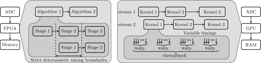
Fig. 1 shows the similarities and differences between FPGA and GPU parallel processing architectures. Data are digitized by an ADC, copied to the processing device, and after processing the results are stored in memory. Timings between parallel stages of processing in FPGAs processing are deterministic and strictly controlled. The FPGA operates at a certain clock rate and every stage of processing should fit within the timing parameters imposed by this central clock. Also, each stage of processing is assigned a fixed portion of physical computing hardware. In contrast, execution times on the GPU are not deterministic. Computing hardware is shared for all kernels and a central scheduler assigns computing resources to kernels running in parallel.
II-B GPU processing terminology
Kernels are highly parallel routines that act upon data in the GPU memory. The GPU code of the kernel is performed by threads running in parallel. A thread is executed on a GPU core and efficient implementations can use millions of threads. A group of 32 threads is called a warp and is guaranteed to execute simultaneously, which allows for very efficient data exchange between these threads through warp-level shuffles, used in this work for certain reduction kernels. A group of warps, called a threadblock, is executed on the same streaming multiprocessor, which is a group of GPU cores. Threads in a threadblock share physical computing hardware and memory, leading to caching benefits. Multiple threadblocks are not necessarily performed in parallel. This depends on the scheduling by the GPU driver.
Dependencies in the signal processing chain need to be handled appropriately. Kernels in the same processing stream are performed in order. Therefore, splitting an algorithm into separate kernels in the same stream can address the dependency. Alternatively, a single threadblock can be employed to perform a certain algorithm, synchronization within a threadblock is possible since it runs the same piece of physical hardware. Kernels in different streams run parallel to each other. In this case, events can be used to halt one stream until a certain kernel in another stream has finished processing.
II-C Continuous real-time processing requirements
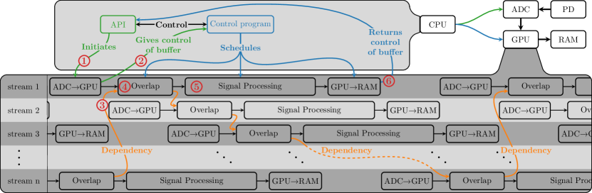
The real-time GPU receiver consists of a photodiode connected to a ADC. Digitized samples are copied in buffers from the ADC to the GPU where they are processed in a highly parallel manner. Each buffer contains 222 samples, which takes at . In our implementation, each buffer is assigned its own processing stream and any dependencies to ensure data continuity are handled by events. For real-time processing, the buffers need to be processed as fast or faster than they are created by the ADC in order to avoid data loss. As such, the average buffer processing time needs to be lower than times the number of streams employed. Therefore, buffer processing times can be relaxed by increasing the number of parallel streams at the expense of increased latency.
II-D GPU signal processing structure
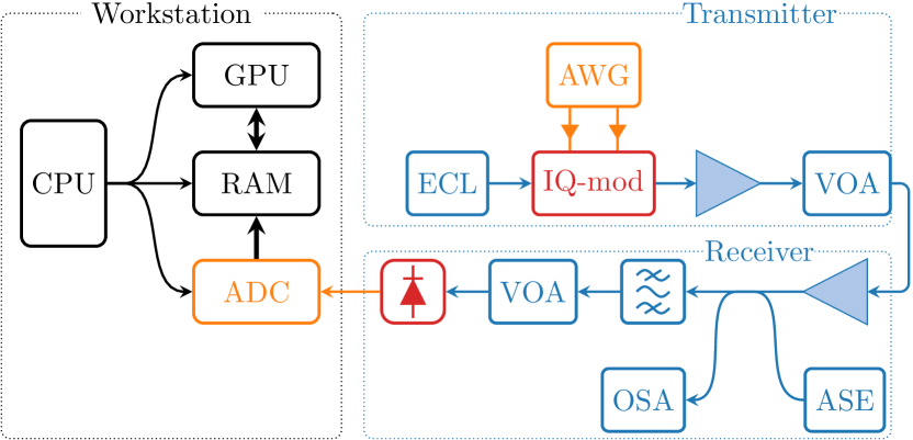
Fig. 2 shows the structure of receiver, the tasks performed by the GPU, and how those are controlled by the CPU. The ADC is controlled by an application programming interface (API), provided by the manufacturer which also manages the data transfer to the GPU. A second program, written by the authors, controls the API and launches signal processing kernels.
-
•
Step 1: The ADC digitizes the analog signal into 12-bit digital samples at either 2 (IM/DD) or 4 (KK) samples per symbol and temporarily stores them in ADC memory. The API initiates the transfer of a buffer containing 222 samples from ADC memory to GPU memory using direct memory access (DMA), provided a free GPU buffer is available for the API to use. This is marked as Step 1 in Fig. 2. Each buffer is assigned its own stream and DSP kernels are added to that stream to process the data.
-
•
Step 2: Control over the GPU buffer which now contains the digitized signal is handed over to the control program written by the authors.
-
•
Step 3: For continuous real-time data processing certain overlap between buffers is required, an overlap kernel is used for this. These overlap kernels need to be executed in order and events ensure an overlap kernel cannot start processing until its predecessor is finished. This is shown in Fig. 2 as Step 3 and marked as Dependency.
-
•
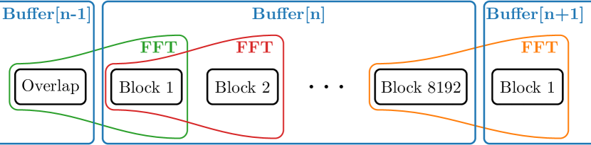
Step 4: The 222 samples in a buffer are subdivided into 8192 blocks of 512 samples for frequency domain (FD) processing as depicted in Fig. 3. FD processing requires one block of overlap between buffers for data continuity. An overlap kernel handles this by prepending a block to the current buffer which was stored elsewhere in memory. Afterwards, it copies the last block of its buffer to memory for the next overlap kernel to use. Also, the overlap kernel converts the data from 12-bit unsigned integers to 32-bit floats.
-
•
Step 5: This step contains the actual DSP chain which uses both time domain (TD) and 100% overlap-save FD processing. This block uses floating point samples as input and produces decoded bits as output. A detailed description can be found in Sections III and IV for PAM /̄N and N/̄QAM signals, respectively.
-
•
Step 6: After processing, the decoded bits are copied to random-access memory (RAM) and control over the buffer is handed back to the API.
III IM/DD GPU Signal Processing Chain
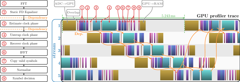
Fig. 4 lists the DSP chain for IM/DD PAM /̄N signals. It consists of 9 steps, each of which executed by one or more kernels. To support real-time operation, five parallel streams are used as shown in the annotated profiler trace in Fig. 4. Dependencies between algorithms running in parallel streams are handled through events which are marked as Dependency in the DSP chain and shown by the orange arrows in the profiler trace.
III-A Step 1 and 2: fast Fourier transform (FFT) and Static Equalization
The IM/DD signal processing chain starts after overlap copying. A 100% overlap-save 1024-point FFT at 2 samples-per-symbol is performed using a readily-available highly-parallel GPU FFT implementation. This splits the 222 samples in the buffer into 8192 blocks of 1024 samples, of which 512 are valid due to 100% overlap-save. Secondly, static FD equalization is performed to compensate for receiver bandwidth impairments using a pre-computed FIR filter. This filter optimized offline in TD using 503 taps, converted to a 1024-point FD version, and uploaded to the GPU. The number of taps was limited to 503 to prevent introduction of ISI through the cyclic nature of the 1024-point FFT.
To fully appreciate the parallel nature of this processing, we need to look at the number of independent threads working in this one kernel alone. FD equalization requires 512 complex multiplications to be performed for each of the 8192 blocks, Hermitian symmetry allows for the omission of half of the spectrum. To this end, 221 threads are launched, each operating on 2 complex samples (4 32-bit floats) at a time. 128-bit vector loads/stores allow for the 4 floats to be loaded/stored using just a single instruction, increasing memory throughput. These 221 threads can be performed in parallel, exploiting the massive parallel capabilities of the GPU. Fig. 4 shows that during the execution of this kernel in stream 1, marked as step 2, is performed in parallel with a ADC-to-GPU copy in stream 2 and other stages of the signal processing of other buffers in streams 4 and 5. Therefore, parallelization is not only exploited within kernels acting on a buffer, but also between streams operating on different buffers.
III-B Step 3 and 4: Clock-phase Estimation and Unwrapping
Clock-phase estimation is performed block-wise in FD after static equalization using a technique introduced in [23]. This provides an estimate clock-phase for each block of samples. To improve noise tolerance, these estimates are averaged over 105 blocks. This requires the 52 previous and 52 future clock-phase estimates to be known as well. The causality issue of the future estimates is resolved through increased buffering in the overlap kernel before actual signal processing starts. The dependency on previous estimates requires the clock-phase estimation of the previous buffer to be completed before the averaging and unwrapping step of the current buffer can be allowed to start. To this end, events are used to signal when clock-phase estimation is completed, allowing for the current processing to wait until the previous has completed. Note that only the estimation step has this dependency, the remainder of the signal processing can occur in parallel. The events resolving these dependencies are shown by orange arrows in Fig. 4.
The clock-phase estimates are restricted to . Hence, averaging is performed through vector addition in complex space and subsequent phase unwrapping is required. It is denoted as step 4 in Fig. 4. The phase unwrapping kernel checks whether the current averaged clock-phase differs more than from the previous. This sequential algorithm is hard to parallelize. To some extent this is done through inter-thread communication using warp-level shuffles. This requires some significant processing time. However, the unwrapping algorithm uses a single warp of 32 threads and leaves much of the GPU processing power unused, which can be used by other kernels running in different streams. For example, during the phase unwrapping in stream 1, stream 2 performs an FFT, FD equalization, and clock-phase estimation, stream 3 performs a ADC-to-GPU memory copy, stream 4 is idle, and stream 5 performs normalization, symbol decision, and a GPU-to-RAM copy. Therefore, phase unwrapping does not take up significant amount of resources, even though it takes up significant amount of time.
III-C Step 5-9: Clock Recovery, IFFT, Normalization, and symbol decision
Clock recovery is performed by correcting for the unwrapped clock-phase in FD. After the 1024-point inverse fast Fourier transform (IFFT), 256 valid symbols need to be extracted for further processing. In the presence of clock-frequency offset, every now and then, either more or fewer symbols may need to be extracted from a block to keep the unwrapped clock-phase within bounds. This is performed in step 7 of Fig. 4, which converts the fixed rate sample input to a variable rate symbol output. Then, buffer-wise normalization is performed using three kernels: initialization, estimation of the DC-offset, and estimation of the amplitude. In the symbol decision kernel, the DC-offset and amplitude are corrected for and PAM /̄N symbols are decoded into bits. Decision thresholds are optimized offline beforehand and uploaded to the GPU.
III-D Experimental setup for back-to-back evaluation of PAM /̄N
Fig. 5 shows a diagram of the experimental setup for back-to-back characterization of the real-time receiver. At the transmitter, the lightwave from a linewidth external cavity laser (ECL) centered at is modulated using a single-polarization in-phase and quadrature modulator (IQM). Electrical driving signals for the IQM are provided by a 2-channel arbitrary-waveform generator (AWG) operating at amplified by RF-amplifiers, whilst bias-tees and voltage sources control the bias of the modulator arms. PAM /̄N signals are modulated by biasing one of the IQM-arms to mid-point and driving it with a baseband 2 Gbaud 50% roll-off root-raised-cosine (RRC) pulse-shaped signal.
The receiver consists of an erbium-doped fiber amplifier (EDFA) pre-amplifier followed by a 0.04 nm bandpass filter (BPF). In addition, a noise-loading setup is included with an amplified spontaneous emission (ASE) source and an optical spectrum analyzer (OSA) through a 22 coupler. A variable optical attenuator (VOA) is used to control the power at the input of a PD with a cut-off frequency of . The electrical PD output is directed to the ADC for processing.
III-E Experimental results
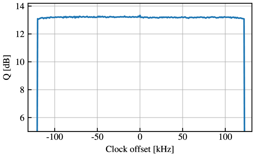
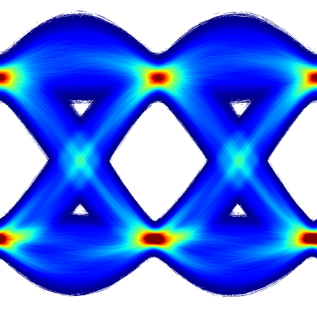
The performance of clock-recovery is evaluated using PAM /̄4 and PAM /̄8 signals in back-to-back transmission. Fig. 6 shows the Q-factor versus the clock-frequency offset between transmitter and receiver clock when transmitting PAM /̄4 signals. An attenuator limited the power into the photodiode to to introduce enough noise and thus bit errors to properly evaluate performance when changing the clock-frequency offset. Performance is stable for a wide range of offsets, showing the resiliance of the implemented algorithms. Performance drops off very rapidly when an offset of () or more is applied, which can be attributed an implementation choice to use an 8-bit integer to keep track of number of symbols added or removed throughout the buffer. A change to a 16- or even 32-bit number would greatly increase clock-frequency offset tolerance, but was deemed unnecessary.
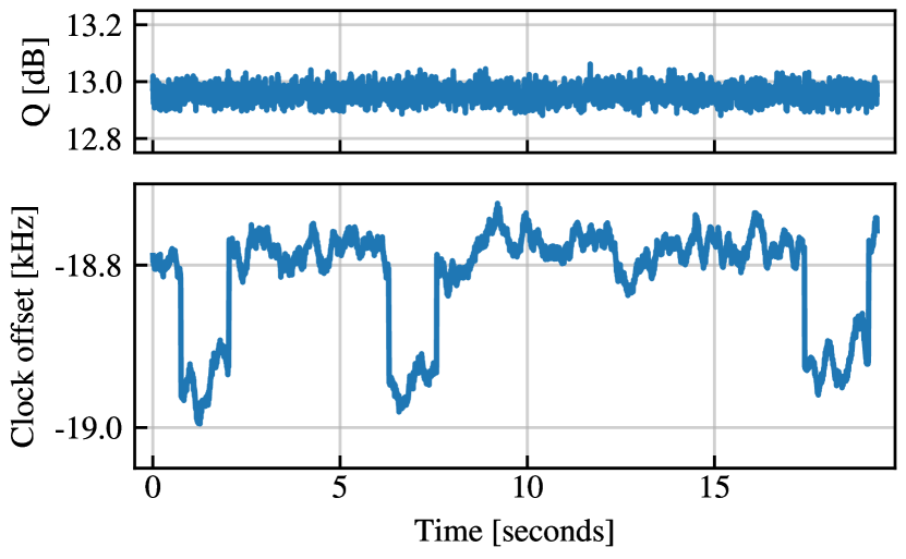
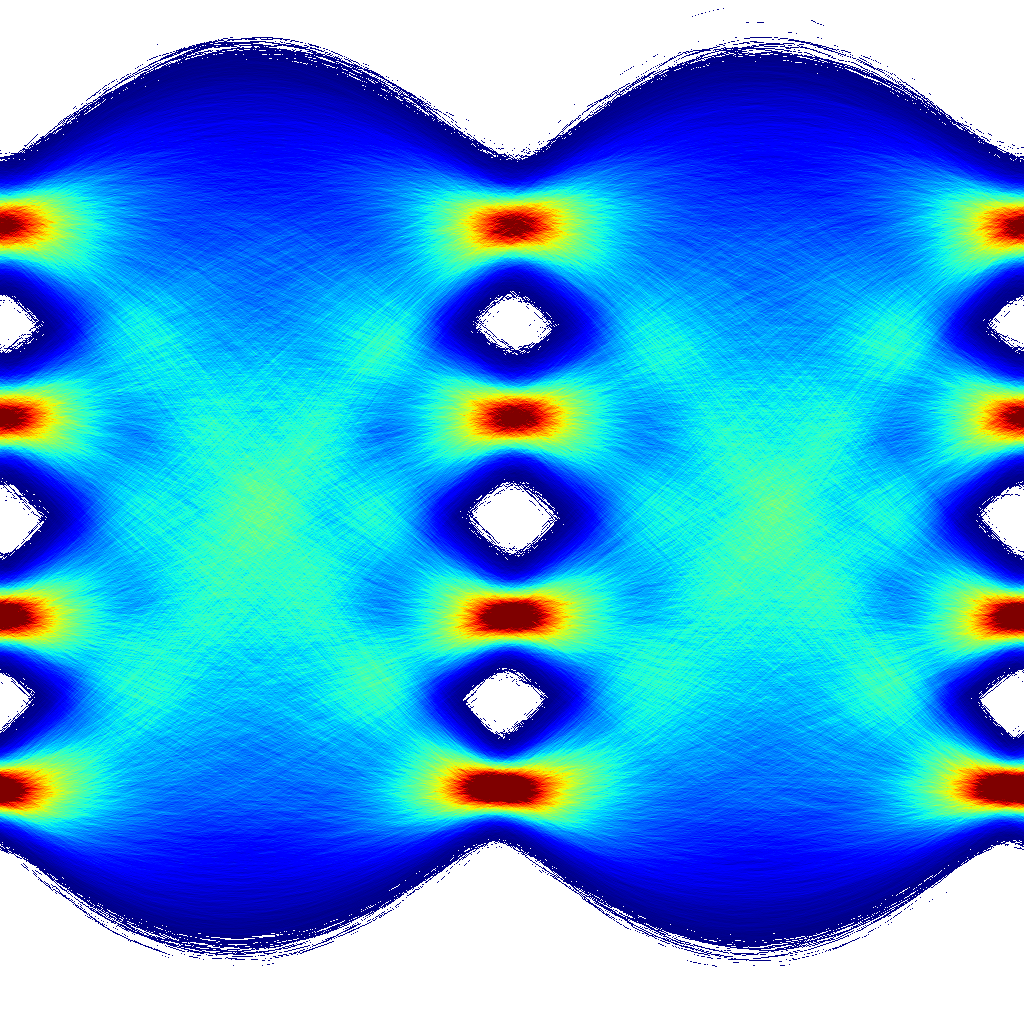
Fig. 7 shows clock-frequency offset and Q-factor over time for PAM /̄8 signals at input power when using free-running clocks. The transmitter digital-to-analog converter (DAC) is driven by a laboratory-grade tone-generator whilst the ADC uses its own internal clock source. Even when the clock-frequency offset experiences rapid changes as shown in Fig. 7, the Q-factor remains constant, demonstrating that the clock-recovery algorithm is able to cope with these rapid transitions. Since the ADC manufacturer advises against the use of the internal clock, the authors consider this a worst-case test. For the remainder of this work, the ADC received a high-quality clock-signal from a laboratory-grade tone-generator.
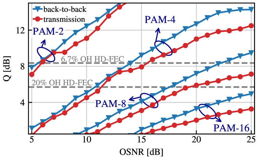
Fig. 8 shows the Q-factor as a function of OSNR for PAM /̄2, PAM /̄4, PAM /̄8, and PAM /̄16. In back-to-back, performance reaches the Q-factor threshold for 6.7% overhead HD-FEC [22] at , , and for PAM /̄2, PAM /̄4, and PAM /̄8, respectively. PAM /̄16 can be decoded in real-time using the GPU DSP, but signal quality is not sufficient to reach the threshold for either 6.7% or 20%[22] overhead HD-FEC. Most likely this is due to severe low-pass filtering of the signal by the receiver components. The signal with 50% RRC roll-off uses of electrical bandwidth, whilst the bandwidth of the photodiode and ADC are both . The static equalizer (see Section III and Fig. 4, step 2) can boost the attenuated higher frequencies, but only at the cost of amplifying noise. Future ADCs (PCIe Gen 4) offer greater bandwidth and sampling rate, facilitating greater baud and data rates. Proprietary interfaces such as NVIDIA NVLink [24] can support a further tenfold increase.
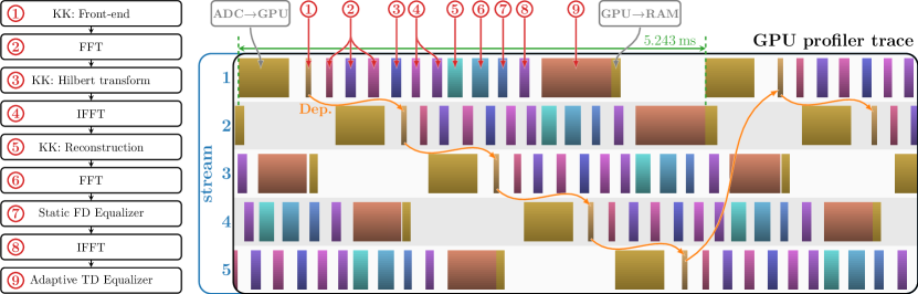
IV KK GPU Implementation and Evaluation
We chose to implement KK field reconstruction to showcase GPU excellence in handling large FFTs and exploiting its enhanced capability for frequency-domain signal processing. Fig. 9 shows the DSP chain for KK N/̄QAM signals subdivided in 9 steps, each of which an algorithm performed by one or more kernels as described in this section. Five parallel streams are used as shown in the profiler trace. Dependencies between streams are marked as Dependency and annotated with orange arrows in the profiler trace.
IV-A Step 1: Overlap and KK Front-end
The KK Front-end containing the square root and logarithm operations are incorporated into the overlap kernel to limit GPU memory access and thus improve performance. The overlap part of this kernel, including the dependency handling via events, see Section II-D and Fig. 2.
Since the digitizer used in this experiment was AC-coupled, no DC-terms are measured, hampering KK field reconstruction. Therefore, an offline-optimized static DC-offset is added to the signal [25] after the data are converted from 12-bit unsigned integers to 32-bit floats. Subsequently, a conventional KK front-end[19] performs the square root, to retrieve the signal amplitude, and logarithm, required for phase reconstruction, operations at 4 samples-per-symbol.
IV-B Step 2-5: Hilbert transform and KK field reconstruction
A 100% overlap-save 1024-point real-to-complex FFT is used to convert the samples pre-processed for phase-retrieval by the KK front-end to frequency domain, dividing the 222 samples in the buffer in 8192 blocks of 1024 samples of which, because of 100% overlap-save, 512 are valid. The Hilbert transform is performed in FD before a complex-to-complex IFFT converts back to TD. Now, the KK field reconstruction[19] combines the previously retrieved signal amplitude with the phase recovered through the logarithm and Hilbert transform. The recovered optical field is downshifted to DC for further processing.
IV-C Step 6-8: FD static equalization
After a 1024-point complex-to-complex FFT, the recovered signal is filtered in FD by a static 203-tap FIR filter, which is optimized offline beforehand and uploaded to GPU memory. This static equalizer compensates for receiver bandwidth impairments and performs matched filtering for the RRC N/̄QAM signals. A 512-point IFFT both converts the signal to TD and downsamples it to 2 samples-per-symbol.
IV-D Step 9: TD adaptive equalization and symbol decision
Clock-phase and symbol-phase recovery, transmitter IQ-imbalance compensation, and symbol decision and demapping are performed by a 4-tap adaptive widely-linear[26] TD decision-directed least mean square (DD-LMS) equalizer. Note that in contrast to the PAM /̄N signals of Section III, a reference clock was shared by transmitter and receiver, so the equalizer only needs to handle relatively small clock-phase and symbol-phase fluctuations, for example due to changing conditions in the field-deployed fiber. During equalization, the decisions made by the equalizer are demapped and stored in GPU memory to be sent to RAM after this kernel is finished.
Four taps was deemed sufficient and has the benefit of exploiting 128-bit parallel data access through vector load/store instructions as explained in Section III-A. Furthermore, warp-level shuffles are used to further optimize this TD adaptive equalizer kernel which is serial in nature. One might conclude based on the GPU profiler trace in Fig. 9 that this kernel uses a lot of resources since it uses a lot of time. However, this is not correct. A relatively low amount of GPU parallel processing units are used for execution of this kernel. Therefore, this kernel does not take up significant amount of resources even though it takes up significant amount of time, similar to the clock-phase unwrapping kernel discussed in Section III-B. The unused parallel processing units can be used by other parallel processing streams, see Fig. 9.
IV-E Back-to-back evaluation of N-QAM signals
KK N/̄QAM signals are generated using the same setup as PAM /̄N signals explained in Sections III-D and 5. However, the IQM is operated at the minimum optical output bias point, whilst the AWG produces baseband 1 GBaud N/̄QAM signals with 1% roll-off RRC pulse shaping combined with a digitally-introduced carrier tone at 0.547 GHz. The tone power can be chosen to produce the desired CSPR. Note that the N/̄QAM required optical bandwidth is half of PAM /̄N, but the required electrical bandwidth is identical.
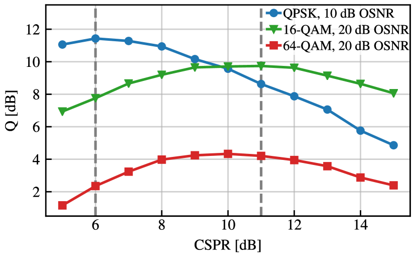
CSPR optimization is important for KK N/̄QAM signals since it directly influences the accuracy of signal reconstruction and OSNR performance. When employing high carrier power, signal-signal beat interference (SSBI) is lower and signal reconstruction through the KK algorithm is better, thus improving signal quality after receiver DSP. However, higher carrier power leads to lower signal power for the same combined power. Therefore, signal quality degrades in the higher CSPR region, as can be seen in Fig. 10. The choice of CSPR is essentially a trade-off between increased reconstruction error at lower CSPRs versus increased noise at higher CSPRs. Moreover, the optimal choice also depends on modulation cardinality, since high-cardinality modulation formats such as 64/̄QAM suffer more from reconstruction errors than 4/̄QAM. For simplicity of measurement, the CSPR is optimized at only one specific value for OSNR, for 4/̄QAM and for 16/̄QAM and 64/̄QAM. A CSPR of is chosen for 4/̄QAM whilst is employed for 16/̄QAM and 64/̄QAM throughout this work.
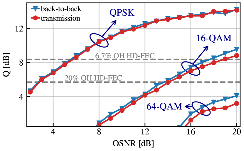
Fig. 11 shows the Q-factor as a function of OSNR for 4, 16, and 64/̄QAM. 4/̄QAM reaches the 6.7% overhead HD-FEC threshold[22] at OSNR, whilst 16/̄QAM requires an OSNR of . 64/̄QAM signals were received and processed in real time, however, performance was not sufficient to reach either the 6.7% of 20% overhead HD-FEC threshold[22].
V Experimental field trial
V-A Experimental setup
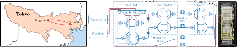
The same transmitter and receiver architecture used for back-to-back characterization, see Figs. 5, III-D and IV-E, is also used to generate and receive the signals in the field trial scenario. The signal launch power is set by an EDFA followed by a VOA. The transmission network shown in Fig. 12 consists of a bidirectional ring with 3 commercial ROADMs. Two ROADMs are installed in the same location in Koganei, Tokyo. The link between these ROADMs is relatively short and its loss was set to using fixed attenuators. Both ROADMs are connected to a commercial ROADM in Otemachi, Tokyo by a , 4-fiber link. The transmission loss, including optical distribution frames, is . 56% of the fiber is installed in underground ducts and the remainder on areal paths and in the surface along railway tracks. The red line in Fig. 12) shows the signal path along the network, with a total transmission distance of . Each ROADM has two line sides, each consisting of wavelength selective switchs (WSSs) and optical amplifiers for add/drop and express connections. In addition, arrayed-waveguide gratings (ArrWGs) were used for add and drop. Fig. 12 shows a photograph of one of the commercial ROADMs.
V-B Transmission results of PAM /̄N signals
Fig. 8 shows the Q-factor as a function of OSNR for PAM /̄2, PAM /̄4, PAM /̄8, and PAM /̄16 for back-to-back and after transmission through the field trial network. An OSNR penalty increasing with modulation cardinality, is observed. The penalty at the 6.7% overhead HD-FEC threshold is and for PAM /̄2 and PAM /̄4, respectively. After transmission through the field trial network, PAM /̄8 cannot be recovered using a 6.7% overhead HD-FEC, but can when a 20% overhead HD-FEC with a Q-factor threshold of is employed[22]. Eye diagrams for PAM /̄N transmission over the field trial network without noise loading are plotted in Fig. 13.
V-C Transmission results of N-QAM signals
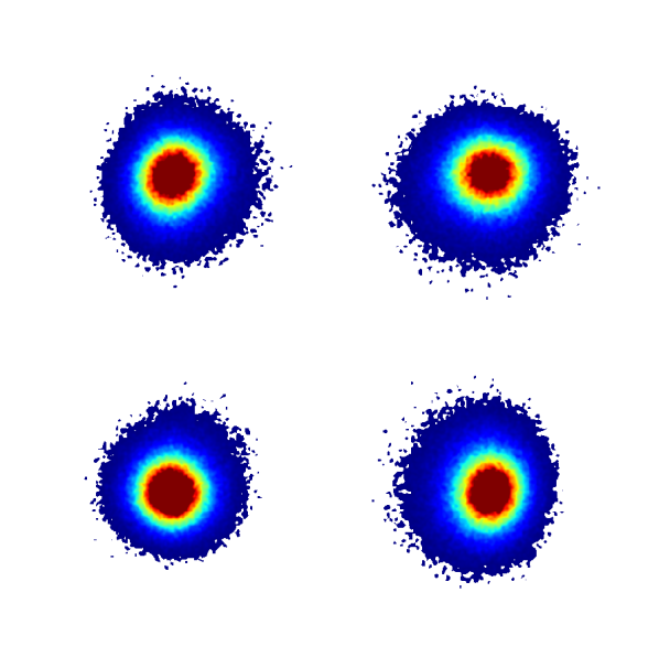
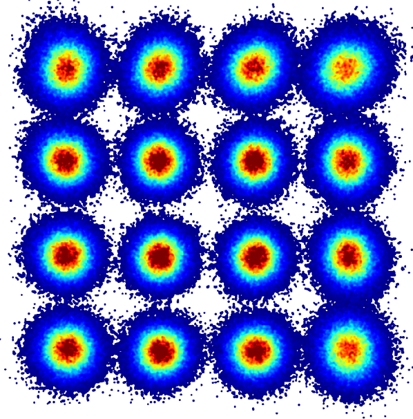
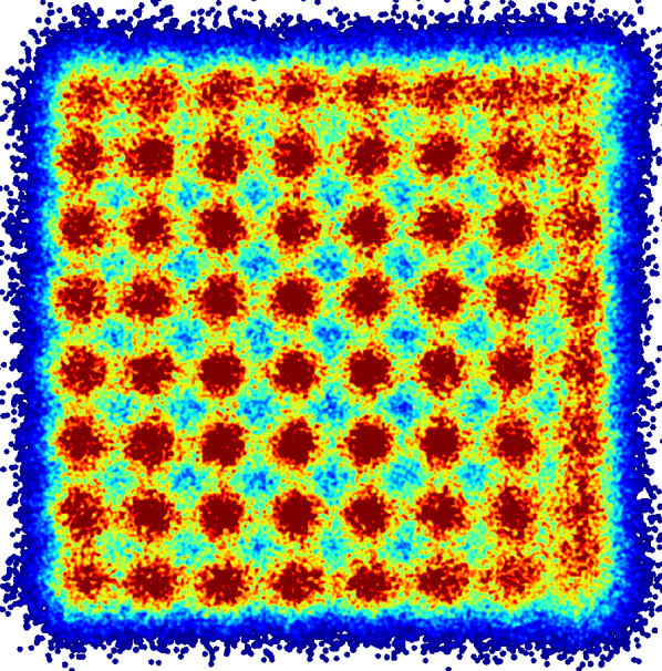
Fig. 11 shows the Q-factor as a function of OSNR for 4/̄QAM, 16/̄QAM, 64/̄QAM for back-to-back and after transmission through the field trial network. A and OSNR penalty is observed for 4/̄QAM and respectively. 64/̄QAM signals were received and processed in real time, however, performance was not sufficient to reach either the 6.7% of 20% overhead HD-FEC threshold[22]. Constellation diagrams for these modulation formats at maximum available OSNR after transmission over the field trial network are plotted in Fig. 14.
V-D Continuous real-time transmission
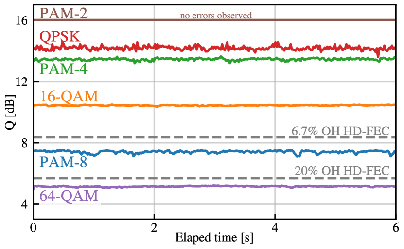
Fig. 15 shows the short-term average Q-factor for six second long traces for various modulation formats. Within these six seconds, all transmitted symbols were received, processed, and recorded continuously, using the real-time GPU algorithms detailed in the previous sections. During these six seconds, 6 billion symbols were received for N/̄QAM signals and 12 billion symbols for PAM /̄N signals. The Q-factor displayed in Fig. 15 is estimated from the bit error rate (BER) in sections of . For all transmitted signals, we observe stable performance. No errors are observed while transmitting PAM /̄2. 4/̄QAM, PAM /̄4, and 16/̄QAM can be recovered using a 6.7% overhead HD-FEC since the Q-factors are , , and , respectively. With a Q-factor of , PAM /̄8 cannot be recovered by the 6.7% overhead HD-FEC but performance is sufficient for 20% overhead error coding. 64/̄QAM is successfully transmitted, received, processed using the GPU, and stored in RAM in real time, but performance is not sufficient for HD-FEC algorithms considered.
VI Conclusion
A real-time, software-defined, multi-modulation-format, GPU-based receiver achitecture is introduced, detailed, and demonstrated to achieve stable real-time operation over a field-deployed metropolitan network. We show the potential for massive parallel processing provided by a GPU to recover directly-detected PAM /̄N signals as well as N/̄QAM signals with Kramers-Kronig coherent detection. optical signals using PAM /̄2, PAM /̄4, PAM /̄8, and PAM /̄16 modulation, 4/̄QAM, 16/̄QAM, and 64/̄QAM modulation, are received and processed in real time by our flexible receiver architecture. PAM /̄2 and -4 and 4- and 16/̄QAM reach the Q-factor threshold for a 6.7% overhead HD-FEC both in back-to-back and after transmission through the field-trial network. PAM /̄8 reaches this threshold in back-to-back, but no longer after transmission, although it can be received using a 20% overhead HD-FEC. PAM /̄16 and 64/̄QAM are received and processed in real-time, but performance is not sufficient to reach either HD-FEC threshold. Continuous real-time transmission reveals stable performance despite the varying environment of installed fiber. These results show the potential of massive parallel processing provided by GPUs for low-cost flexible optical links for a range of modulation formats.
References
- [1] OIF “OIF-400ZR Implementation Agreement” URL: https://www.oiforum.com/technical-work/implementation-agreements-ias/
- [2] G. Kakkavas “A Software Defined Radio Cross-layer Resource Allocation Approach for Cognitive Radio Networks: From Theory to Practice” In IEEE Transactions on Cognitive Communications and Networking, 2020, pp. 1–1 DOI: 10.1109/TCCN.2019.2963869
- [3] “GNU Radio” Accessed: 2020-11-23, https://www.gnuradio.org
- [4] Tarik Kazaz “Hardware Accelerated SDR Platform for Adaptive Air Interfaces”, 2017 arXiv:1705.00115 [cs.NI]
- [5] S. Randel et al. “First real-time coherent MIMO-DSP for six coupled mode transmission” In 2015 IEEE Photonics Conference (IPC), 2015 DOI: 10.1109/IPCon.2015.7323761
- [6] S. Beppu et al. “Real-time strongly-coupled 4-core fiber transmission” In Optical Fiber Communication Conference (OFC) 2020 Optical Society of America, 2020, pp. Th3H.2 DOI: 10.1364/OFC.2020.Th3H.2
- [7] Shohei Beppu et al. “Weakly coupled 10-mode-division multiplexed transmission over 48-km few-mode fibers with real-time coherent MIMO receivers” In Opt. Express 28.13 OSA, 2020, pp. 19655–19668 DOI: 10.1364/OE.395415
- [8] P.. Winzer and D.. Neilson “From Scaling Disparities to Integrated Parallelism: A Decathlon for a Decade” In J. of Lightw. Technol. 35.5, 2017, pp. 1099–1115
- [9] Yifan Sun “Summarizing CPU and GPU Design Trends with Product Data” arXiv: 1911.11313 In arXiv:1911.11313 [cs], 2019
- [10] Murad Qasaimeh “Comparing Energy Efficiency of CPU, GPU and FPGA Implementations for Vision Kernels” In 2019 IEEE International Conference on Embedded Software and Systems (ICESS), 2019, pp. 1–8
- [11] R. Li et al. “A multi-standard efficient column-layered LDPC decoder for Software Defined Radio on GPUs” In 2013 IEEE 14th Workshop on Signal Processing Advances in Wireless Communications (SPAWC), 2013, pp. 724–728 DOI: 10.1109/SPAWC.2013.6612145
- [12] T. Suzuki et al. “Demonstration of 10-Gbps Real-Time Reed–Solomon Decoding Using GPU Direct Transfer and Kernel Scheduling for Flexible Access Systems” In Journal of Lightwave Technology 36.10, 2018, pp. 1875–1881 DOI: 10.1109/JLT.2018.2793938
- [13] T. Suzuki et al. “10-Gb/s Software Implementation of Burst-Frame Synchronization Using Array-Access Bitshift and Dual-Stage Detection for Flexible Access Systems” In Journal of Lightwave Technology 36.23, 2018, pp. 5656–5662 DOI: 10.1109/JLT.2018.2870912
- [14] Takahiro Suzuki “Software Implementation of 10G-EPON Upstream Physical-Layer Processing for Flexible Access Systems” In J. of Lightw. Technol. 37.6, 2019, pp. 1631–1637
- [15] T. Suzuki, S. Kim, J. Kani and J. Terada “Demonstration of Fully Softwarized 10G-EPON PHY Processing on a General-Purpose Server for Flexible Access Systems” In Journal of Lightwave Technology 38.4, 2020, pp. 777–783 DOI: 10.1109/JLT.2019.2948333
- [16] S. Kim et al. “Coherent Receiver DSP Implemented on a General-Purpose Server for Full Software-Defined Optical Access” In 2018 Optical Fiber Communications Conference and Exposition (OFC), 2018, pp. 1–3
- [17] S. Kim, T. Suzuki, J. Kani and A. Otaka “Coherent receiver DSP implemented on a general-purpose server for a full software-defined access system” In IEEE/OSA Journal of Optical Communications and Networking 11.1, 2019, pp. A96–A102
- [18] T. Suzuki “Real-Time Implementation of Coherent Receiver DSP Adopting Stream Split Assignment on GPU for Flexible Optical Access Systems” In J. of Lightw. Technol. 38.3, 2020, pp. 668–675
- [19] Antonio Mecozzi, Cristian Antonelli and Mark Shtaif “Kramers Kronig coherent receiver” In Optica 3.11, 2016, pp. 1220 DOI: 10.1364/OPTICA.3.001220
- [20] “Japan Gigabit Network (JGN)” Accessed: 2020-11-23, https://testbed.nict.go.jp/jgn/
- [21] Sjoerd Heide et al. “Real-time, Software-Defined, GPU-Based Receiver Field Trial” In arXiv preprint arXiv:2010.14333, 2020
- [22] Erik Agrell and Marco Secondini “Information-Theoretic Tools for Optical Communications Engineers” In 2018 IEEE Photonics Conference (IPC) IEEE, 2018, pp. 1–5 DOI: 10.1109/IPCon.2018.8527126
- [23] Kuang-Tsan Wu and Han Sun “Frequency-Domain Clock Phase Detector for Nyquist WDM Systems” In Optical Fiber Communication Conference Optical Society of America, 2014, pp. Th3E.2 DOI: 10.1364/OFC.2014.Th3E.2
- [24] NVIDIA “NVIDIA A100 Tensor Core GPU Architecture” pp. 52-53, Accessed: 2020-12-28 URL: https://www.nvidia.com/content/dam/en-zz/Solutions/Data-Center/nvidia-ampere-architecture-whitepaper.pdf
- [25] Ruben S. Luís et al. “Simple method for optimizing the DC bias of Kramers-Kronig receivers based on AC-coupled photodetectors” In Opt. Express 28.3 OSA, 2020, pp. 4067–4075 DOI: 10.1364/OE.383369
- [26] E.. da Silva and D. Zibar “Widely Linear Equalization for IQ Imbalance and Skew Compensation in Optical Coherent Receivers” In Journal of Lightwave Technology 34.15, 2016, pp. 3577–3586
| Sjoerd van der Heide (S’13) was born in ’s-Hertogenbosch, the Netherlands, in 1992. He received the B.Sc. and M.Sc. (cum laude) degrees in Electrical Engineering from Eindhoven University of Technology, the Netherlands, in 2015 and 2017, respectively. He is currently working towards a PhD degree at the High Capacity Optical Transmission Laboratory, Electro-Optical Communications group, at Eindhoven University of Technology. His research interests include space-division multiplexing and digital signal processing. He is the recipient of a student paper award at ECOC 2018 and a best paper award at OECC 2019. |
| Ben Puttnam (M’12) is a senior researcher in the Photonic Network System Laboratory at the National Institute of Information and Communications Technology (NICT) in Tokyo, Japan. He received the MPhys degree in Physics from the University of Manchester (UK) in 2000 and the PhD degree from University College London in 2008, working as a Switch Design Engineer for T-mobile (UK) in between. After short term visits to NICT, supported by JSPS and the Photonics group at Chalmers University, Göteborg, Sweden supported by the Ericsson research foundation he re-joined NICT in March 2010. His research interests are space-division multiplexing for optical transmission and optical signal processing. |
| Georg Rademacher (M’14, SM’20) received the Dipl.-Ing. and Dr.-Ing. degree in electrical engineering from Technische Universität Berlin, Germany, in 2011 and 2015, respectively. During his doctoral studies, he did internships at Bell Laboratories in Holmdel, USA and the National Institute of Information and Communications Technology (NICT) in Japan. In 2016 he joined the Photonic Network System Laboratory at NICT in Tokyo, Japan, where he is engaged in research on subsystems and systems for efficient high capacity optical transmission. |
| Chigo Okonkwo (M’09–SM’18) was born in Wakefield, U.K., in 1979. He received the Ph.D. degree in optical signal processing from the University of Essex, Colchester, U.K., in 2010. Between 2003 and 2009, he was a Senior Researcher with the Photonic Networks Research Lab, University of Essex, U.K. After his Ph.D., he was appointed as a Senior Researcher with the Electro-optical communications group working on digital signal processing techniques and the development of space division multiplexed transmission (SDM) systems. He is currently an Associate Professor and leads the High-capacity optical transmission laboratory within the Institute for Photonic Integration (former COBRA), Department of Electrical Engineering, Eindhoven University of Technology (TU/e), The Netherlands. He was instrumental to the delivery of the first major SDM project in the European Union—MODEGAP project. Since 2014, he has been tenured at the ECO group, where he has since built up a world-class laboratory collaborating with several industrial and academic partners. His general research interests are in the areas of optical and digital signal processing, space division multiplexing techniques, and long-haul transmission techniques. In 2018, he was TPC chair for subcommittee 3 on digital signal handling. Between 2015 and 2017, he served on the TPC for the OSA conference on signal processing in photonic communications (SPPCom). In 2017 and 2018, he was the Program Chair and the Conference Chair at SPPCom, respectively. Dr. Okonkwo recently served as an associate editor for special edition of the IEEE Journal on Lightwave Technology. For the next 3 years, he has been retained to serve as technical programme subcommittee on Fiber-optic and waveguide devices and sensors (subcommittee D5) at Optical fiber communications conference OFC 2020-2022. |
| Satoshi Shinada (Member, IEEE) received the B.S. degree from Science University of Tokyo in 1998 and the M.E. and Ph.D. degrees from Tokyo Institute of Technology in 2000 and 2002, respectively. In 2002 he joined the Precision and Intelligence Laboratory, Tokyo Institute of Technology as a JSPS Post-Doctoral Fellow. Since 2003, he has been with National Institute of Information and Communications Technology (NICT), Tokyo Japan. From 2015 to 2016, he was a Deputy Director of the Ministry of Internal Affairs and Communications, Japan. He has been engaged in the research and development on LiNbO3 optical modulators, optical switches, optical interfaces for single flux quantum circuit and optical packet switching (OPS) systems. Dr. Shinada received the IEEE/LEOS Student Award in 2002, and the 2015 Ichimura Prize in Science for Excellent Achievement from the New Technology Development Foundation. He is a member of IEEE, IEEE Photonics Society, the Japan Society of Applied Physics (JSAP) and the Institute of Electronics, Information and Communication Engineers of Japan (IEICE). |