Geometrical Characterization of Glass Nanopipettes with Sub-10 nm Pore Diameter by Transmission Electron Microscopy
Abstract
Glass nanopipettes are widely used for various applications in nanosciences. In most of the applications, it is important to characterize their geometrical parameters, such as the aperture size and the inner cone angle at the tip region. For nanopipettes with sub-10 nm aperture and thin wall thickness, transmission electron microscopy (TEM) must be most instrumental in their precise geometrical measurement. However, this measurement has remained a challenge because heat generated by electron beam irradiation would largely deform sub-10-nm nanopipettes. Here we provide methods for preparing TEM specimens that do not cause deformation of such tiny nanopipettes.
INTRODUCTION
Glass nanopipettes have numerous applications in nanosciences, such as single molecule sensing of macromolecules and their interactions Yu et al. (2017) and local delivery of molecules Ivanov et al. (2015). In many applications (if not all), the nanopipette geometrical parameters, such as the inner and outer cone angles, pore and central channel diameters, and wall thickness are important determinants of the application performance Sze et al. (2015), as typically seen in scanning ion conductance microscopy (SICM) Hansma et al. (1989); Novak et al. (2009); Klausen et al. (2016); Watanabe and Ando (2017). The spatial resolution of SICM is strongly dependent on the nanopipette tip geometry Rheinlaender and Schäffer (2015, 2009); Weber and Baker (2014); Edwards et al. (2009); Rheinlaender and Schäffer (2017); Del Linz et al. (2014). The assessment of detailed tip geometry is thus important for the optimization of nanopipette-based measurements. Two methods and their combination have been widely used for this assessment: electrical measurements of the ion current resistance and scanning electron microscopy (SEM) imaging Rheinlaender and Schäffer (2017). The ion current resistance is related to the pore diameter and the inner half cone (IHC) angle Tognoni et al. (2016); Perry et al. (2016a); Ying et al. (2002). The IHC angle cannot be directly assessed in both measurements. Therefore, it is usually estimated from the outer cone angle given by SEM images of the nanopipette by assuming a constant ratio of outer to inner radius, or from the pore size given by SEM images and the ion current resistance Rheinlaender and Schäffer (2017). When nanopipette fabrication can be performed with good reproducibility of a constant geometry, the pore diameter can be estimated from the electrical measurement alone using the IHC angle pre-estimated from SEM measurements for a few nanopipettes. However, SEM visualizes the pipette outer shape and pore after pretreatment with metal-coating, and therefore, the measured geometrical parameters are affected by the metal-coating.
Direct observation of the detailed tip geometry of nanopipettes has been achieved using transmission electron microscopy (TEM) Chen et al. (2017); Sa and Baker (2013a); Perry et al. (2016a). From their TEM images, the pore diameter, IHC angle, and the internal channel can be directly and accurately measured. However, it is still challenging to perform TEM measurements for pipettes with pore diameter less than Perry et al. (2016a), particularly to get their consistent images. In TEM measurements of smaller nanopipettes with thin wall, deformation of their tip caused by the electron beam-generating heat is a serious problem Chen et al. (2017). The optimization of TEM measurements is therefore important in overcoming this heating problem and thereby achieving precise characterization of the geometry, particularly for nanopipettes with sub-10 nm diameter (referred to as sub-10-nm nanopipettes hereafter).
In this report, we describe methods to fabricate sub-10 nm nanopipettes with good reproducibility and to characterize their tip geometry with TEM without causing tip deformation. In addition, we provide an easy method to prepare a large number of tip segments on a TEM grid. These methods facilitate tuning and optimization of sub-10 nm nanopipette fabrication for practical applications.
MATERIALS AND METHODS
Materials.
KCl and FeCl3 solutions were prepared using deionized (DI) Milli-Q water (resistivity, at ). The FeCl3 solution was used to prepare Ag/AgCl electrodes Polk et al. (2006). KCl and FeCl3 were purchased from Funakoshi Co. (Tokyo, Japan) and Sigma-Aldrich (MS, USA), respectively. A flexible syringe needle made of plastic and fused silica (World Precision Instruments, Microfil, MF34G-5) was used to fill nanopipettes with DI water or KCl solution.
Sub-10 nm Nanopipette Fabrication.
All sub-10 nm nanopipettes used in this study were fabricated from quartz capillaries with an inner diameter of and an outer diameter of (Q100-30-1.5, Sutter Instrument, CA, USA). The capillaries were cut into length with a custom-made pipe cutter. Nanopipettes were then fabricated with a laser puller (P-2000, Sutter Instrument, CA, USA). The details of pulling parameters used for the laser puller are provided in Supporting Information, Table S1.
Current-Voltage Curve Analysis.
The current-voltage () relationship was measured using the method previously described Sun et al. (2019) to estimate the nanopipette pore diameter before TEM measurements. The nanopipettes were first filled with DI water by a thermally driven method Sun et al. (2019). Then, a large fraction (98%) of water inside the pipette was replaced with KCl solution by injecting it. The nanopipettes were incubated for . For assurance of full solution exchange, the nanopipettes were subsequently immersed in a bath solution of KCl for . The absence of a concentration gradient in the tip was confirmed by an measurement over time (Supporting Information, SI 8).
Before the measurement, the tip of the pipette was washed with DI water to remove any contamination. Ag/AgCl electrodes were prepared by dipping Ag wires into FeCl3 solution for one min Polk et al. (2006). The ion current was amplified with an amplifier (Axopatch 200B, Molecular Devices, LLC, CA, USA). A Faraday cage was used to suppress electrical noise in the measurements. A narrow range of bias voltage (between to ) was used, in which ion current rectification was negligible (Figure. S6). The pipette resistance (VI) was analyzed as a function of measured pore diameter, IHC angle, and ion conductivity ( at for KCl) using a lab-made program based on MATLAB (MathWorks, Inc., MA, USA).
Sample Rreparation for TEM Observations.
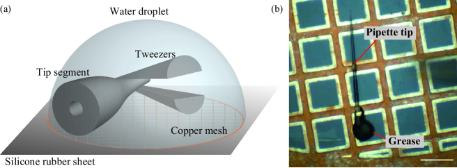
After the measurements, the KCl solution in the nanopipettes was exchanged to DI water. These pipettes were then stored overnight in DI water to remove residual ions. To have a short segment containing the intact tip portion of a nanopipette, the nanopipette was cut in a deionized water droplet on a TEM grid, using a micromanipulator and a micro-tweezers (AxisProSS, Micro Support, Shizuoka, Japan) (Supporting Information, Movie 1). The water droplet functions as (i) a cushion against damage of the tip end that would otherwise occur when a cut segment is deposited on the TEM grid, and as (ii) a cage that traps the cut segment in the water droplet. The TEM grid was placed on a hydrophobic silicone rubber sheet (Figure 1a), which facilitated the formation of a hemisphere-shaped water droplet on the TEM grid. After cutting a number of nanopipettes in this way, we confirmed that all the resulting segments were on the TEM grid. After full evaporation of the water droplet, the tip segments were properly positioned on the TEM grid, using the micromanipulator with a probe (Supporting Information, Movie 2). TEM copper grids with or without a formvarcarbon membrane were used to investigate how the membrane affects the heat-induced tip deformation during TEM measurements.
TEM Measurements.
The TEM grid on which the nanopipette segments had been properly positioned was placed in the chamber of the TEM apparatus (JEOL 2100 plus). TEM measurements were performed at acceleration voltage. The minimum dose system (MDS), a measurement mode in the TEM apparatus, was used to minimize tip deformation. In the MDS, the electron beam irradiates the sample only when the TEM image is captured. The beam irradiation time for capturing an image was set at one second. By utilizing the MDS, we were able to precisely control the total amount of electron dose during imaging, which allowed us to examine an effect of heat generated by electron-beam irradiation. All TEM images were captured at a magnification range between 40,000 and 80,000. The electron dose during image acquisition was estimated from the current density.
RESULTS AND DISCUSSION
Fabrication of Nanopipettes.
Sub-10 nm nanopipettes were fabricated using the laser puller P-2000, in which a long glass capillary was clamped at their ends. The parameters for the puller action listed in Supporting Information, Table S1, were used. We noticed that the precise control of heat dissipation during the pulling process was important for producing sub-10 nm pipettes with high reproducibility. The rate and amount of heat dissipation are sensitive not only to the area and position at which the glass capillary is clamped but also to the clamping force. The silicone rubber used to clamp a glass capillary deforms depending on the magnitude of clamping force. Therefore, the shape of a produced nanopipette is affected by the clamping force. To control the clamping force precisely, we used a torque driver and a custom screw head. Details are provided in Supporting Information, Section SI 2.
Alignment of Nanopipette Segments on TEM Grid.
Figure 1 shows how a short tip segment was prepared on a copper mesh TEM grid. Using a micro tweezers, a nanopipette whose back side was held was cut in a water droplet on the TEM grid supported on a silicone rubber sheet (Figure 1a). The water droplet prevented the resulting tip segment from escaping from the TEM grid and also from damage, allowing us to efficiently prepare a large number of segments on a TEM grid (Supporting Information, Movie 1). After the water droplet evaporated, the segments remained on the grid but their position and orientation unavoidably changed; their tip portions were often superposed on the copper mesh. We used the micromanipulator with a glass probe to move each segment so that its tip end portion was not superposed on the copper mesh. Before the positional adjustment of a segment, it was necessary to put a small amount of silicone grease on the back end of the segment. The segment would otherwise be knocked off the TEM grid because of electrostatic interactions between the segment and the glass probe. Figure 1b shows a magnified image of a tip segment on a TEM grid after its positional adjustment. The entire process of this positional adjustment is provided in Supporting Information, Movie 2 and Section SI 3.
Importance of Membrane on TEM Grid.
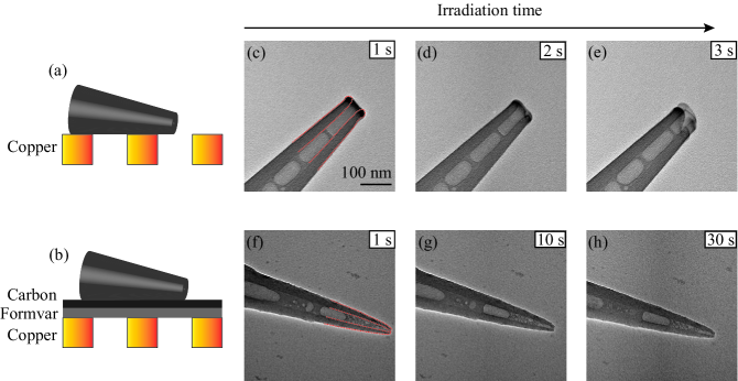
Here we describe the importance of the use of a formvarcarbon-coated grid in TEM measurements of the sub-10 nm nanopipette tip. The tip portion of a sub-10 nm nanopipette segment must be more susceptible to electron beam-generating heat, compared to a tip with a larger pore and a thicker wall. In TEM measurements, the use of a membrane-coated TEM grid is known quantitatively to suppress heat damage of specimens. However, the effectiveness of the suppression largely depends on the specimen used. We investigated how the tip segment of a sub-10-nm nanopipette would deform during its TEM measurements using TEM grids with and without a formvarcarbon membrane.
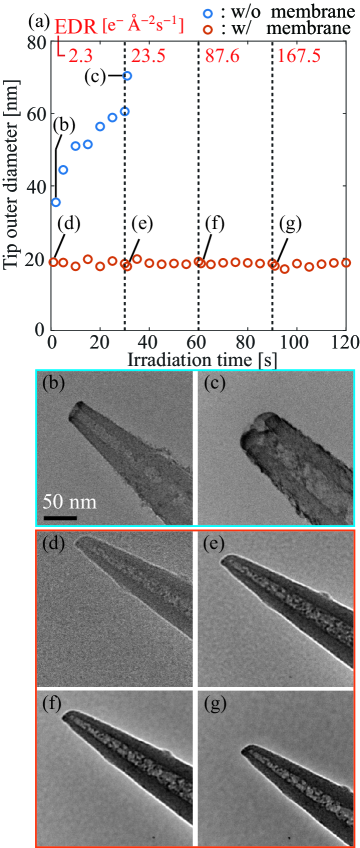
Figure 2 shows time-lapse TEM images of tip segments placed on TEM grids with and without the membrane. These segments were obtained from two nanopipettes fabricated under an identical condition. These TEM images were captured at with an electron dose rate (EDR) of . The TEM images taken without the membrane (Figure 2c–e) show noticeable deformation at the tip region even at = . This deformation becomes significant at = 2 and . In contrast, the TEM images taken with the membrane (Figure 2f–h) show no discernible deformation even at = . Note that the pore diameter of nanopipettes subjected to the TEM observations are expected to be within (SD, , as described later) before the TEM measurements. We had confirmed this original identical size by measuring ion conductance of these two nanopipettes before their TEM observations. Therefore, the tip shape had already been deformed into a trumpet-like shape at = , when the membrane-less TEM grid was used. In fact, when a membrane-less TEM grid was used, we always observed the trumpet-like shape, even under electron irradiation with a lower EDR of (Supporting Information, Section SI 4, Figure S3). In contrast, when a membrane-coated TEM grid was used, a semi-conical tip shape was always observed.
We further evaluated the heat-induced deformation and the membrane effect against this deformation by varying the irradiation electron density in the TEM measurements (Figure 3). In this evaluation, the outer diameter of the tip end was measured as a function of ED. The EDR was changed in a stepwise manner from 2.3 to . When a membrane-less TEM grid was used, the tip outer diameter increased even under the condition of EDR = , from (Figure 3b) to during the period from = (the first two blue circles in Figure 3b). This large increase was followed by a gradual increase up to at = (the next five blue circles in Figure 3a). When the EDR was increased from 2.3 to , the tip outer diameter suddenly increased from at = (Figure 3c). In contrast, when a membrane-coated TEM grid was used, there was no discernible deformation of the tip even at EDR = , the maximum EDR value for our TEM system (Figure 3d–g). The tip outer diameter remained throughout the observations (red circles in Figure 3a; 18.65 (SD), (SD), 18.61 SD)nm, and (SD) for 2.3, 23.5, 87.6, and , from left to right), indicating effective dissipation of electron beam-generating heat through the membrane. We confirmed this absence of deformation for 26 sub-10 nm nanopipette tips (not shown). In Supporting Information, Table S2, we provided statistics for tip geometry of eight nanopipettes fabricated using the same pulling parameters, as shown in Supporting Information, Table S1. The tip outer diameter assessed using membrane-coated TEM grids ranges between 14.43 and (mean value, ), as shown in Supporting Information, Table S2. These values are much smaller than the value, , observed at = using a membrane-less TEM grid (Figure 3b), suggesting that the heat-induced deformation is significant even with 1–2 s exposure to electron beam (dilation rate, at EDR = ). Thus, the use of membrane-coated TEM grids is essential for the accurate TEM assessment of tip geometry for sub-10 nm nanopipettes.
Geometrical Characterization of sub-10 nm Nanopipettes: TEM Measurements.
Finally, we discuss how the tip geometry of sub-10-nm nanopipettes is related to the pipette resistance . The value obtained by electrical measurements is related to the pore diameter and IHC angle of the nanopipette, and the solution conductivity through the equation
| (1) |
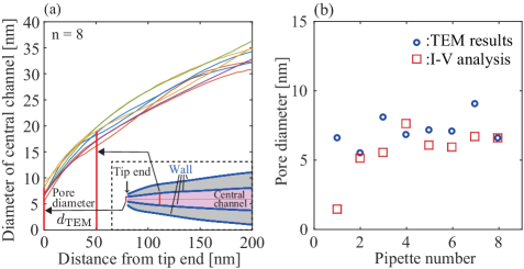
This model Del Linz et al. (2014) assumes a simple conical shape for the tip (i.e., a constant ). However, the tip regions of sub-10-nm nanopipettes directly captured by TEM revealed deviations from a simple conical shape. Figure 4a depicts the diameter of the inner channel as a function of the distance measured from the tip end (tip distance), extracted from TEM images of eight tip segments with (see Supporting Information, sections SI 6 and SI 7). In all cases the diameter does not increase linearly with the tip distance, that is, the IHC angle does not have a single value around the tip, as reported for nanopipettes with larger pore diameters Tognoni et al. (2016). To check how largely the TEM-assessed geometry of a nanopipette tip affects Equation (1), we used a linearly fitted inner half cone (LF-IHC) angle, defined as the slope obtained by linear fitting of each curve, as shown in Figure 4a for the tip distance from 0 to (i.e., approximated IHC angle). For the eight nanopipettes, we compared the values of measured from their TEM images () with those estimated using Equation (1), where was approximated by the LF-IHC angles (Supporting Information, Table S2). The results are shown in Figure 4b. The two sets of measured values of and , distributed around , and their difference were within (SD, ); therefore, a relation of holds (95% confidence interval, for ), where and are the population mean of and , respectively.
Although the LF-IHC angle gives a good estimate of , knowing the variation in the IHC angle in the tip region is still important for the numerical analysis of nanofluidic behavior in nanopipettes, since this analysis requires details of the tip geometry. Finite element analysis simulations on the basis of the coupled Poisson, Nernst–Planck, and Naiver–Stokes equations have been widely used for the analysis of nanopipettes. This yields spatial profiles of physical quantities (such as potential, ion concentration, flow velocity and pressure) around the nanopipette tip. Such spatial information is difficult to obtain experimentally. Nanofluidic behaviors can be analyzed experimentally for nonlinear relationships, which are generally found in nanofluidic systems with broken symmetry, such as nanopores Siwy (2006); Siwy and Fuliński (2004); Cheng and Guo (2007); Yusko et al. (2010); Cao et al. (2011); Qiu et al. (2018); Siwy and Fuliński (2002); Woermann (2003); Cervera et al. (2005); White and Bund (2008); Lan et al. (2016) and nanopipettes Wei et al. (1997); Sa and Baker (2011); Deng et al. (2014). The combined analysis makes it possible not only to improve the quantitative interpretation of experimental data obtained with nanopipettes but also to extend application of nanopipettes. The TEM method will make significant contributions to improving, for example, nano-scale surface charge density (SCD) mapping with SICM Klausen et al. (2016); Fuhs et al. (2018); Perry et al. (2016b, 2015); Page et al. (2016); McKelvey et al. (2014). The importance of accurate characterization of the tip geometry for SCD measurement was pointed out in previous TEM study Perry et al. (2016a). In this application, knowing accurate tip geometries is necessary to quantify the SCD map of the sample because the quantification is sensitive to tip geometries. In fact, quantitative SCD measurements with sub-10 nm spatial resolution is still a challenge Klausen et al. (2016) because of the difficulty of characterizing the geometrical parameters of sub-10 nm nanopipettes. Besides, our TEM method can provide an opportunity to perform SICM measurements in complicated situations. A recent study Rabinowitz et al. (2019) revealed a significant contribution of electroosmotic flow and the SCD of the tip to the measured ion current when a large ion concentration gradient exists around a small aperture of the tip. To quantitatively analyze these contributions to the measured SICM data obtained under such conditions Watanabe et al. (2019), information of the detailed tip geometry is indispensable.
The trumpet-like shaped nanopipettes have been frequently observed in electron microscopy measurements Perry et al. (2016a); Zweifel et al. (2016); Chen et al. (2017); Rabinowitz et al. (2019); Holub et al. (2020); Sa and Baker (2013b); Hao and Zhang (2016); Yuill et al. (2013); Zhu et al. (2020). However, in this study, we were unable to find appropriate pulling conditions that could produce trumpet-liked shaped nanopipettes. This suggests that the trumpet-like shaped nanopipettes are resultant from tip deformation by the electron beam (see Supporting Information, Figures S3 and S5), at least, in TEM measurements of sub-10 nm nanopipettes.
CONCLUSIONS
We have provided the conditions for fabricating sub-10 nm nanopipettes with good reproducibility and procedures for their geometrical characterization by TEM. The TEM imaging following our methods enables quick assessment of tip geometry for many nanopipettes, without deformation of the tip by electron beam-generating heat. Our methods will assist and facilitate the production of smaller nanopipettes and thereby contribute to improving various nanopipette applications.
ASSOCIATED CONTENT
Supporting Information
The Supporting Information is available free of charge at https://pubs.acs.org/doi/10.1021/acs.analchem.0c02884.
Pulling parameters (SI 1 and Table S1), optimized pulling conditions (SI 2 and Figure S1), photograph of tip segments of sub-10-nm nanopipettes on TEM grid (SI 3, Figure S2), trumpet-like shaped nanopipettes observed under different conditions (SI 4, and Figure S3), dynamics of nanobubbles in sub-10 nm nanopipettes (SI 5 and Figure S4), TEM images of sub-10 nm nanopipettes taken using the membrane-coated TEM grid (SI 6 and Figure S5), geometrical parameters obtained from the TEM images (Table S2), traces of the nanopipettes before characterization by TEM imaging (Figure S6), and procedures for extracting geometrical profiles of nanopipettes (SI 7 and Figure S7), and finite element method simulations and experiments for the estimation of relaxation rate of ion concentration gradient in the tip (SI 8 and Figure S8, Figure S9, and Figure S10) (PDF).
Video files are also provided for procedure of cutting nanopipette (Movie 1).
Procedure for position adjustment of tip segment on TEM grid (Movie 2).
Dynamics of nanobubbles confined in sub-10-nm nanopipette (Movie 3).
AUTHOR INFORMATION
Corresponding Authors
Shinji Watanabe, phone +81(0)76 2344054
Toshio Ando, phone +81(0)76 2645663
ORCID
Kazuki Shigyou:0000-0003-4195-3628
Linhao Sun:0000-0002-4325-7303
Yousuke Kikuchi:0000-0002-2278-821X
Hirotoshi Furusho:0000-0002-6286-5304
Keisuke Miyazawa:0000-0002-5012-8040
Takashi Fukuma:0000-0001-8971-6002
Azuma Taoka:0000-0003-2492-7858
Toshio Ando:0000-0001-8819-154X
Shinji Watanabe:0000-0002-4831-0185
Acknowledgements.
This work was supported by a grant of JST SENTAN (JPMJSN16B4 to S.W.), Grant for Young Scientists from HOKURIKU Bank (to S.W.), JSPS Grant-in-Aid for Young Scientists (B) (JP26790048 to S.W.), JSPS Grant-in-Aid for Young Scientists (A) (JP17H04818 to S.W.), JSPS Grant-in-Aid for Scientific Research on Innovative Areas (JP16H00799 to S.W.) and JSPS Grant-in-Aid for Challenging Exploratory Research (JP18K19018 to S.W.), and JSPS Grant-in-Aid for Scientific Research (S) (JP17H06121 and JP24227005 to T.A.). This work was also supported by a Kanazawa University CHOZEN project and World Premier International Research Center Initiative (WPI), MEXT, Japan.References
- Yu et al. (2017) R.-J. Yu, Y.-L. Ying, Y.-X. Hu, R. Gao, and Y.-T. Long, Analytical chemistry 89, 8203 (2017).
- Ivanov et al. (2015) A. P. Ivanov, P. Actis, P. Jönsson, D. Klenerman, Y. Korchev, and J. B. Edel, ACS Nano 9, 3587 (2015).
- Sze et al. (2015) J. Y. Sze, S. Kumar, A. P. Ivanov, S.-H. Oh, and J. B. Edel, Analyst 140, 4828 (2015).
- Hansma et al. (1989) P. Hansma, B. Drake, O. Marti, S. Gould, and C. Prater, Science 243, 641 (1989).
- Novak et al. (2009) P. Novak, C. Li, A. I. Shevchuk, R. Stepanyan, M. Caldwell, S. Hughes, T. G. Smart, J. Gorelik, V. P. Ostanin, M. J. Lab, G. W. J. Moss, G. I. Frolenkov, D. Klenerman, and Y. E. Korchev, Nature methods 6, 279 (2009).
- Klausen et al. (2016) L. H. Klausen, T. Fuhs, and M. Dong, Nature Communications 7, 12447 (2016).
- Watanabe and Ando (2017) S. Watanabe and T. Ando, Applied Physics Letters 111, 113106 (2017).
- Rheinlaender and Schäffer (2015) J. Rheinlaender and T. E. Schäffer, Analytical chemistry 87, 7117 (2015).
- Rheinlaender and Schäffer (2009) J. Rheinlaender and T. E. Schäffer, Journal of Applied Physics 105, 094905 (2009).
- Weber and Baker (2014) A. E. Weber and L. A. Baker, Journal of The Electrochemical Society 161, H924 (2014).
- Edwards et al. (2009) M. A. Edwards, C. G. Williams, A. L. Whitworth, and P. R. Unwin, Analytical chemistry 81, 4482 (2009).
- Rheinlaender and Schäffer (2017) J. Rheinlaender and T. E. Schäffer, Analytical chemistry 89, 11875 (2017).
- Del Linz et al. (2014) S. Del Linz, E. Willman, M. Caldwell, D. Klenerman, A. Fernández, and G. Moss, Analytical chemistry 86, 2353 (2014).
- Tognoni et al. (2016) E. Tognoni, P. Baschieri, C. Ascoli, M. Pellegrini, and M. Pellegrino, Micron 83, 11 (2016).
- Perry et al. (2016a) D. Perry, D. Momotenko, R. A. Lazenby, M. Kang, and P. R. Unwin, Analytical chemistry 88, 5523 (2016a).
- Ying et al. (2002) L. Ying, A. Bruckbauer, A. M. Rothery, Y. E. Korchev, and D. Klenerman, Analytical Chemistry 74, 1380 (2002).
- Chen et al. (2017) R. Chen, R. J. Balla, A. Lima, and S. Amemiya, Analytical chemistry 89, 9946 (2017).
- Sa and Baker (2013a) N. Sa and L. A. Baker, Journal of The Electrochemical Society 160, H376 (2013a).
- Polk et al. (2006) B. J. Polk, A. Stelzenmuller, G. Mijares, W. MacCrehan, and M. Gaitan, Sensors and Actuators B: Chemical 114, 239 (2006).
- Sun et al. (2019) L. Sun, K. Shigyou, T. Ando, and S. Watanabe, Analytical Chemistry 91, 14080 (2019).
- Siwy (2006) Z. S. Siwy, Advanced Functional Materials 16, 735 (2006).
- Siwy and Fuliński (2004) Z. Siwy and A. Fuliński, American Journal of Physics 72, 567 (2004).
- Cheng and Guo (2007) L.-J. Cheng and L. J. Guo, Nano Letters 7, 3165 (2007).
- Yusko et al. (2010) E. C. Yusko, R. An, and M. Mayer, ACS Nano 4, 477 (2010).
- Cao et al. (2011) L. Cao, W. Guo, Y. Wang, and L. Jiang, Langmuir 28, 2194 (2011).
- Qiu et al. (2018) Y. Qiu, Z. S. Siwy, and M. Wanunu, Analytical Chemistry 91, 996 (2018).
- Siwy and Fuliński (2002) Z. Siwy and A. Fuliński, Physical Review Letters 89, 198103 (2002).
- Woermann (2003) D. Woermann, Physical Chemistry Chemical Physics 5, 1853 (2003).
- Cervera et al. (2005) J. Cervera, B. Schiedt, and P. Ramirez, EPL (europhysics letters) 71, 35 (2005).
- White and Bund (2008) H. S. White and A. Bund, Langmuir 24, 2212 (2008), pMID: 18225931.
- Lan et al. (2016) W.-J. Lan, M. A. Edwards, L. Luo, R. T. Perera, X. Wu, C. R. Martin, and H. S. White, Accounts of Chemical Research 49, 2605 (2016).
- Wei et al. (1997) C. Wei, A. J. Bard, and S. W. Feldberg, Analytical Chemistry 69, 4627 (1997).
- Sa and Baker (2011) N. Sa and L. A. Baker, Journal of the American Chemical Society 133, 10398 (2011).
- Deng et al. (2014) X. L. Deng, T. Takami, J. W. Son, E. J. Kang, T. Kawai, and B. H. Park, Scientific reports 4, 1 (2014).
- Fuhs et al. (2018) T. Fuhs, L. H. Klausen, S. M. Sønderskov, X. Han, and M. Dong, Nanoscale 10, 4538 (2018).
- Perry et al. (2016b) D. Perry, B. Paulose Nadappuram, D. Momotenko, P. D. Voyias, A. Page, G. Tripathi, B. G. Frenguelli, and P. R. Unwin, Journal of the American Chemical Society 138, 3152 (2016b).
- Perry et al. (2015) D. Perry, R. Al Botros, D. Momotenko, S. L. Kinnear, and P. R. Unwin, ACS nano 9, 7266 (2015).
- Page et al. (2016) A. Page, D. Perry, P. Young, D. Mitchell, B. G. Frenguelli, and P. R. Unwin, Analytical Chemistry 88, 10854 (2016).
- McKelvey et al. (2014) K. McKelvey, S. L. Kinnear, D. Perry, D. Momotenko, and P. R. Unwin, Journal of the American Chemical Society 136, 13735 (2014).
- Rabinowitz et al. (2019) J. Rabinowitz, M. A. Edwards, E. Whittier, K. Jayant, and K. L. Shepard, The Journal of Physical Chemistry A 123, 8285 (2019).
- Watanabe et al. (2019) S. Watanabe, S. Kitazawa, L. Sun, N. Kodera, and T. Ando, Review of Scientific Instruments 90, 123704 (2019).
- Zweifel et al. (2016) L. P. Zweifel, I. Shorubalko, and R. Y. Lim, ACS Nano 10, 1918 (2016).
- Holub et al. (2020) M. Holub, M. Adobes-Vidal, A. Frutiger, P. M. Gschwend, S. E. Pratsinis, and D. Momotenko, ACS Nano 14, 7358 (2020), https://doi.org/10.1021/acsnano.0c02798 .
- Sa and Baker (2013b) N. Sa and L. A. Baker, Journal of The Electrochemical Society 160, H376 (2013b).
- Hao and Zhang (2016) R. Hao and B. Zhang, Analytical Chemistry 88, 614 (2016).
- Yuill et al. (2013) E. M. Yuill, N. Sa, S. J. Ray, G. M. Hieftje, and L. A. Baker, Analytical Chemistry 85, 8498 (2013).
- Zhu et al. (2020) Z. Zhu, X. Duan, Q. Li, R. Wu, Y. Wang, and B. Li, Journal of the American Chemical Society 142, 4481 (2020).