Integrated optical addressing of a trapped ytterbium ion
Abstract
We report on the characterization of heating rates and photo-induced electric charging on a microfabricated surface ion trap with integrated waveguides. Microfabricated surface ion traps have received considerable attention as a quantum information platform due to their scalability and manufacturability. Here we characterize the delivery of 435 nm light through waveguides and diffractive couplers to a single ytterbium ion in a compact trap. We measure an axial heating rate at room temperature of 0.780.05 q/ms and see no increase due to the presence of the waveguide. Furthermore, the electric field due to charging of the exposed dielectric outcoupler settles under normal operation after an initial shift. The frequency instability after settling is measured to be 0.9 kHz.
I Introduction
Though quantum information applications have motivated most of the development of microfabricated surface ion traps [1, 2], many of the same advantages and challenges are also applicable to atomic clocks. This is particularly true for those using optical transitions, which require atomic confinement within the Lamb Dicke regime. While neutral atoms achieve this confinement in an optical lattice with many atoms, a conventional sized ion trap is limited to small numbers of crystallized ions which limit the signal-to-noise-ratio. Despite this limitation, an ion atomic clock using a single ion in a macro-scale trap has achieved unprecedented fractional systematic uncertainties better than using quantum logic spectroscopy, albeit in a laboratory scale environment [3, 4].
Furthermore, microfabricated ion traps have been extended to support many independently addressable individual trapping sites. This capability maintains high performance in a deployable configuration that combines low size, weight, and power (SWaP). Additional ions can also be used to replace lost ions, monitor environmental conditions, eliminate Dick effect errors using staggered optical interrogation sites, and optimize feed back to the local oscillator using different interrogation times to further extend the coherence time. This latter benefit fundamentally improves the clock stability scaling [5]. Finally, the ability to integrate waveguides, detectors, and other photonic elements into the surface trap adds scalability and robustness compared to the alternative of free-space optics [6, 7, 8, 9].
The benefits provided by microfabricated traps have led to significant advances, but several challenges remain, both in the microfabricated trap integration and in understanding the added systematic effects on clock operation due to the integrated elements. First, optical transitions of many trapped ion species lie in the blue to ultraviolet spectrum where transmission through standard silicon nitride waveguides is inefficient. Instead, one must use aluminum nitride or alumina to achieve low loss [10, 11]. To date, there has been one demonstration of trapped ion manipulation using waveguide delivery of blue light, which included the photoionization and Doppler cooling wavelengths for Sr+ at 405 nm, 461 nm, and 422 nm [12].
A second outstanding challenge for microfabricated traps is anomalous heating, which couples noise to the motional state of the ion. Previous studies [13, 14, 15, 16] have found that the heating rate dependence of a trapped ion scales with the ion-electrode distance approximately as d-4. Furthermore, this heating rate is expected to increase considerably over a dielectric as opposed to a metallic layer [17]. This is a potential complication to photonics integration which is fabricated with dielectric materials.
Finally, the presence of light on a dielectric material creates electrostatic fields through photo-induced charging. This charging impacts the performance and operation of the clock by moving the ion relative to the optical beams, increasing micromotion, and creating systematic shifts in the transition frequency.
In this work we study the electric field and the heating rate impact on an ion in proximity to an integrated photonic out-coupler that is used to deliver light at 435 nm to a trapped 171Yb+ ion 20 m above the trap surface (Fig. 1). This ion height is the lowest published to-date. Ion heights in surface traps are a concern because of the correlation of the heating rate of the ion to its height above the trap surface. Despite the increase in ion heating, lower heights are desirable, particularly in architectures in which each ion is confined in an individual trapping site or multiple trapping sites are required on a single chip, such as the QCCD architecture [18, 19]. In these cases, the lower ion height allows for closer ion spacing, due to the smaller geometric size of the DC trapping electrodes, and thus more ions can be stored on a single chip. Additionally, the lower ion height also reduces the width of the RF electrode, which in turn reduces the overall capacitance and thus RF power dissipation of the trap chip—an advantage in SWaP critical applications such as a deployable optical atomic clock.
The trap includes integrated waveguides that connect diffractive grating input and output couplers below the top metal level; using the integrated photonics, we have demonstrated hyperfine spectroscopy, ground state motional sideband cooling, and heating rate measurements. We compare heating rates over a range of 80 m along the trap to measure the impact of exposed dielectric on the ion. We measured heating rates of 0.780.05 q/ms, which agrees with previously reported data for larger ion-surface distances following a d-4 scaling. Surprisingly, we see no increase in the heating rates as the ion approaches the dielectric grating. This gives encouraging evidence that non-CMOS compatible fabrication steps such as indium tin oxide (ITO) coatings may not be necessary to achieve adequate heating rates in photonics integrated chips. However, we do observe photo-induced charging of the dielectric which leads to a shift in the measured trap frequency.
II Trap design and fabrication
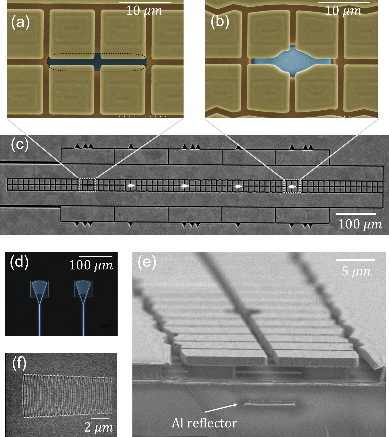
The trap used in this work was designed and fabricated at Sandia National Laboratories using CMOS compatible silicon MEMS fabrication technologies in a configuration similar to those previously reported [20]. Images of the trap are shown in Figure 1. Multiple metal layers are used to route RF and DC signals to electrodes on the top metal level. The top metal layer, containing the RF routing and trap DC control electrodes, overhangs the underlying SiO2 dielectric layer to eliminate direct line of sight between the ion and dielectric. Notable to this particular trap is the integration of silicon nitride waveguides embedded in the SiO2 inter-metal dielectric and routed between metal levels and around vertical electrical vias made of chemical vapor deposited tungsten for delivery of 435 nm light. Light is coupled in and out of the waveguide using diffractive gratings. Figure 1(c) shows the trapping region with a loading hole on the left, and four output gratings to its right. Figure 1(a) shows a zoom-in of the loading hole site, and Figure 1(b) shows a zoom-in of the leftmost output grating site. The small electrodes immediately above and below the trap axis are DC control electrodes. The RF electrodes are the long rails between the DC control electrodes and the outer DC bias electrodes.
Plasma-enhanced chemical vapor deposition (PECVD) silicon nitride waveguides with a thickness of 70 nm were deposited within the 2 m SiO2 dielectric layer between trap metal layers; the silicon nitride layer is kept thin to reduce material absorption. We have observed a propagation loss of -2.5 dB/cm at 435 nm in test waveguides fabricated with similar processes. The input grating (Figure 1(d)) is designed for free space coupling with a relatively large beam waist of 15 m. The output grating (Figure 1(f)) is located between the DC electrodes and designed to produce a beam which focuses at the height of the ion. Utilizing the metal trap routing layer, an Al reflector is positioned below the output grating to increase efficiency (Figure 1(e)).
Simulations of the ideal structure show -6.5 dB input coupling loss and -1.6 dB output coupling loss for an expected total through chip insertion loss of approximately -9.7 dB. The output beam is simulated to emit at a angle with respect to the plane of the chip and have a focused beam waist of 1.45 m at the height of the ion with expected polarization parallel to the chip surface. In a separate die external to the ultra high vacuum chamber trapped ion system we measure a through chip insertion loss of -22 dB and a beam waist of 2.5 m at a height of 20 m above the chip. The difference in the beam waists is likely due to fabrication tolerances, while the difference in through chip insertion loss is likely due to reduced input coupling from a cleaved fiber. In future devices, we plan to use edge coupling instead of the input diffraction grating, which is expected to reduce input coupling loss to -3 dB with a photolithography process and to -0.5 dB with e-beam lithography.
III Experimental details and results
171Yb+ions are produced via an isotope-selective two-photon ionization process [21], Doppler cooled to an average number of quanta quanta, and sideband cooled to achieve as low as 0.1 quanta. An RF voltage at 74.5 MHz is applied to the RF rails (yellow in Figure 1) and quasi-static voltages are applied to electrodes to control the axial position and cancel stray fields. Typical secular axial trap frequencies are tunable between 22.5 and 25.2 MHz and radial trap frequencies are 212.7 MHz. These frequencies are verified via spectroscopy on the to quadrupole clock transition. All beams are delivered via free-space optics with the exception of the 435 nm beam, which addresses the quadrupole transition and can be switched between free-space and waveguide delivery.
III.1 Heating rates
We measure the motional heating rate , or the time rate of change of the average number of quanta for a given motional mode, for the axial trap mode on the to transition by comparing the amplitudes of the red and blue axial sidebands [22]. The transition was chosen because it has the strongest coupling with the freespace beam for our geometry.
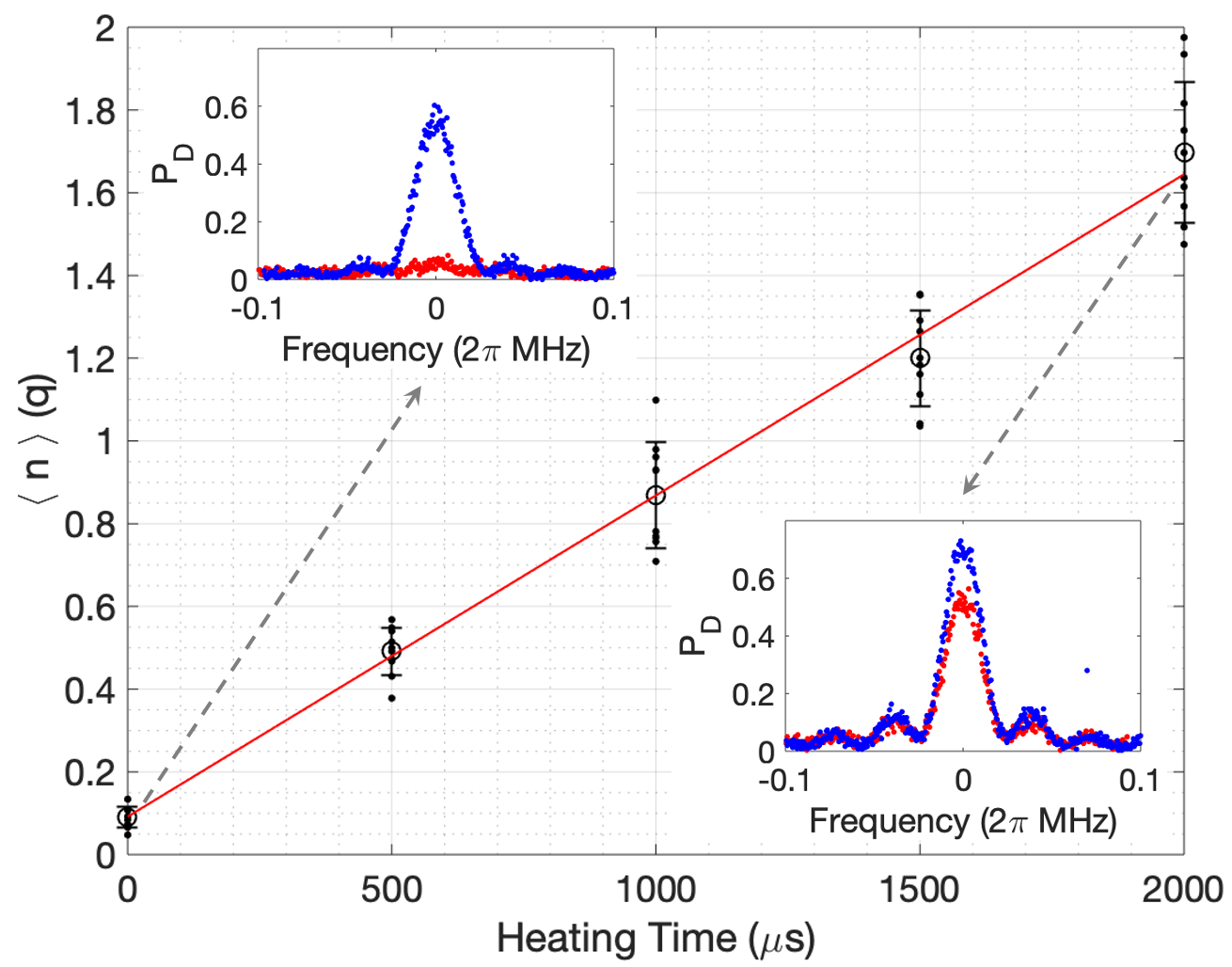
Results of a heating rate measurement taken with the sideband asymmetry method can be seen in Figure 2. After sideband cooling and without any additional heating time, we achieve and the red axial sideband is significantly suppressed. After a heating time of 3 ms, the ion reaches a temperature roughly the same as the Doppler cooling temperature, or quanta, so we limit our heating time in a typical measurement to 2 ms or less, as shown in Figure 2.
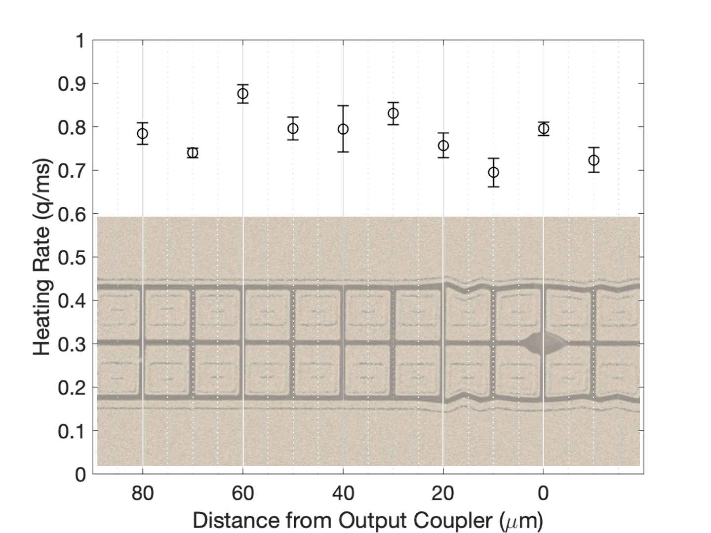
To address the concern of increased heating rates over dielectric materials [17], we shuttle our ion from the loading hole, where it is above bare aluminum electrodes, to a location directly over the output grating of a waveguide. Here the ion is in direct line of sight with the silicon nitride waveguide. Figure 3 shows the heating rate at 10 m increments over a range of 80 m between the loading hole and the dielectric output grating. Remarkably, there is no measurable change in heating rate even when the ion is positioned directly above the dielectric output grating at a height of 20 m. The mean heating rate across the chip is 0.780.05 q/ms.
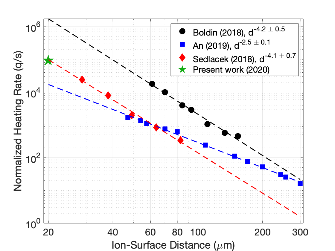
We can normalize our measured heating rate for ion mass and trap frequency to compare with community data [16, 23, 24]. To do so, we consider the heating rate given by where is the charge of the ion, is the mass of the ion, is the motional frequency, and is the spectral density of the electric field noise which goes like . Scaling to MHz and 40Ca+ allows us to compare our data point at 20 m ion-surface distance with published data at larger ion-surface distances. Fig 4 shows that our normalized heating rate falls along the extrapolated scaling found in other experiments [24, 15, 14].
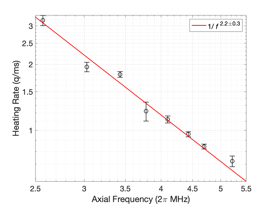
We also measure the heating rate as a function of axial secular trap frequency over the loading hole. Figure 5 shows our results as we scan the frequency from 22.5 to 25.2 MHz. The fitted line represents power law which agrees well with previously reported heating rate trends and is consistent with scaling of electric field spectral density [15, 24].
III.2 Waveguide beam profile
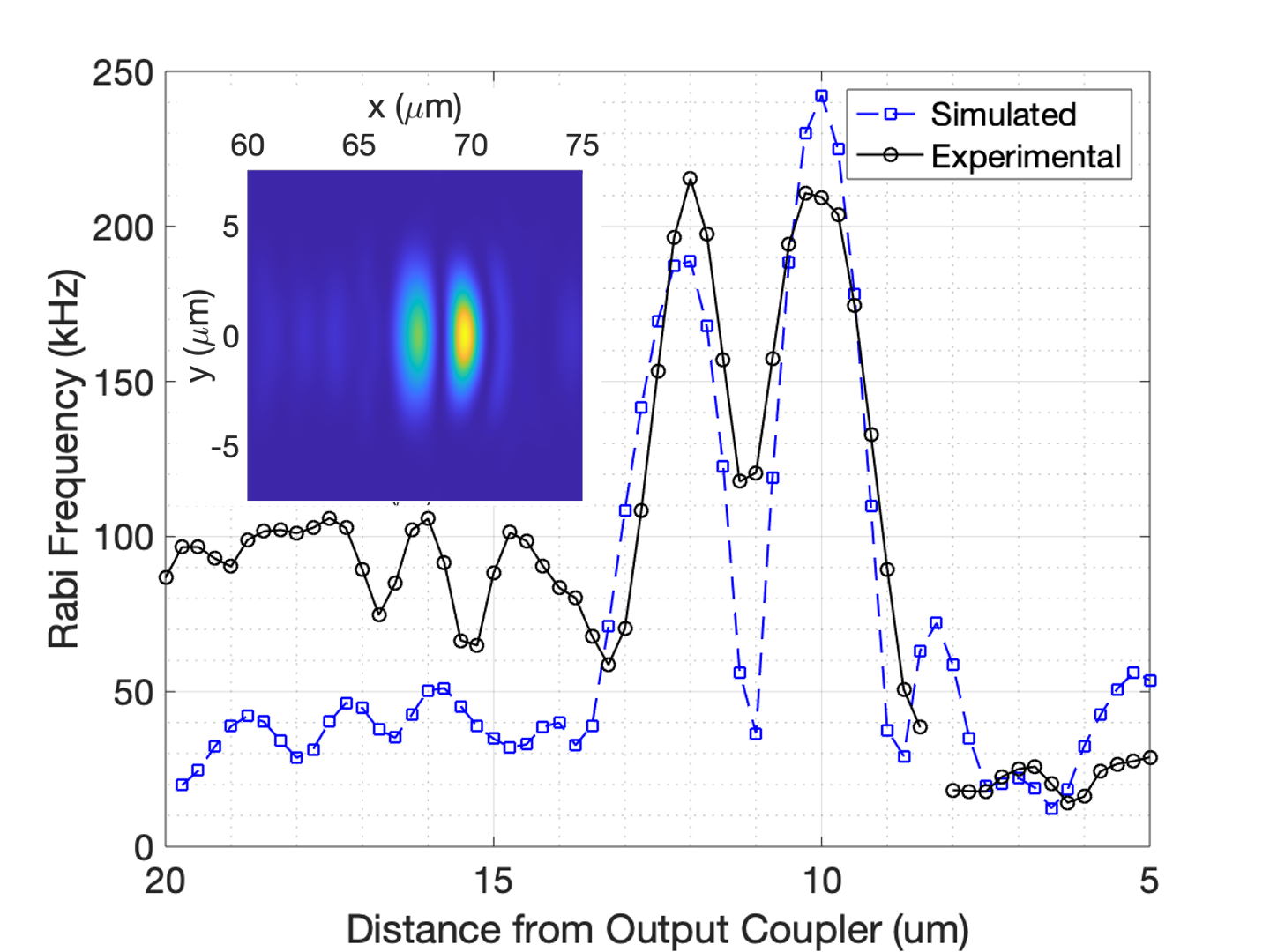
We couple 435 nm light into the waveguide via the input diffraction grating shown in Figure 1d which emits light from the output grating at a measured angle of 66∘ (Figure 1f). This differs from the simulated output angle of 63∘ due to fabrication tolerances. Roughly 26 mW of power is incident on the input grating. We determine the output intensity by measuring the Rabi rate of the ion at various positions around the expected grating output and plot the relative Rabi frequencies as a function of ion position for the transition (see Figure 6). In this device, we observed a double peak profile from the grating. Note the dip in transmission near 11 m from the output grating. We attribute this to destructive interference in the output beam due to variations in the distance between the grating and reflector described in the Trap Design and Fabrication Section. Due to limitations in the fabrication tolerances, there are variations in the oxide thickness across the wafer, and therefore the actual distance between the grating and reflector varies across the wafer. This variation in spacing between grating and reflective surface is a result of the chemical mechanical polishing process which is used to polish the oxide layer above the metal, prior to deposition of the silicon nitride waveguide layer. This process results in variation of the oxide thickness across the wafer on the order of 100 nm.
This double-peak feature was reproduced in simulation by vertically shifting the location of the reflector by 60 nm from the nominal design point, which results in a reduction of the output efficiency from -1.6 dB in the ideal case to -3.7 dB, and two sub-micron peaks separated by 1.8 m. The simulated output intensity profile with this 60 nm shift is shown as a 2D cross section at the anticipated ion height in the Figure 6 inset. The simulated 1D Rabi frequency corresponding to m in the inset is shown in blue in Figure 6.
In future devices the fabrication uncertainty will be reduced by altering the fabrication process such that the thickness of the oxide between the metal reflector and grating are set by a single deposition process, without a polishing step. This is expected to reduce cross-wafer oxide variation below 10 nm and eliminate the double peak in the output profile.
Despite this feature, we have observed -times as fast as 4.130.02 s corresponding to Rabi frequencies as high as kHz when coupling to the waveguide is optimized. This corresponds to an estimated peak intensity of nearly 300 nW/m2 and through-chip coupling of -39 dB.
III.3 Electrostatic charging measurements and results
In some traps with integrated photonics, an ITO coating is deposited over the exposed dielectrics to prevent charge buildup [12]. For our traps, ITO was not employed as it was not compatible with the CMOS facility used at Sandia. Consequently, we observe an effect due to photo-liberated electrons charging the 35 m2 area of exposed dielectric material (corresponding to a 0.31 steradian solid angle) that composes the output grating coupler of the integrated waveguide. The electric field from the charged grating coupler simultaneously shifts the position of the ion and perturbs the harmonic potential of the prescribed trapping fields. We measure this effect by monitoring the axial motional sideband frequency in two different scenarios: 1) Charging is induced via continuously applied light through the waveguide (off-resonant) and the sideband frequency is probed via a free space beam; 2) The charging is induced and the sideband frequency is probed via light coupled through the waveguide. In the latter case, the light through the waveguide is pulsed on only during the probe time, which is more representative of normal operation.
III.3.1 Continuous Photo-induced Charging
We first investigate the photo-induced charging effect at a long timescale by measuring the axial secular frequency with a free-space beam. Using a free space beam to probe the ion allows us to maintain a constant optical power through the waveguide over the duration of the measurement. The secular frequency is measured from the motional sideband of the to transition. This measurement is performed with the ion directly above the grating (80 m from the loading hole in Figure 6). We begin with the waveguide-coupled light shuttered. We interrogate the resonant frequencies of the red and blue axial sidebands approximately every 15 seconds while the waveguide coupler is continuously charged for s by turning on the non-resonant waveguide-coupled light and then discharged for s by turning off the waveguide-coupled light.
The results of the charging experiment are shown in Figure 7. The first s shows the baseline axial frequency after the waveguide has been off for a period of hours. We turn on the waveguide-coupled light at 400 s . The charging is characterized by two main effects. The primary effect is a fast negative charging of the top metal layer. This is attributed to a small electric dipole created when electrons are excited from the metal onto insulating patches of oxide above [25]. This effect is superimposed by a slower secondary effect of positive charging of the dielectric grating. These two effects have been previously observed and are well characterized in similar photo-induced charge studies [25]. When the waveguide-coupled light is turned off at s, both materials slowly discharge.
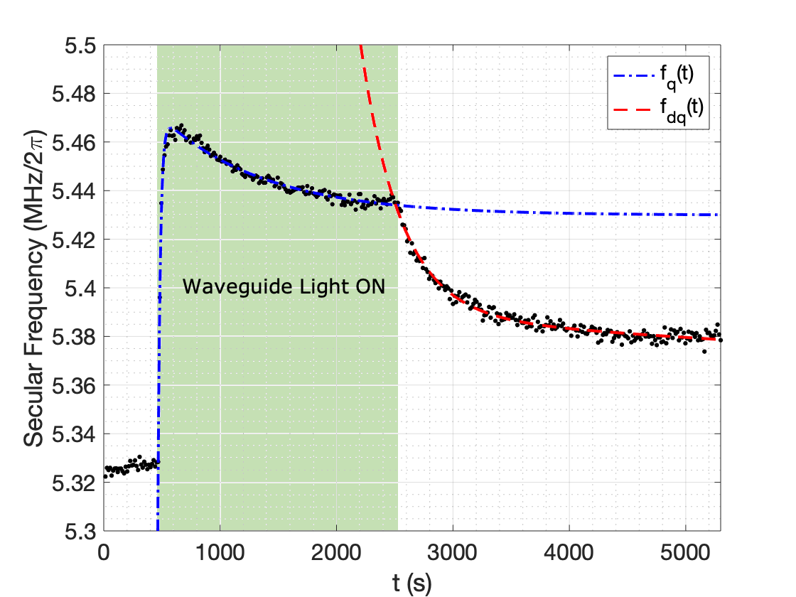
With the light on, the frequency shift due to charging can be fit to the following form:
| (1) | |||||
where are the settling frequency offsets of the two charging effects. The difference represents the settling frequency offset with the waveguide light on. The terms and represent the turn on time of the waveguide light and the charging time, respectively. The initial frequency prior to turning on the waveguide light is .
After the waveguide light has been extinguished, the frequency shift due to discharging can be described as follows:
| (2) | |||||
where and are the settling frequency offsets and the discharging times of the two materials, respectively, and is the turn off time of the waveguide light.
In Figure 7, upon waveguide turn on, the charging happens over s and s and the difference of the settling frequency offsets is kHz. After the waveguide turns off, the discharging times are min and hrs as the frequency is expected to return to its original value of MHz. We can negate the settled frequency offset MHz by applying a 2.4 kV/cm electric field in the vertical direction.
For this experiment, approximately 17 mW of off-resonant 435 nm light is directed on the input coupler to the waveguide. To better understand how much power is coupled through the waveguide, we direct the same amount of power of resonant 435 nm light onto the input coupler and we shuttle the ion 68 m from the loading hole (see Figure 6) where the waveguide outcoupled light is maximally overlapped with the ion. Similar to the beam profile experiments in the Waveguide beam profile subsection, we use the waveguide coupled light to perform Rabi flops on the to transition and achieve -times of 5 s for this particular experiment. Due to the angle of the waveguide beam with respect to our magnetic field, the transition is most strongly coupled by the waveguide beam.
III.3.2 Charging Due to Pulsed Operation
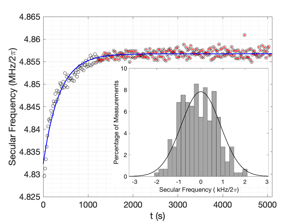
We also monitor the charge-induced frequency shifts using the waveguide coupled light rather than the free-space light in order to determine the stability of the shifted frequency during more typical clock operation. Figure 8 shows the frequency shift of the transition during a typical duty cycle. The charging happens on a much slower timescale because the light is only on for a fraction of the time as the measurements in Figure 7. In these experiments, the waveguide coupled light is only on during probe time for 15 s, which contributes of the duty cycle. A histogram of the difference between the fitted exponential and the data points is shown in the inset for the red points, with a standard deviation of kHz.
IV Conclusion
We have fabricated a surface trap with integrated waveguides for delivering 435 nm light to address the quadrupole transition in 171Yb+. To assess the feasibility of dielectric waveguides in quantum applications, we have characterized the heating rate as a function of proximity to exposed dielectric output grating and of axial secular trap frequency. We see no increase in heating rate over the dielectric, despite having an ion-surface distance of only 20 m. The heating rate scaling with axial secular trap frequency follows a trend consistent with previous results.
We also mapped the output profile of the waveguide by measuring the Rabi frequency of the ion with the waveguide delivered light and showed that it is consistent with simulations and trap fabrication tolerances. We anticipate the beam profile to significantly improve in future devices by eliminating the double-peak feature present in the current device output. Furthermore, transitioning to an edge coupled instead of diffraction grating coupled device at the input is anticipated to improve the input coupling to -3 dB or better, depending on the process used. Despite this feature, we have measured -times as fast as 4.130.02 s.
Finally, we have characterized the electric field shift and stability due to the photo-induced charging of the trap. The lack of deleterious heating over exposed dielectrics or destabilizing photo-induced electric fields is a promising result for the future utilization of these devices in quantum computing and timekeeping applications.
Acknowledgements.
The authors thank the members of Sandia’s Microsystems and Engineering Sciences Application (MESA) facility for their fabrication expertise for helpful comments on the manuscript, as well as H. Haeffner and D. An for their discussions and data for Figure 4. This work was supported by the Defense Advanced Research Projects Activity (DARPA). Sandia National Laboratories is a multimission laboratory managed and operated by National Technology & Engineering Solutions of Sandia, LLC, a wholly owned subsidiary of Honeywell International Inc., for the U.S. Department of Energy’s National Nuclear Security Administration under contract DE-NA0003525. This paper describes objective technical results and analysis. Any subjective views or opinions that might be expressed in the paper do not necessarily represent the views of the U.S. Department of Energy or the United States Government.References
- Stick et al. [2005] D. Stick, W. K. Hensinger, S. Olmschenk, M. Madsen, K. Schwab, and C. Monroe, Ion trap in a semiconductor chip, Nat. Phys. 2, 36 (2005).
- Seidelin et al. [2006] S. Seidelin, J. Chiaverini, R. Reichle, J. J. Bollinger, D. Leibfried, J. Britton, J. H. Wesenberg, R. B. Blakestad, R. J. Epstein, D. B. Hume, W. M. Itano, J. D. Jost, C. Langer, R. Ozeri, N. Shiga, and D. J. Wineland, Microfabricated surface-electrode ion trap for scalable quantum information processing, Phys. Rev. Lett. 96, 253003 (2006).
- Brewer et al. [2019a] S. M. Brewer, J.-S. Chen, A. M. Hankin, E. R. Clements, C. W. Chou, D. J. Wineland, D. B. Hume, and D. R. Leibrandt, quantum-logic clock with a systematic uncertainty below , Phys. Rev. Lett. 123, 033201 (2019a).
- Brewer et al. [2019b] S. M. Brewer, J.-S. Chen, K. Beloy, A. M. Hankin, E. R. Clements, C. W. Chou, W. F. McGrew, X. Zhang, R. J. Fasano, D. Nicolodi, H. Leopardi, T. M. Fortier, S. A. Diddams, A. D. Ludlow, D. J. Wineland, D. R. Leibrandt, and D. B. Hume, Measurements of and magnetic constants for improved ion-clock accuracy, Phys. Rev. A 100, 013409 (2019b).
- Borregaard and Sorensen [2013] J. Borregaard and A.S. Sorensen, Efficient atomic clocks operated with several atomic ensembles, Phys. Rev. Lett. 111, 090802 (2013).
- Mehta et al. [2016] K. Mehta, C. Bruzewicz, R. McConnell, R. J. Ram, J. M. Sage, and J. Chiaverini, Integrated optical addressing of an ion qubit, Nature Nanotechnology 11, 1066 (2016).
- Jiang et al. [2011] L. Jiang, W. B. Whitten, and S. Pau, A planar ion trapping microdevice with integrated waveguides for optical detection, Opt. Express 19, 3037 (2011).
- Slichter et al. [2017] D. H. Slichter, V. B. Verma, D. Leibfried, R. P. Mirin, S. W. Nam, and D. J. Wineland, Uv-sensitive superconducting nanowire single photon detectors for integration in an ion trap, Opt. Express 25, 8705 (2017).
- Mehta et al. [2020] K. Mehta, C. Zhang, M. Malinowski, T.-L. Nguyen, M. Stadler, and J. P. Home, Integrated optical multi-ion quantum logic, Nature 586, 533 (2020).
- West et al. [1998] G. N. West, W. Loh, D. Kharas, C. SoraceAgaskar, K. K. Mehta, J. Sage, J. Chiaverini, and R. J. Ram, Low-loss integrated photonics for the blue and ultraviolet regime, APL Photonics 4, 026101 (1998).
- Sorace-Agaskar et al. [2019] C. Sorace-Agaskar, D. Kharas, S. Yegnanarayanan, R. T. Maxson, G. N. West, W. Loh, S. Bramhavar, R. J. Ram, J. Chiaverini, J. Sage, and P. Juodawlkis, Versatile silicon nitride and alumina integratedphotonic platforms for the ultravioletto short-wave infrared, IEEE Journal of Selected Topics in Quantum Electronics 25, 8201515 (2019).
- Niffenegger et al. [2020] R. J. Niffenegger, J. Stuart, C. Sorace-Agaskar, D. Kharas, S. Bramhavar, C. D. Bruzewicz, W. Loh, R. McConnell, D. Reens, G. N. West, J. M. Sage, and J. Chiaverini, Integrated multi-wavelength control of an ion qubit, Nature 586, 538 (2020).
- Brownnutt et al. [2015] M. Brownnutt, M. Kumph, P. Rabl, and R. Blatt, Ion-trap measurements of electric-field noise near surfaces, Rev. Mod. Phys. 87, 1419 (2015).
- Boldin et al. [2018] I. A. Boldin, A. Kraft, and C. Wunderlich, Measuring anomalous heating in a planar ion trap with variable ion-surface separation, Phys. Rev. Lett. 120, 023201 (2018).
- Sedlacek et al. [2018] J. A. Sedlacek, A. Greene, J. Stuart, R. McConnell, C. D. Bruzewicz, J. M. Sage, and J. Chiaverini, Distance scaling of electric-field noise in a surface-electrode ion trap, Phys. Rev. A 97, 020302(R) (2018).
- Hite et al. [2012] D. A. Hite, Y. Colombe, A. C. Wilson, K. R. Brown, U. Warring, R. Jördens, J. D. Jost, K. S. McKay, D. P. Pappas, D. Leibfried, and D. J. Wineland, 100-fold reduction of electric-field noise in an ion trap cleaned with in situ argon-ion-beam bombardment, Phys. Rev. Lett. 109, 103001 (2012).
- Kumph et al. [2016] M. Kumph, C. Henkel, P. Rabl, M. Brownnutt, and R. Blatt, Electric-field noise above a thin dielectric layer on metal electrodes, New Journal of Physics 18, 023020 (2016).
- Brown et al. [2016] K. R. Brown, J. Kim, and C. Monroe, Co-designing a scalable quantum computer with trapped atomic ions, njp Quantum Inf 2, 16034 (2016).
- Pino et al. [2021] J. M. Pino, J. M. Dreiling, C. Figgatt, J. P. Gaebler, S. A. Moses, C. H.Baldwin, M. Foss-Feig, D. Hayes, K. Mayer, C. Ryan-Anderson, and B. Neyenhuis, Demonstration of the qccd trapped-ion quantum computer architecture, Nature 592, 209 (2021).
- Moehring et al. [2011] D. L. Moehring, C. Highstrete, D. Stick, K. M. Fortier, R. Haltli, C. Tigges, and M. G. Blain, Design, fabrication and experimental demonstration of junction surface ion traps, New Journal of Physics 13, 075018 (2011).
- Johanning et al. [2011] M. Johanning, A. Braun, D. Eiteneuer, C. Paape, C. Balzer, W. Neuhauser, and C. Wunderlich, Resonance-enhanced isotope-selective photoionization of ybi for ion trap loading, App. Phys. B 103, 327 (2011).
- Roos [2000] C. F. Roos, Controlling the quantum state of trapped ions, Ph.D. thesis, University of Innsbruck (2000).
- Noel et al. [2019] C. Noel, M. Berlin-Udi, C. Matthiesen, J. Yu, Y. Zhou, V. Lordi, and H. Haffner, Electric-field noise from thermally activated fluctuators in a surface ion trap, Phys. Rev. A 99, 063427 (2019).
- An et al. [2019] D. An, C. Matthiesen, E. Urban, and H. Haffner, Distance scaling and polarization of electric-field noise in a surface ion trap, Phys. Rev. A 100, 063405 (2019).
- Harlander et al. [2012] M. Harlander, M. Brownnutt, W. Hänsel, and R. Blatt, Trapped-ion probing of light induced charging effects on dielectrics, New J. Phys. 12, 093035 (2012).