Superconducting Transition Temperature Modulation in NbN via EDL Gating
Abstract
We perform electric double-layer gating experiments on thin films of niobium nitride. Thanks to a cross-linked polymer electrolyte system of improved efficiency, we induce surface charge densities as high as cm-2 in the active channel of the devices. We report a reversible modulation of the superconducting transition temperature (either positive or negative depending on the sign of the gate voltage) whose magnitude and sign are incompatible with the confinement of the perturbed superconducting state to a thin surface layer, as would be expected within a naïve screening model.
In recent years, electric double layer (EDL) gating has become a popular tool in condensed matter physics to tune the chemical potential of a wide range of materials well beyond the capabilities of standard solid-gate field-effect devices. Indeed, the EDL that builds up at the interface between the active channel and a polymer electrolyte solution (or an ionic liquid) acts as an effective nanoscale capacitor with extremely high capacitance [1]. In the field of superconductivity, EDL gating has been shown to rival the effects of standard chemical doping in its capabilities to modify the properties of various materials [2]. So far, the attention has been focused on relatively low-carrier-density systems, where the electric field effect is stronger. Superconductivity induced by EDL gating was first reported in undoped SrTiO3 [3], then in ZrNCl [1] and more recently in MoS2 [4]. A Mott-insulator-to-metal transition was induced in the iron chalcogenide TlFe1.6Se2, though the induced carrier density was not sufficient to induce superconductivity [5]. Robust control on the transition temperature of cuprates was also claimed [6, 7, 8].
On the contrary, investigation of the effects of EDL gating on strongly metallic compounds in general, and standard BCS superconductors in particular, has insofar been lacking, probably because the electric field is expected to be strongly screened in such materials. Even so, our earlier experiments on gold [9] and other noble metals [10] have shown that it is possible to obtain reversible resistance modulations as high as 10 % at low temperature in these systems.
Electric field effect in BCS superconductors exploiting a standard gating technique with a solid dielectric [11] or a ferroelectric gating [12] was already investigated in the sixties. Those seminal works showed a small but detectable modulation of the superconducting transition temperature, compatible with the increase/decrease of the density of charge carriers.
In this work, we present the results of field-effect experiments in 40-nm-thick films of the standard strong-coupling electron-phonon superconductor niobium nitride (NbN). With respect to the early papers mentioned above, the use of the EDL technique with a specifically designed cross-linked polymer electrolyte system (PES) allows inducing much higher charge densities. Small, but clearly detectable shifts in the superconducting transition temperature are induced upon electron depletion and accumulation in the active channel of our field-effect devices. The sign of these shifts is in agreement with an electrostatic modulation of the density of states of the material in the vicinity of its unperturbed value. However, a simple naïve model in which the perturbation is confined to the very surface of the film because of Thomas-Fermi screening is absolutely incompatible with the experimental findings, and more complex explanations are necessary to account for the results.
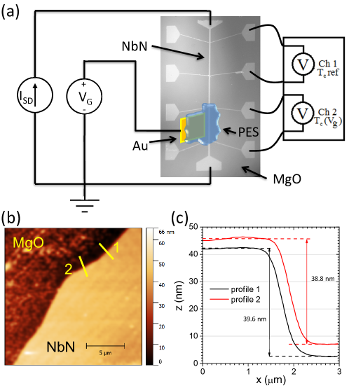
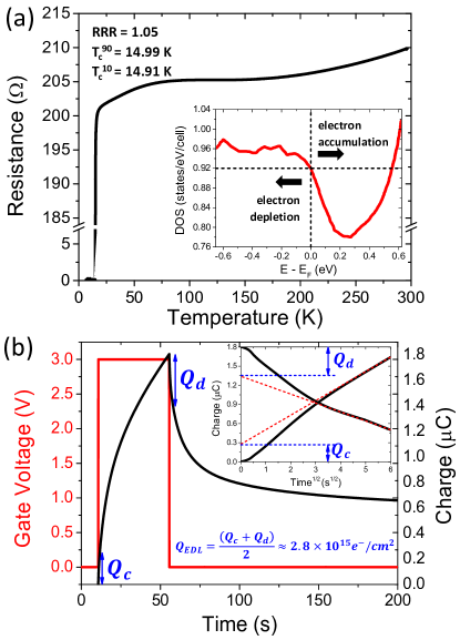
NbN thin films were grown on insulating MgO substrates by reactive magnetron sputtering and were patterned in a Hall-bar geometry by photolithography and wet etching in a 1:1 HF:HNO3 solution. A patterned film is shown in Fig. 1a; the strip is 135 m wide and is divided into three identical, 946 m long “channels” in series (each delimited by adjacent voltage contacts). Surface quality and film thickness were characterized by atomic force microscopy (AFM) after device patterning. Figure 1b shows a 17 17 m2 AFM scan of the edge of the strip. An analysis of the film surface far from the edge shows an average roughness of about 1 nm. Figure 1c shows the z-profile of the film measured along the straight lines crossing the edge shown in panel (b). The film thickness, averaged over several similar cuts in different regions, turns out to be nm. The shape of the sample allows us to measure at the same time the voltage drop (and thus the resistance) across two of the three channels when a dc current ISD flows across the strip, as shown in the sketch of Fig. 1a. The resistance measurements were carried out in a two-stage pulse-tube cryocooler, from 300 K down to 2.7 K. The dc source-drain current ISD was always between 10 and 50 A, which ensures a reliable measurement of without appreciable shifts due to heating or critical current effects. Thermoelectric voltages were eliminated by inverting the current within each measurement [9]. Figure 2a shows the typical curve of any one channel, which exhibits the nonmonotonic behavior characteristic of granular NbN films [13]. The critical temperatures determined at 10 and 90 % of the resistive transition are K and K, respectively. The uncertainties account for the reproducibility of the measurements in different thermal cycles. As discussed elsewhere [13], the residual resistivity ratio indicates that the film quality is fairly high. In any case, the critical temperature of NbN has been proven to be primarily governed by carrier density rather than disorder scattering [14].
After this preliminary characterization of the film, we put the gate electrode (made of a rectangular leaf of gold) on the substrate, adjacent to one of the channels (the “active” channel). The liquid reactive mixture precursor of the PES was then drop-cast on top of the active channel and the neighboring gate, and UV-cured in a dry room. We chose the specific formulation of the PES from our earlier experiments on noble metals [9, 10] owing to its record amount of charge induction: a mixture of bisphenol A ethoxylatedimethacrylate (BEMA) and poly(ethylene glycol) methyl ether methacrylate (PEGMA) in 3:7 ratio, with 10 % wt of lithium bis-trifluoromethanesulfonimide (LiTFSI) and 3 % wt of free radical photo initiator. The area of the Au gate electrode was always larger than that of the active channel, to ensure that the voltage drop across the EDL that forms on the active channel practically coincides with the whole applied gate voltage. In any case, the critical parameter in our experiments is the surface density of induced charges and not the gate voltage.
Field-effect measurements were initially made at room temperature, above the glassy transition of the PES (that occurs below 230 K), to determine the amount of charge induced by a given gate voltage . A source-measure unit (SMU) was used to apply and to measure the gate current; at the same time, we measured the resistance of the active and reference channels. When a positive (negative) gate voltage is applied, two things happen: (i) the gate current shows a peak (dip) and then decreases (increases) finally saturating at an approximately constant value [9]. Even for the maximum gate voltages ( V), this current is 104 times smaller than ; (ii) the active channel resistance shows a decrease (increase) that is perfectly reversible only as long as the gate voltage does not exceed V (for which the relative resistance variation is 0.8 %). Limiting the gate voltage to the range of reversibility ensures that only electrostatic effects are taking place, and allows avoiding unwanted electrochemical reactions at the active channel surface.
The induced charge density was determined by using the well-established electrochemical technique called double-step chronocoulometry (DSCC) [15] based on the fact that the gate current contains two contributions: (which is due to the build-up of the electric double layer and decays exponentially in time) and (which is due to the diffusion of electroreactants and varies with the square root of time). Figure 2b shows the time dependence of the total charge that flows through the gate circuit (obtained by integrating the gate current from zero to ) when a gate voltage is applied and then removed. In the inset, is plotted (separately for the charge and discharge) as a function of . The values of for charge and discharge (called and in Fig. 2b) are determined by the intercept of the asymptotic trends of (dashed lines) [15]. The surface density of charge carriers induced in the active channel is thus given by , where is the elementary charge and is the area of the gated channel [9, 10].
Once the value of corresponding to a given was determined, we cooled down the device keeping constant. Once the base temperature (2.7 K) was reached, the cryocooler was switched off and the curve of both the active and reference channels (ch. 2 and 1 in Fig. 1a) was measured, in quasistatic conditions, during the very slow heating of the device up to room temperature. Using channel 1 as a reference allows detecting the shifts in the of channel 2 with an improved sensitivity ( K) with respect to the absolute measure of itself.
An extensive analysis of the response to the charge induction is beyond the scope of this paper and will be discussed elsewhere. Here, we only note that the amplitude of the shift monotonically increases with , and we limit ourselves to the results obtained for V, i.e., for the highest value of that still ensures reversible effects. In these conditions, the resistance of the active channel is modified by 0.8 % with respect to that of the reference channel but there is no change in the shape of the curve – indeed, the shape is governed by the granular nature of the film and not by the density of charge carriers [13].
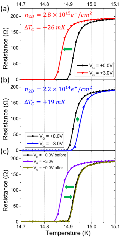
Let us now focus on the region of the superconducting transition. Figure 3a shows the curve of the active channel for (circles) compared to the same curve for V (down triangles) which corresponds to electrons/cm2 according to DSCC. Note that the superconducting transition does not change shape or width, and is simply translated horizontally. In this particular case, the temperature shift is mK. Similarly, Fig. 3b shows the effect of a gate voltage V (corresponding to holes/cm2); in this case, is enhanced by mK. A proof of the fact that these shifts are only due to electrostatic charge induction/depletion and not to chemical reactions, ions adsorption, surface degradation, and so on, is provided in Fig. 3c that shows three subsequent curves measured with , +3.0 V, 0 which clearly demonstrate the complete reversibility of the shift.
The fact that electron accumulation gives rise to a decrease in while electron depletion causes an increase in can be qualitatively explained by looking at the density of states of NbN shown in the inset to Fig. 2a. The DOS was calculated with either the full-potential linearized augmented plane wave method or the pseudopotential method – as implemented in the Elk code (http:// elk.sourceforge.net/) and in the Quantum Espresso package [16]. Around the unperturbed chemical potential , the DOS is asymmetric, i.e., it decreases when the chemical potential is increased (by means of electron accumulation) and vice versa. Within the Eliashberg theory of superconductivity, which is well obeyed by NbN (a standard strong-coupling electron-phonon superconductor with [14]), an increase (decrease) in the density of states at the Fermi level is expected to give rise to an increase (decrease) in .
To calculate the shift of the chemical potential , one needs to know the perturbation in the volume charge density, , but the experimentally accessible quantity is – which is the integral of over the whole film thickness. The simplest, rough approximation for the profile is a Heaviside step function: , being the thickness of the perturbed layer. In NbN, the Thomas-Fermi screening length is of the order of Å, so that it is reasonable to take Å, i.e., equal to the height of one unit cell. The resulting values of are reported in Table 1, as well as the corresponding shifts in the chemical potential . We then solve the Eliashberg equations to calculate the expected of the perturbed layer, assuming that the applied electric field does not affect the phonon spectrum, and modifies the electron-phonon spectral function and the Coulomb pseudopotential only through the DOS modulation.
Table I reports the values of the calculated shifts for V compared to the experimental ones shown in Fig. 3a,b. Although the calculated shifts refer only to the surface layer, nothing changes if the resistance of the whole film is calculated as the parallel of the perturbed and unperturbed layers. It is clear that the calculations completely fail to reproduce the experimental findings. For electron depletion (), is overestimated by a factor . For electron accumulation (), the calculated chemical potential shift is so large that the system crosses the DOS minimum just above , the DOS increases and is hugely enhanced, in complete contrast with the experiment. Clearly, this means that the modulation of the superconducting properties is not limited to a surface layer of the order of one unit cell, as we have initially assumed.
Moreover, if the induced charge density was limited to a surface layer (no matter how thick), there would be no way to detect a suppression of the transition temperature (as we instead do in the case of electron accumulation, see Table 1), since the underlying bulk would still become superconducting at a higher temperature, thus shunting the layer with locally depressed . Such an observation can only be rationalized if the whole film thickness is somehow interested by the shift. Understanding this effect requires a detailed investigation of the capability of the extremely high electric fields generated by EDL gating to penetrate inside a superconductor.
In conclusion, we performed EDL gating experiments on the standard strong-coupling electron-phonon superconductor NbN. Large densities of induced charge were obtained, up to carriers/cm2, with a modulation of the room-temperature resistance up to several parts per thousand. We investigated the effect of the high electric field on the of the material, and found it compatible in sign with small displacements of the chemical potential that would result in changes in the local DOS. However, the magnitude of the shift of is incompatible with a simple parallel-conducting- channel model in which the thickness of the perturbed layer is determined by the Thomas-Fermi screening length. Actually, the observation of a negative shift of seems to indicate that the whole thickness of the film is perturbed. These findings pave the way toward a deeper understanding of the response of standard superconductors to strong electric fields. More generally, they might also help addressing the still pending problem of screening in materials subjected to the extreme conditions reachable in the EDL field-effect devices.
References
- [1] Ye, J.T. et al. Nature Mater. 9, 125–128 (2010).
- [2] Ueno, K. et al. J. Phys. Soc. Jpn. 83, 032001 (2014).
- [3] Ueno, K. et al. Nature Mater. 7, 855–858 (2008).
- [4] Ye, J.T. et al. Science 338, 1193 (2012).
- [5] Katase, T. et al. Proc. Natl. Acad. Sci. U.S.A. 111, 11 (2014).
- [6] Bollinger, A.T. et al. Nature 472, 458–460 (2011).
- [7] Leng, X. et al. Phys. Rev. Lett. 107, 027001 (2011).
- [8] Leng, X. et al. Phys. Rev. Lett. 108, 067004 (2012).
- [9] Daghero, D. et al. Phys. Rev. Lett. 108, 066807 (2012).
- [10] Tortello M., et al. Appl. Surf. Sci. 269, 17 (2013).
- [11] Glover, R.E. & Sherrill, M.D. Phys. Rev. Lett. 5, 248 (1960).
- [12] Stadler, H.L. Phys. Rev. Lett. 14, 979 (1965).
- [13] Nigro, A. et al. Phys. Rev. B 37, 3970 (1998).
- [14] Chockalingam, S.P. et al. Phys. Rev. B 77, 214503 (2008).
- [15] Inzelt, G. Electroanalytical methods. In: Scholz, F. (ed.) Guide to Experiments and Applications. 2nd edn., Ch. II.4 Chronocoulometry, pp. 147–158. Springer (2010).
- [16] Giannozzi, P. et al. J. Phys. Condens. Matter 21, 395502 (2009).