Nanoscale vector electric field imaging using a single electron spin
2 3. Physikalisches Institut, University of Stuttgart, Pfaffenwaldring 57, 70569 Stuttgart, Germany
∗ Corresponding author. Email: marcus.doherty@anu.edu.au)
Abstract
The ability to perform nanoscale electric field imaging of elementary charges at ambient temperatures will have diverse interdisciplinary applications. While the nitrogen-vacancy (NV) center in diamond is capable of high-sensitivity electrometry, demonstrations have so far been limited to macroscopic field features or detection of single charges internal to diamond itself. In this work we greatly extend these capabilities by using a shallow NV center to image the electric field of a charged atomic force microscope tip with nanoscale resolution. This is achieved by measuring Stark shifts in the NV spin-resonance due to AC electric fields. To achieve this feat we employ for the first time, the integration of Qdyne with scanning quantum microscopy. We demonstrate near single charge sensitivity of charges/, and sub-charge detection (). This proof-of-concept experiment provides the motivation for further sensing and imaging of electric fields using NV centers in diamond.
Electrical phenomena are ubiquitous within the physical sciences. The ability to image electric fields is therefore fundamentally important with diverse interdisciplinary applications. Consequently, a myriad of techniques have been developed for precision electrometry. These have demonstrated nanoscale spatial resolution [1, 2, 3, 4], elementary charge detection [1, 2, 5, 6, 7, 8, 9, 10, 11], and the ability to operate at ambient temperatures and pressures [9, 11]. However, no device currently possesses all three of these properties simultaneously. A device capable of nanoscale imaging of elementary charges at room temperature would offer unparalleled insight into a variety of systems previously inaccessible to existing electrometers. For example, as a critical characterization tool for two-dimensional electronics. These materials promise a flexible low-energy electronic revolution. Since they are only atomically thick, high-precision field-imaging of single electrons/holes at ambient conditions is required to provide insight into their performance and function, but their charge transport properties are often strongly temperature dependent [12, 13]. Enhanced electrometers may also have applications in imaging chemical processes (e.g., photosynthesis) and charge phenomena in biological systems (e.g., neuron firing [14]) that are only relevant at ambient conditions.
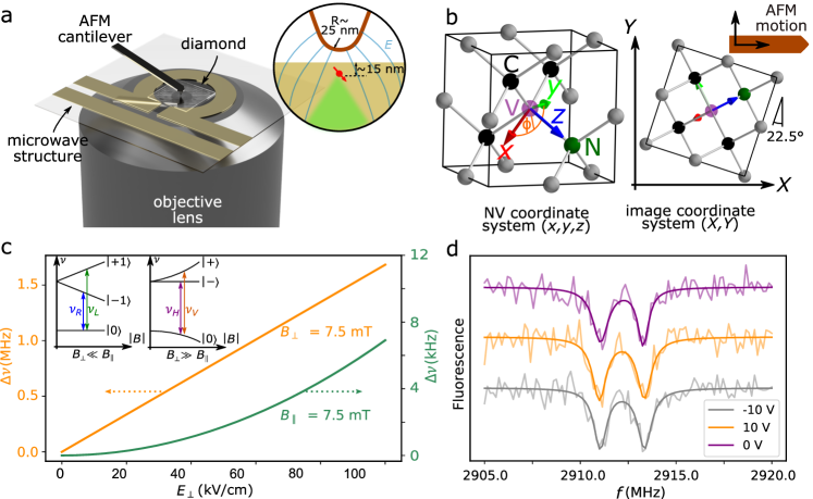
The nitrogen-vacancy (NV) center in diamond [15] is currently the only system capable of imaging elementary charges at room temperatures with nanoscale precision. Single defects have demonstrated impressive AC (DC) electric-field sensitivities of 202 (891 ) [16] while ensemble measurements have achieved shot-noise limited AC sensitivities on the order of 1 [17]. However, these results are limited to detection of macroscopic electric field features [16, 17] or charges internal to diamond [18, 19]. In this work we greatly extend these capabilities by using a single NV center to perform nanoscale electric field imaging of an external source in ambient conditions. A shallow NV center is used to detect the vector components of the electric field produced by the charged tip of an atomic force microscope in contact mode with the diamond surface (figure 1a). Imaging is then realized through nanoscale control of the AFM tip position relative to the NV center.
We achieve these results by exploiting the NV center’s unique capabilities for quantum sensing. These include a bright optical fluorescence, a mechanism for optical spin initialization and readout, and the longest room-temperature coherence time for any solid state spin [15, 20]. The combination of these properties allow for single defect identification and high-fidelity measurement of individual spin-resonances. These properties have previously been applied for precision nano-magnetometry [21, 22], thermometry [23, 24, 25] and quantum computing [26]. Electrometry is realized by measuring the Stark shift of the NV- spin-triplet ground state through optically detected magnetic resonance[16].
The Hamiltonian describing the ground state spin of the NV center in the presence of magnetic () and electric field () is [15]
| (1) |
where GHz is the zero-field splitting [27], Hz/(V/cm) and Hz/(V/cm) are the electric field susceptibility parameters [28] in the axial and transverse NV directions, MHz/mT is the NV spin’s gyromagnetic ratio [27], and are the NV spin-operators (). Analysis of the Hamiltonian (1) reveals that the electric field susceptibility is maximised when the magnetic field is aligned perpendicular to the NV axis [29], as shown in figure 1c. In such a case, the spin resonance frequencies due to the applied electric field are given by
| (2) |
where , , and . Here are the spin-resonances in the absence of the applied electric field. Uniquely, the NV doesn’t sense a potential, charge, capacitance or an electric force like other methods but the measures the electric field directly. Furthermore, the electric field components and the electric field polar angle are immediately separable by varying .
As shown in figure 1d, we were unable to see a Stark shift of the spin-resonances when applying a DC voltage to the tip up to V. This is consistent with existing theory that suggests mobile charges on the diamond surface causes significant screening of DC fields [30]. In contrast, significant Stark shift were observed at AC frequencies even at low voltages ( V). This frequency dependence of the surface screening is not unsurprising, as the finite mobility of charges on the surface will limit screening at higher frequencies.
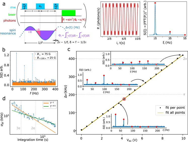
Due to the long time required to raster an image using single point measurements, it is desirable to have as fast as possible measurement time per pixel. For AC frequency measurements, a considerable increase in speed and signal-to-noise can be obtained using the so-called ‘Qdyne’ sensing method [31, 32, 33]. Here our spin-measurements perform like a lock-in amplifier, where we use a known reference signal which is phase referenced to our acquisition system. This reference signal could be the movement of the oscillating AFM cantilever or a time-varying voltage applied to the AFM cantilever. This is the first time Qdyne has been incorporated with scanning probe microscopy. In this work we always apply a time varying voltage to an AFM cantilever in contact mode which introduces a time-varying shift of the spin-resonance of . For imaging, we are interested in detecting the amplitude of this signal (and therefore ) as a function of space.
As shown in figure 2a, by setting the time spacing () of our -pulses to be slightly de-tuned from our applied signal frequency () we obtain a time-dependent fluorescence oscillating at a frequency given by that de-tuning (). If the signal amplitude produces large rotations of the qubit vector about the Bloch sphere () during the phase accumulation, then higher order odd harmonics () in the fluorescence signal become apparent. Qdyne has the benefit of mixing these harmonics down from the AC signal frequency to the detuning frequency making them substantially easier to observe.
Analysis of these harmonics allows us to greatly extend the dynamic range of our amplitude measurement, effectively unwrapping multiple rotations of the Bloch sphere. This is particularly important in imaging where the field magnitude near a source can vary sharply (e.g. ). Additionally, provided at least the second harmonic is present, this can be used to calibrate the signal magnitude using only the information from the signal itself. The specific amplitudes of the harmonics is dependent on the exact rotation of the qubit vector about the Bloch sphere. This self-calibration means that characterization of the optical emission, spin-contrast and other experimental parameters are not required.
An example of this extraction and linearization is shown in figure 2c. Here we have used the power spectrum to analyze the magnitude of the signal harmonics, their relationship with the applied signal amplitude is well defined and can be used to easily extracted the absolute frequency shift due to the applied electric field (see supplementary information for detailed derivation of the Qdyne sensing method).
The standard deviation in the extracted frequency shift for increasing averaging time shows the normal shot-noise dependence, we obtain an signal standard deviation of about 4 kHz after 11 seconds of averaging, giving us a frequency shift sensitivity of 13 kHz. This value just represents the achievable signal given our noise, the real sensitivity to a source external to the diamond is dependent on the extent of the surface screening. Looking at the voltage applied to the AFM tip in figure 2c shows a linear trend of 42 kHz frequency shift per volt, given our frequency shift sensitivity we obtain an AC voltage sensitivity of 0.31 V. Bear in mind, this is strongly dependent on the location of the AFM tip relative to the NV, so it could be in principle improved. Modeling the AFM tip as a conducting sphere of radius 25 nm ( AFM tip radius) with a single charge in the center, gives us an AC charge sensitivity of charges. Therefore, we can detect the potential on the sphere equivalent to a single fundamental charge after 28 seconds of measurement. The longest measurement performed was for 60 seconds, indicating that we measured the signal equivalent to 0.68% of a single elementary charge. As expected, and as shown in figure 2b we do not see an electrometry signal from an AC electric field when the magnetic field is not applied in a direction perpendicular to the NV axis.
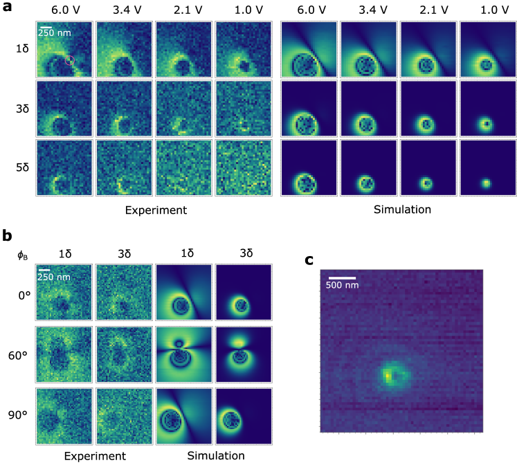
To perform imaging, the same measurement sequence is continuously applied whilst moving the position of the AFM tip relative to the NV in an XY raster motion. The same spectral analysis is then performed in a per pixel manner to extract electric field images. Figure 3 compares the electric field signal from various applied voltages for the first few spin-resonance harmonics to a COMSOLTM simulation of the electric field from an AFM tip (see supplementary information). Note that this COMSOLTM model is very well approximated by the field from a single monopole, as expected from a sharp point or a small conducting sphere at a set potential. We see very strong agreement of an image that corresponds to an NV at a distance 15 nm from the diamond surface and an AFM height of 30 nm above the surface, this height offset was probably from some contaminants on the surface of the diamond, most likely objective lens immersion oil. In this analysis we have ignored the effect of the electric field component as it contributes only about 2% to the NV spin frequency shift. The lobed patterns and asymmetry in these images is due to the projection of the spherically symmetric monopole field from the AFM tip onto the plane transverse to the NV axis. The zero amplitude line that separates the two lobes is where passes through zero.
The effect of rotating the polar field angle is shown in figure 3b. Rotating adds an effective offset to , similar to rotating the NV axis or diamond in the azimuthal direction, in the images this is seen as a rotation of the two lobes. This can be used as a handle to separate and the individual vector components of the electric field and . We can also perform the reverse, and use a model of the electric field to extract the exact NV orientation (see supplementary information). We determine the exact orientation of the NV axes and ordering of the N and V along NV axis, as shown in figure 1b. This is not possible without the application of an electric field [29]. The 0° and 90° images are similar because of the periodicity of . However, when rotating the transverse field by 90°, the polarization of the spin-resonance flips (i.e. the lower/upper spin resonances flip from H/V polarized transitions), Since our microwaves were linearly polarized along only one direction, the 90° image was taken using the lower spin-resonance () and 0° was taking using the upper spin-resonance (). In each case, the microwave power was adjusted such that the Rabi frequency matched between each image. Technically, using the other spin-resonance branch will flip the sign of the interaction in equation (2), but since we are looking at the magnitude of the interaction only, this is not noticed.
The limit for the spatial resolution of this method has not been reached, any AFM or NV position drifts or deformities of the AFM tip geometry could limit our achievable resolution. However, we can see features in figure 3a which are pixel-size limited putting an upper bound on our spatial resolution of 33.3 nm, which could be in principle improved by simply decreasing the image pixel size.
Very close to the AFM tip ( nm) we see quenching of the NV fluorescence (Fig. 3c)), it is expected that this is a plasmonic quenching effect [34]. This could be alleviated by raising the AFM tip slightly off the surface of the diamond or changing to imaging a non-plasmonic sample. It does however provide a useful reference to find the position of the AFM tip relative the image axes. When the AFM tip is further from the NV, the NV fluorescence shows weak concentric rings of weak Purcell enhancement and quenching of the NV fluorescence. These effects are captured from the total NV fluorescence and are included into the analysis of the spin-signal images.
Further work will perform spectroscopy on charge trap mobility using the NV center in diamond to unlock information about the electrical properties of diamond surfaces. This understanding will allow us to limit surface screening to enhance NV electrometry and sensitivity. Additionally, electric field noise from the surface is suspected as a major factor in spin-decoherence for near-surface NV centers [35, 36], greater understanding of the surface will be valuable in mitigating decoherence for shallow NV centers, vitally important for nanoscale imaging and sensing.
Due to the strong electric-field screening at DC we have only demonstrated sensing of AC signals[30]. Limitations of our equipment restricted DC voltages that could be applied to our tip to V. It has recently been demonstrated that DC screening effects can be circumvented at higher voltages[bian2020nanoscale], presumably through saturating charge traps local to the tip and NV. However, the sensitivity of such measurements is limited by the reduced coherence time of the NV center at DC. We instead propose imaging a DC electric field source (e.g. a static charge) through motion of the AFM cantilever (or diamond probe) to add an AC component. In this case the periodic cantilever motion could be used simultaneously as the Qdyne reference signal. We have tested this method with a mechanically oscillating magnetic AFM cantilever and confirmed that the phase/frequency of the AFM motion is stable enough to perform Qdyne (see supplementary information).
In conclusion, we have demonstrated sensitive nanoscale imaging of the electric fields produced from a a voltage on an AFM tip very near a single NV. We see strong screening of the electric field at DC but significant AC fields. This is also the first research presented in the literature where AC electric fields have been sensed using an NV center. We describe and utilize the repetitive readout method ‘Qdyne’ to greatly enhance our signal and imaging acquisition time and amplitude dynamic range, important for imaging a source with strong amplitude gradients. We demonstrate a charge sensitivity of charges/. We see strong agreement with resulting images and the model of the field from an AFM tip. In doing this we isolate the exact NV orientation and perform a demonstration of the vector imaging capability of this method. This work demonstrates that electric field vector imaging with single charge resolution is possible, and will pave the way for exciting new progress in measuring the fields from important nanoscale physical systems in ambient conditions.
Methods
The diamond sample is a 220.03 mm CVD electronic grade diamond membrane with a surfaces that has undergone oxygen plasma surface termination, the NV we focused on was created by 10 keV implantation of nitrogen ions giving an estimated depth of 15 nm 5 nm [37]. We imaged though the diamond, so the NV centers are near the surface furthest from the objective lens and closest to the AFM. The sample was placed on a 0.17 mm thick glass cover slip with a Cu microwave waveguide deposited directly onto the glass. This was sufficient to achieve MHz electron spin Rabi frequencies. This sample had NV centers that generally exhibited electron spin coherence times s and s, but this deteriorated with the applied transverse magnetic field as spin-revivals from the nitrogen hyperfine field limits the usable electron spin evolution time to s for the field strengths used here. This effect is more pronounced for 15N NV centers than for 14N, as the zero-field splitting quadrupole moment of the 14N is large compared to the off diagonal components of the hyperfine interaction [38]. This effect is reduced for smaller magnetic field strengths, but large field strengths are desired to separate the spin resonance by more than our Rabi frequency, in general we apply transverse magnetic field strengths G. This problem could easily be circumvented by controlling the microwave polarization for selective spin resonance control.
Measurements were performed on an inverted confocal microscope/atomic force microscope (Asylum Research MFP3D-Bio). The confocal microscope had a scanning objective lens (Nikon TIRF 1.45/60x). The AFM has its own scanning sample stage where the diamond is placed, as such, the NV center in the diamond has to be followed by the confocal scanning stage as the AFM scanner rasters an image. Excitation was with a 532 nm (Laser Quantum GEM) laser intensity modulated by a 200 MHz AOM, with gating provided by an RF switch. Fluorescence was coupled into a 25 m core fiber and detected using a Excilitas single photon detector (SPCM-AQRH-14-FC). Microwaves were provided by a R&S SMIQ03B signal generator with the XY phase component amplitude modulation from the internal I/Q modulator and amplified with a Minicircuits ZHL-16-43-S+ power amplifier. The electric field signal was provided from a Cr/Pt coated conducting AFM tip (Budget Sensors ElectriCont-G) in contact mode. The electric voltage signal was provided from a Stanford DS345 signal generator and connected via the MFP3D ‘chip’ crosspoint switch terminal. The timing of the photon arrivals was measured using a Swabian Instruments TimeTagger 20. Pulses controlling the AOM switch and XY microwave modulation was from a Swabian Instrument PulseStreamer 8/2. The TimeTagger, PulseStreamer, Stanford DS345 and SMIQ03B were all referenced to the SMIQ03B’s internal 10 MHz reference clock. Vector magnetic field control is provided from a home build electromagnet based on a steel magnetic circuit arrangement placed around the confocal objective lens. This magnet is capable of generating G independently in each axis (XYZ).
Acknowledgments
This work was supported in part by the Australian Research Council (ARC) and European Union research funding. M.W.D. acknowledges the ARC funding DP170102735. J.W. acknowledges funding from ASTERIQS and SMel (ERC grant number: 742610).
Contributions
All experiments and data analysis was performed by M.S.J.B. Experimental apparatus was built by M.S.J.B. COMSOL modeling and analysis was performed by L.M.O. The diamond sample was provided by A.D. and J.W. Advice and guidance provided by L.P.McG, N.B.M. and project leadership from J.W. and M.W.D. All authors contributed to the manuscript with the initial draft written by M.S.J.B. and L.M.O.
References
- [1] M. J. Yoo, T. A. Fulton, H. F. Hess, R. L. Willett, L. N. Dunkleberger, R. J. Chichester, L. N. Pfeiffer, and K. W. West. Scanning single-electron transistor microscopy: Imaging individual charges. Science, 276(5312):579–582, 1997.
- [2] J. Martin, N. Akerman, G. Ulbricht, T. Lohmann, J. H. Smet, K. von Klitzing, and A. Yacoby. Observation of electron-hole puddles in graphene using a scanning single-electron transistor. Nature Physics, 4(2):144–148, 2008.
- [3] Albert K. Henning, Todd Hochwitz, James Slinkman, James Never, Steven Hoffmann, Phil Kaszuba, and Charles Daghlian. Two‐dimensional surface dopant profiling in silicon using scanning kelvin probe microscopy. Journal of Applied Physics, 77(5):1888–1896, 1995.
- [4] C. C. Williams, J. Slinkman, W. P. Hough, and H. K. Wickramasinghe. Lateral dopant profiling with 200 nm resolution by scanning capacitance microscopy. Applied Physics Letters, 55(16):1662–1664, 1989.
- [5] M. H. Devoret and R. J. Schoelkopf. Amplifying quantum signals with the single-electron transistor. Nature, 406(6799):1039–1046, 2000.
- [6] C. Schönenberger and S. F. Alvarado. Observation of single charge carriers by force microscopy. Phys. Rev. Lett., 65:3162–3164, Dec 1990.
- [7] Y. Martin, D. W. Abraham, and H. K. Wickramasinghe. High‐resolution capacitance measurement and potentiometry by force microscopy. Applied Physics Letters, 52(13):1103–1105, 1988.
- [8] A. N. Cleland and M. L. Roukes. A nanometre-scale mechanical electrometer. Nature, 392(6672):160–162, 1998.
- [9] J. Scott Bunch, Arend M. van der Zande, Scott S. Verbridge, Ian W. Frank, David M. Tanenbaum, Jeevak M. Parpia, Harold G. Craighead, and Paul L. McEuen. Electromechanical resonators from graphene sheets. Science, 315(5811):490–493, 2007.
- [10] J. Salfi, I. G. Savelyev, M. Blumin, S. V. Nair, and H. E. Ruda. Direct observation of single-charge-detection capability of nanowire field-effect transistors. Nature Nanotechnology, 5(10):737–741, 2010.
- [11] J. Lee, Y. Zhu, and A. Seshia. Room temperature electrometry with SUB-10 electron charge resolution. Journal of Micromechanics and Microengineering, 18(2):025033, jan 2008.
- [12] S. Ghatak, A. N. Pal, and A. Ghosh. Nature of electronic states in atomically thin mos2 field-effect transistors. ACS Nano, 5(10):7707–7712, 2011. PMID: 21902203.
- [13] K. S. Novoselov, A. K. Geim, S. V. Morozov, D. Jiang, Y. Zhang, S. V. Dubonos, I. V. Grigorieva, and A. A. Firsov. Electric field effect in atomically thin carbon films. Science, 306(5696):666–669, 2004.
- [14] L. Hanlon, V. Gautam, J. D. A. Wood, P. Reddy, M. S. J. Barson, M. Niihori, A. R. J. Silalahi, B. Corry, J. Wrachtrup, M. J. Sellars, V. R. Daria, P. Maletinsky, G. J. Stuart, and M. W. Doherty. Diamond nanopillar arrays for quantum microscopy of neuronal signals. Neurophotonics, 7(3):1 – 12, 2020.
- [15] M. W. Doherty, N. B. Manson, P. Delaney, F. Jelezko, J. Wrachtrup, and L. C. L. Hollenberg. The nitrogen-vacancy colour centre in diamond. Physics Reports, 528(1):1–45, 2013.
- [16] F. Dolde, H. Fedder, M.W. Doherty, T. Nöbauer, F. Rempp, G. Balasubramanian, T. Wolf, F. Reinhard, L.C.L. Hollenberg, F. Jelezko, and J Wrachtrup. Electric-field sensing using single diamond spins. Nature Physics, 7(6):459–463, 2011.
- [17] E. H. Chen, H. A. Clevenson, K. A. Johnson, L. M. Pham, D. R. Englund, P. R. Hemmer, and D. A. Braje. High-sensitivity spin-based electrometry with an ensemble of nitrogen-vacancy centers in diamond. Phys. Rev. A, 95:053417, May 2017.
- [18] F. Dolde, M. W. Doherty, J. Michl, I. Jakobi, B. Naydenov, S. Pezzagna, J. Meijer, P. Neumann, F. Jelezko, N. B. Manson, and J. Wrachtrup. Nanoscale detection of a single fundamental charge in ambient conditions using the center in diamond. Phys. Rev. Lett., 112:097603, Mar 2014.
- [19] T. Mittiga, S. Hsieh, C. Zu, B. Kobrin, F. Machado, P. Bhattacharyya, N. Z. Rui, A. Jarmola, S. Choi, D. Budker, and N. Y. Yao. Imaging the local charge environment of nitrogen-vacancy centers in diamond. Phys. Rev. Lett., 121:246402, Dec 2018.
- [20] E. D. Herbschleb, H. Kato, Y. Maruyama, T. Danjo, T. Makino, S. Yamasaki, I. Ohki, K. Hayashi, H. Morishita, M. Fujiwara, and N. Mizuochi. Ultra-long coherence times amongst room-temperature solid-state spins. Nature Communications, 10(1):3766, 2019.
- [21] G. Balasubramanian, IY Chan, R. Kolesov, M. Al-Hmoud, J. Tisler, C. Shin, C. Kim, A. Wojcik, P.R. Hemmer, A. Krueger, et al. Nanoscale imaging magnetometry with diamond spins under ambient conditions. Nature, 455(7213):648–651, 2008.
- [22] J.M. Taylor, P. Cappellaro, L. Childress, L. Jiang, D. Budker, PR Hemmer, A. Yacoby, R. Walsworth, and M.D. Lukin. High-sensitivity diamond magnetometer with nanoscale resolution. Nature Physics, 4(10):810–816, 2008.
- [23] G. Kucsko, P.C. Maurer, N.Y. Yao, M. Kubo, H.J. Noh, P.K. Lo, H. Park, and M.D. Lukin. Nanometre-scale thermometry in a living cell. Nature, 500(7460):54–58, 2013.
- [24] P. Neumann, I. Jakobi, F. Dolde, C. Burk, R. Reuter, G. Waldherr, J. Honert, T. Wolf, A. Brunner, J.H. Shim, et al. High precision nano scale temperature sensing using single defects in diamond. Nano letters, 2013.
- [25] D.M. Toyli, D.J. Christle, A. Alkauskas, B.B. Buckley, C.G. Van de Walle, and D.D. Awschalom. Measurement and control of single nitrogen-vacancy center spins above 600 k. Physical Review X, 2(3):031001, 2012.
- [26] L. Childress and R. Hanson. Diamond nv centers for quantum computing and quantum networks. MRS Bulletin, 38(2):134–138, 2013.
- [27] J.H.N. Loubser and J.A. Van Wyk. Optical spin-polarisation in a triplet state in irradiated and annealed type 1b diamonds. Diamond Research, pages 11–14, 1977.
- [28] E. Van Oort and M. Glasbeek. Electric-field-induced modulation of spin echoes of nv centers in diamond. Chemical Physics Letters, 168(6):529–532, 1990.
- [29] M. W. Doherty, J. Michl, F. Dolde, I. Jakobi, P. Neumann, N. B. Manson, and J. Wrachtrup. Measuring the defect structure orientation of a single nv-1 centre in diamond. New Journal of Physics, 16(6):063067, 2014.
- [30] L. M. Oberg, M. O. de Vries, L. Hanlon, K. Strazdins, M. S. J. Barson, M. W. Doherty, and J. Wrachtrup. Solution to Electric Field Screening in Diamond Quantum Electrometers. Phys. Rev. Applied, 14(1):14085, jul 2020.
- [31] S. Schmitt, T. Gefen, F. M. Stürner, T. Unden, G. Wolff, C. Müller, J. Scheuer, B. Naydenov, M. Markham, S. Pezzagna, J. Meijer, I. Schwarz, M. Plenio, A. Retzker, L. P. McGuinness, and F. Jelezko. Submillihertz magnetic spectroscopy performed with a nanoscale quantum sensor. Science, 356(6340):832–837, 2017.
- [32] J. M. Boss, K. S. Cujia, J. Zopes, and C. L. Degen. Quantum sensing with arbitrary frequency resolution. Science, 356(6340):837–840, 2017.
- [33] K. Mizuno, H. Ishiwata, Y. Masuyama, T. Iwasaki, and M. Hatano. Simultaneous wide-field imaging of phase and magnitude of ac magnetic signal using diamond quantum magnetometry. Scientific Reports, 10(1):11611, 2020.
- [34] J. R. Lakowicz. Radiative decay engineering 5: metal-enhanced fluorescence and plasmon emission. Analytical biochemistry, 337(2):171–194, 2005.
- [35] M. Kim, H. J. Mamin, M. H. Sherwood, K. Ohno, D. D. Awschalom, and D. Rugar. Decoherence of near-surface nitrogen-vacancy centers due to electric field noise. Phys. Rev. Lett., 115:087602, Aug 2015.
- [36] B. A. Myers, A. Ariyaratne, and A. C. Bleszynski Jayich. Double-quantum spin-relaxation limits to coherence of near-surface nitrogen-vacancy centers. Phys. Rev. Lett., 118:197201, May 2017.
- [37] S. Pezzagna, B. Naydenov, F. Jelezko, J. Wrachtrup, and J. Meijer. Creation efficiency of nitrogen-vacancy centres in diamond. New Journal of Physics, 12(6):065017, 2010.
- [38] L. Childress, M.V.G. Dutt, JM Taylor, AS Zibrov, F. Jelezko, J. Wrachtrup, PR Hemmer, and MD Lukin. Coherent dynamics of coupled electron and nuclear spin qubits in diamond. Science, 314(5797):281–285, 2006.