S
[a]MarkusKustermarkus.kuster@xfel.eu Ahmed Ballak Danilevski\aufnOn leave from the European XFEL, Schenefeld, Germany Ekmedžić Fernandes Gessler Hartmann Hauf Holl Meyer Montaño Münnich Ovcharenko Rennhack Rüter Rupp Schlosser Setoodehnia Schmitt Strüder Tanyag Ulmer Yousef
[a]European XFEL, Holzkoppel 4, \city22869 Schenefeld \countryGermany \aff[b]PNSensor GmbH, Otto-Hahn-Ring 6, \city81739 München \countryGermany \aff[c]Max-Born-Institute, Max-Born-Straße 2A, \city12489 Berlin \countryGermany \aff[d]LFKP. ETH Zürich, John-von-Neumann-Weg 9, \city8093 Zürich \countrySwitzerland \aff[e]IOAP, Technische Universität Berlin, Hardenbergstraße 36, \city10623 Berlin\countryGermany
The 1-Megapixel pnCCD Detector for the Small Quantum Systems Instrument at the European XFEL: System and Operation Aspects
Abstract
The X-ray free-electron lasers that became available during the last decade, like the European XFEL (EuXFEL), place high demands on their instrumentation. Especially at low photon energies below , detectors with high sensitivity, and consequently low noise and high quantum efficiency, are required to enable facility users to fully exploit the scientific potential of the photon source. A 1-Megapixel pnCCD detector with a pixel format has been installed and commissioned for imaging applications at the Nano-Sized Quantum System (NQS) station of the Small Quantum System (SQS) instrument at EuXFEL. The instrument is currently operating in the energy range between and and the NQS station is designed for investigations of the interaction of intense FEL pulses with clusters, nano-particles and small bio-molecules, by combining photo-ion and photo-electron spectroscopy with coherent diffraction imaging techniques. The core of the imaging detector is a pn-type charge coupled device (pnCCD) with a pixel pitch of . Depending on the experimental scenario, the pnCCD enables imaging of single photons thanks to its very low electronic noise of and high quantum efficiency. Here we present an overview on the EuXFEL pnCCD detector and the results from the commissioning and first user operation at the SQS experiment in June 2019. The detailed descriptions of the detector design and capabilities, its implementation at EuXFEL both mechanically and from the controls side as well as important data correction steps aim to provide useful background for users planning and analyzing experiments at EuXFEL and may serve as a benchmark for comparing and planning future endstations at other FELs.
keywords:
X-ray Detectorkeywords:
Photon Detectionkeywords:
pnCCDkeywords:
X-ray CCDkeywords:
Free Electron LaserA description of the 1-Megapixel pnCCD detector design and capabilities, its implementation at EuXFEL’s Small Quantum Systems Instrument both mechanically and from the controls side as well as important data correction steps aim to provide useful background for users planning and analyzing experiments at EuXFEL and may serve as a benchmark for comparing and planning future endstations at other FELs.
1 Introduction
The increasing availability of X-ray free-electron laser (FEL) sources [Altarelli:2006a, Emma:2010a, Ganter:2010a, Ishikawa:2012a, Kang:2017a] over the last decade has triggered various new developments and improvements in spectrometer and detector technologies in order to enable the scientific community to fully exploit the capabilities of these sources for experimental investigations.
In the area of detector technology, silicon based direct detection hybrid pixel detectors (HPD) with up to MHz imaging capability became available during the last years, mainly enabled by the rapid advancement in microelectronics technology. A few examples are integrating detectors like the Large Pixel Detector (LPD) [Hart:2012], the Adaptive Gain Integrating Pixel Detector (AGIPD) [Allahgholi:2019a] and the DEPFET Sensor with Signal Compression (DSSC) [Porro:2012a]. Being the result of a more than ten years long development effort, these technologies have the potential to open new avenues for scientific applications at FELs.
Especially scientific applications relying on very low photon detection noise and/or spectro-imaging capability benefit from the continuous improvements of the Charge Coupled Device (CCD) technology during the last decade. The FastCCD [Doering:2012a], MPCCD [Kameshima:2014a] and pnCCD [Strueder:2010a] are a few exemplary monolithic detectors playing an important role at storage rings and FELs since years (see \citeasnounGraafsma:2020a and \citeasnounHatsui:2015a for an in-depth review).
The European XFEL started user experiments in 2017 [Decking:2020a] and is operating in the soft X-ray and hard X-ray regime, i.e. at photon energies from up to more than . Presently six scientific instruments [Tschentscher:2017a] are providing high-performance experimental tools for a broad range of scientific applications in research fields like fundamental research on atoms and molecules, chemistry, solid state physics and biology.
One of these instruments, the Small Quantum Systems (SQS) instrument, is dedicated to investigations of non-linear and time-resolved phenomena on atomic and molecular systems, as well as to studies of clusters and nano-objects under irradiation with ultra-short, highly intense soft X-ray pulses. The SQS scientific instrument is located behind the SASE 3 soft X-ray undulator, which delivers intense, ultra-short (about ) and spatially coherent pulses of X-ray light, currently with photon energies in the range from to with smooth wavelength tunability and pulse energies up to .
Three versatile and interchangeable experimental stations are available at the SQS instruments for the user community. One of them, the Nano-sized Quantum Systems (NQS) station (see Fig. 1), is designed for investigations of the interaction of intense FEL pulses with clusters, nano-particles and small bio-molecules by combining photo-ion and photo-electron spectroscopy with coherent diffraction scattering techniques. Experiments based on electron and ion spectroscopy are realized by using velocity-map imaging (VMI) [Eppink:1997a] and time-of-flight (TOF) mass spectrometers [Wiley:1955a], respectively. For experiments on coherent diffraction imaging a 1-Megapixel pnCCD detector is available since June 2019.
2 The pnCCD Camera System
The pnCCD technology was originally developed for spectro-imaging applications in X-ray Astronomy [strueder:90a, strueder:01a] and is used in this field for more than 20 years [xmm:2020a]. Since then, pnCCDs have been successfully deployed for a broad range of scientific applications with significantly different scientific requirements. This includes imaging of electrons [Ryll:2016a], as well as of photons from visible light to X-rays [Strueder:2010a], soft gamma ray energies and indirect detection of dark matter [kuster:07c]. Depending on the experimental scenario, imaging of single photons is combined with high-resolution spectroscopy.
The design of the 1-Megapixel pnCCD camera system for the SQS instrument is optimized to fulfill the technical and scientific requirements of the NQS endstation, while maintaining the flexibility to move the camera as a self contained unit between different experiments at the European XFEL. The core component of the detector is a fully depleted pnCCD. A valuable feature of this kind of sensor is its integrated front-end electronics and fully column parallel readout providing excellent imaging and spectroscopic performance, long term stability, and high speed readout.
2.1 Detector Mechanics, Vacuum and Cooling System
Figure 1 shows a schematic cross section of the pnCCD detector system with its subcomponents as implemented at the NQS endstation. The pnCCD detector is mounted in beam direction at a distance of about behind the interaction volume defined by the crossing of the FEL (dashed red line) and the sample delivery axis (blue dotted line) (Fig. 1). The FEL beam is focused down to a spot size of about (FWHM) by a pair of highly polished Kirkpatrick-Baez (KB) mirrors. The NQS chamber is kept at a vacuum level of to in order to operate the electron and ion spectrometer. A set of apertures is installed at the entrance of the chamber allowing to define the FEL beam profile and to reduce stray light on the photon detector.
A DN 300 shutter connecting the pnCCD camera’s vacuum chamber to the NQS endstation can be closed to seal it off hermetically, if either the detector system is operated stand-alone (e.g. for system qualification and calibration) or alignment procedures of the target beam are carried out that may bear a risk for the pnCCD detector. The design of the ultra high vacuum system of the camera and detector components enables operation in the low pressure range.
The pnCCD sensor plane and its cooling infrastructure are mounted on a long and UHV compatible linear stage, enabling the flexibility of changing the distance between the sample and the sensor plane along the FEL beam axis (i.e. in -direction when referring to beam line coordinates, see Fig. 1 and \citeasnounSinn:2013a). In the fully retracted position, the sensor plane is at a distance of to the beam focus. At the closest distance to the beam focus, i.e. at a distance of , the sensor plane sticks out of detector’s vacuum chamber into the NQS chamber. Positioned to those most extreme positions, the sensor plane covers scattering angles of up to and , respectively.
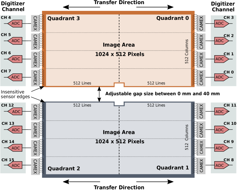
Two vacuum motion stages allow separation of the sensor halves in vertical () direction with a precision of , i.e. perpendicular to the FEL beam. The resulting gap between the two halves of the pnCCD sensor is up to wide, allowing the user to enlarge the detection plane in order to cover a larger range. Passage of the primary FEL beam is enabled by a laser cut, large, rectangular hole as illustrated in Fig. 2. The slit and the hole can be completely closed, as the two sensor planes can be staggered leaving a gap of between the sensor planes in beam direction, with the top half covering the lower half. When the slit is completely closed, a insensitive area remains between the lowest pixel column of the top detector half and the uppermost pixel column of the bottom half, whereby no part of the sensitive sensor area is blocked.
The significantly reduced thermally generated dark-current of the latest generation pnCCDs in comparison to earlier versions [Holl:2006a], allows operating the pnCCD sensors at temperatures up to while achieving an electronic noise level of rms in high gain and about rms in low gain. To achieve the best imaging and spectroscopic performance, temperature stability of the sensor better than is required.
The thermal power budget of the sensor plane is dominated by the thermal dissipation power of the Application Specific Integrated Circuit (ASIC) chips mounted next to the pnCCD sensors on the sensor hybrid board (see Section 3, Fig. 3 and Fig. 4). During readout of the pnCCD, each of the ASICs contributes with to the total power budget of . In order to reduce the power dissipation to a minimum, the ASICs are switched to stand-by when not needed for signal processing, e.g. during the integration phase of the CCD’s image taking cycle.
The detector’s active cooling system is optimized to the above mentioned requirements. It is seamlessly integrated into the camera and the motion system. Rigid high-conductivity copper connections transfer the heat from the Al-Si alloy sensor frame to the rear side of the sensor plane. Subsequently, four flexible copper braids transmit the dissipated thermal power to the in-vacuum cold fingers of two Polycold® Compact Coolers (PCC). In the configuration used for this application, the PCCs provide a maximum cooling power of . With this design, the sensor temperature is stable to better than . This temperature tolerance is sufficient in significantly minimizing the detector’s dark current and noise, as needed in photon-sensitive X-ray imaging. The time required to cool the pnCCDs in vacuum from room temperature to the nominal operating temperature of , and to reach stable thermal operating conditions is about . Temperature stability over a time scale of days within the above mentioned requirement has been demonstrated with this design.
During detector operation, the temperature of the pnCCD sensor is continuously monitored via four platinum resistance thermometers (type PT 1000) mounted on the cold fingers and the copper block attached to the pnCCD modules. The temperature readings, amongst other slow control values, are logged by the Karabo control system of the European XFEL [hauf:2019a]. The pnCCD calibration pipeline can use these temperature values as reference for data correction and processing (see Sec. 3).
2.2 pnCCD Sensor and Signal Processing
The pnCCD sensor plane has a sensitive area of and consists of two monolithic chips (sensor halves) as schematically shown in Fig. 4. Both are identically designed, back-illuminated pnCCDs. Each has pixels and a fully depleted, thick sensitive volume. The pixel size of allows for sub-pixel position resolution of better than (at normal incidence) in the single photon detection regime when charge centroiding techniques are applied [Ihle:2017a]. The two halves are operated and read out independently in a split-frame mode (see Fig. 4). Further performance parameters of the sensor and readout electronics are summarized in Table 1.
During the readout process, the signal charges generated by X-ray photons are transferred line by line along the pnCCD transfer columns. Each column is terminated by a charge collecting anode connected to an integrated n-channel junction gate field-effect transistor (JFET). This on-chip amplifier is operated in source follower mode and bonded to one input channel of the CMOS Amplifier and MultiplEX (CAMEX) ASIC [Buttler:88a, Herrmann:2008a]. This column-parallel signal amplification concept allows for high frame rates in combination with low noise performance.
In total CAMEX ASICs with inputs each are required for handling the signal of the JFET source follower outputs of each pnCCD chip. For further signal processing, the CAMEX provides two-stage amplification, filtering, noise bandwidth limitation and 8-fold Correlated Double Sampling (CDS). The multiple baseline and signal sampling enabled by the CDS increases the signal to noise ratio proportional to , where is the number of sampling points. Through a digital control register it is possible to adjust the gain of the pre-amplifiers to the experimental conditions. Apart from the highest gain , gain values of and can be configured before data taking. Finally the signal is stored in a sample and hold (S&H) stage before all parallel channels are multiplexed in analog output channel per CAMEX.
After serialization by the CAMEX, the analog signal is transferred to and digitized by two SIS8300 digitizer boards providing 10 ADC channels with 16 bit resolution each. The EuXFEL uses these boards as a facility-wide standard for high speed digitizer applications. The boards sample the signal with a frequency between and per channel. Application specific readout, data formatting, data reduction and processing algorithms can be implemented on a Virtex V Field Programmable Gate Array (FPGA) available on the SIS8300 board [Struck:2020a]. Each board in addition reads the pixel clock signal provided by the timing sequencer of the pnCCD for synchronization. The digitizer FPGA firmware is configured to sample 800 kSamples per CAMEX and image, as determined by the 10 Hz train trigger, which corresponds to 1 or 2 samples per pixel and readout cycle. The CAMEX is typically operated at , enabling image rates up to frames per second.
Figure 4 shows the geometric arrangement of the sensor plane, the signal transfer direction, and illustrates how the ASIC chips are arranged on the right and left side of the sensor chips. The designation of the output channels of the ADCs and detector quadrants is the same as the one used in the meta data of the Karabo online data stream and the HDF5 [hdf5:2020a] raw/calibrated data files.
Visible and infrared background light, e.g. from a pump-laser, can significantly deteriorate the signal to noise ratio of an experiment, especially when aiming at photon energies and small scattering signals. A blocking filter for visible and IR light is therefore crucial for maintaining a high signal to noise ratio in the presence of background signal sources. In general two technological solutions exist to mitigate this problem, either by using a thin and coated foil, mounted in front of the sensor plane, or by a filter deposited on the entrance window of the sensor. Appropriate foils, having a thickness of a few hundred nanometers, are very fragile and require a support structure, that may additionally scatter photons as undesired background signal.
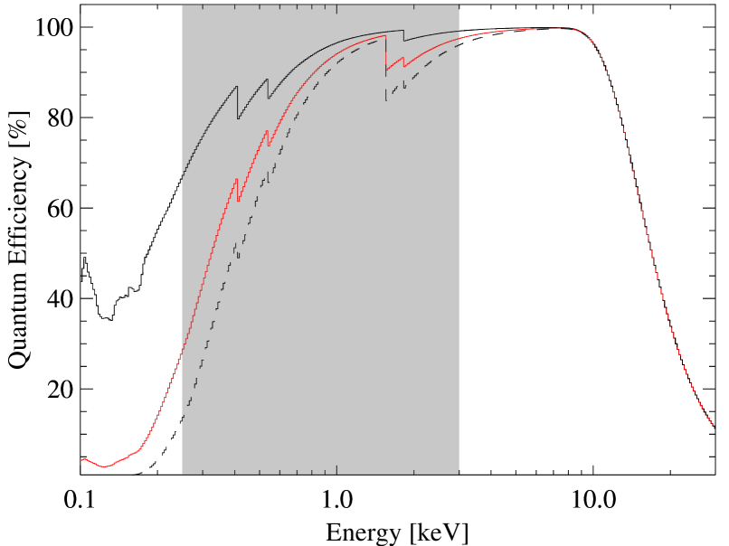
With a light blocking filter directly deposited on the entrance window of the sensor, we can circumvent these disadvantages. The design of such a filter requires a careful trade-off between attenuation of visible light and the desired X-ray quantum efficiency. For this detector, we have chosen an in total thin blocking filter, consisting of layers of aluminium, and directly deposited on the -doped silicon sensor backside. During a major upgrade planned in the second half of 2020, we will implement a new sensor module with an improved sensitivity for low energy photons, enabled by the implementation of a thinner aluminum entrance window with a thickness of 60 nm. The combination of the three layers efficiently attenuates photons with energies between and by at least a factor of using a and with a thick aluminium layer as shown in Fig. 5. A further benefit of this kind of ultra-thin entrance window is its homogeneous response to low energy photons, resulting in good energy resolution and high quantum efficiency of at least in the energy range between and (see Fig. 6).
2.3 pnCCD Read Out Timing and Synchronization to the XFEL Pulse Pattern
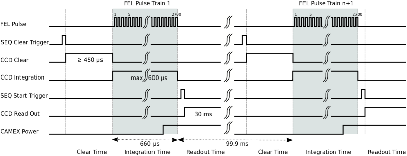
The EuXFEL machine delivers up to spatially coherent X-ray pulses per second in a unique time structure. Ten times per second, a train of equidistantly separated X-ray pulses arrives at the sample interaction point in the NQS sample chamber as shown in the topmost line of Fig. 7. Each pulse train can contain between and up to X-ray pulses with a minimum inter pulse separation of . This corresponds to a maximum pulse repetition frequency of .
The synchronization of the detector is accomplished through the EuXFEL timing system [Gessler:2020a], which provides triggers to the sequencer of the pnCCD. Since the sequencer uses an internal clock, the SIS8300 ADC is synchronized to the sequencer to ensure phase aligned readout of the detector signals. In this way, the detector front-end is correctly aligned with the timing of the machine.
Since the pnCCD is continuously biased, the sensor bulk is sensitive to visible, IR and X-ray photons at any time of the integration and readout cycle. As a consequence photons being absorbed in the depleted sensor bulk between two consecutive readout cycles would create a potential background signal which does not originate in an interaction of the FEL beam with the sample. Therefore, the pnCCD sensor is cleared of charge before the arrival of the first X-ray FEL pulses by quickly shifting residual charges to the readout anode and discarding the charge signal.
This long clear process is followed by the signal integration period (see Fig. 7) with a duration chosen according to scientific requirements. Its minimum duration is , with an upper limit given, e.g. by the desired time resolution. A typical value is which is sufficient to record all signals produced by the X-ray pulses within one pulse train. The final signal readout, amplification, filtering and digitization take additional . The readout sequence is synchronized to the EuXFEL bunch pattern through the SEQUENCER_CLEAR_TRIGGER and SEQUENCER_START_TRIGGER signals provided by the CC system, respectively. Both trigger signals are sent to Karabo.
In general the pnCCD’s sequencer generating the readout sequence and control signals for the CAMEX and the CCD can be programmed in a very flexible way, such that the CCD’s readout and signal processing sequence can be adjusted to and optimized for specific experimental requirements. Nevertheless, for most scenarios, changing the readout sequence requires a recalibration of the detector for achieving the ideal performance as shown in Section 4.
3 Data Processing, Correction and Calibration
The pnCCD online data processing and correction is integrated into Karabo as configurable pipelines build of different components, referred to as devices. They provide specific signal correction, data processing, data managing and data handling functionality.
Both the digitized analog and pixel clock signals are read out from the SIS8300 boards by a C++ software integrated as a device into the control system. A second device samples the pixel signal synchronized to the pixel clock (see Fig. 7). Furthermore, it reformats the one-dimensional digitizer data stream into sub-images with pixels each (one per CAMEX output channel) and assembles them into the full Megapixel image. Since the two digitizer cards are read out independently, the two input data streams are synchronized by the timing information provided as train IDs in the trigger process. The assembled image data is then output as a 2D array with 16 bits resolution per pixel via a network link to the data acquisition system. Finally, the full 2D images are stored into HDF5 files, and provided as a data stream to online visualization and processing. All software discussed is running on a CPU card hosted in the same TCA crate with the SIS8300 boards, communication being done via PCI Express.
As offline data processing is not required for rapid feedback and direct interfacing to detector hardware, it is conceptually implemented as a stand-alone processing pipeline. It is aimed at providing the highest possible data quality, i.e. hardware limited calibrated images and spectroscopic data. This pipeline is implemented in Python and distributed through the pyDetLib library. On the other hand, online processing and visualization is required for rapid feedback to the detector operators and users and, therefore, another set of processing pipeline.
Calibration and correction parameters and their metadata are managed by the XFEL calibration data base, stored in HDF5 files and archived on tape. Parameters used for data correction are selected by evaluating detector settings and conditions under which the data for correction and calibration have been acquired. The correction parameter set closest in time to the measured scientific data to be corrected and best matching the detector settings is finally used. The parameter sets are divided into two different classes, one set is provided by the facility and the other set is acquired during the user beam time. The latter parameter set might depend and change according to experiment conditions, while the first parameter set does not change significantly on the long term (i.e. on a time scale of weeks to months).
For the pnCCD, the following calibration and correction parameters are available for each gain setting through the XFEL calibration data base and, if necessary, may be updated before a user’s beam time [Kuster:2014a]:
-
•
The gain vectors and for conversion of analog digital units (ADU) to photon numbers,
-
•
a vector characterizing the relative variation of the amplification between the 128 different parallel CAMEX readout channels for all 16 ASICs and
-
•
the charge transfer inefficiency (CTI) for each sensor column quantifying the charge loss during charge transfer from the photon interaction point to the readout anode.
The following parameters are experiment specific and are determined from data acquired during an experiment:
-
•
The offset map providing the per pixel offset,
-
•
the noise map providing the per pixel rms noise , and the corresponding bad pixel map .
In the following sections we describe the data processing steps applied to pnCCD data, as implemented in the online and offline data processing pipelines in more detail. The information provided reflects the status as of December 2019, corresponding to the following software releases: Karabo V 2.4.2, pnCCD calibration pipeline pycalibration V 2.0, calPy V 1.9.1-2.4.1, calibration data base cal_db_interactive V 1.0, the fasterADC V 2.6.1-2.4.0 and cppPnCCDFormatter V 1.1.1-2.4.1 devices.
3.1 Online Processing
Before scientific data are processed online, a data set for offset and noise calculation is typically acquired before each experimental run. The offset and noise maps are subsequently calculated per pixel in one single pass using the numerical algorithm of \citeasnounWelford:1962a. Welford’s algorithm is based on updating the sum of squares of differences
| (1) |
for estimating the mean of a population of values. The mean for the current follows for from
| (2) |
and the variance from
| (3) |
were is the mean calculated from the first samples. We calculate the mean signal value of each pixel according to equation 2 and assign it to the offset map as value , where and indicate the column and line numbers of the sensor, the signal charge measured at pixel position and the number of image frames used for the calculation. In a similar fashion, the noise map entry is calculated from the per pixel variance as . By default, the sample size for mean, variance and standard deviation calculation for each pixel is set to images. The resulting offset and noise maps are finally injected into the calibration data base. Either this offset map is subtracted from the scientific data during online processing or an offset map matching the experimental and detector conditions closest is used.
In the latter case, the following detector parameters are taken into consideration for selecting the best matching offset map: CCD temperature, CCD bias voltage, integration time and the chosen CAMEX gain settings. The result of the correction is stored as pixel arrays in the corrected data files. During this step, the scientific data are up-converted from 16 bit unsigned integer values to 32 bit float values.
Subsequently, a line-by-line common mode correction reduces baseline variations of the analog pixel signal. The number of pixels in each line taken into account for the common mode calculation is configurable to the number of pixels per ASIC (i.e. pixels), the dimension of a sensor quadrant ( pixels) or sensor half ( pixels). The common mode value is then calculated from the sorted vector as
| (4) |
and subsequently subtracted from the signal in each pixel of one line.
For the pnCCD it has been found that evaluating the common mode as a thresholded median for each quadrant gives a good trade-off between accuracy and stability against event-rich images. In that case, only pixels in one line which are carrying a signal below the threshold are taken into consideration for the calculation of the line’s median value.
Further and higher order data treatment like charge sharing, charge transfer efficiency corrections and correction of the variations of the relative amplification of the 128 CAMEX channels are not taken into account during online processing.
The online corrected images are then passed on to the Karabo Graphical User Interface (Karabo GUI) for visualization or to the Karabo-Bridge for interfacing to user-provided processing using the ZMQ protocol [Fangohr:2018a].
3.2 Offline Processing
Offline processing is performed on recorded data files. It is either automatically triggered when users migrate data to be archived and made available on the Maxwell HPC cluster [Maxwell:2020a], or explicitly using the Metadata Catalogue web interface. Offline processing retrieves necessary calibration and correction parameters from the calibration database in a similar way as the online processing pipeline.
By default, the offset correction is always performed using the same offset maps as the ones used by the online processing pipeline. Furthermore a line-by-line common mode correction using by default the same feature size as for online processing is applied. The result of this correction is output into the pixel_cm array in the corrected data files. For correcting the data presented in Section 4, a median value which is calculated from the outermost pixels in each line gives the best results with respect to flat field baseline homogeneity. Attention should be paid to the fact that the common mode correction is prone to be biased or can even completely fail for very event-rich images. Consequently, the methodology for common mode correction should be carefully chosen during offline processing.
Noisy pixels, pixels providing no signal (e.g. the area of the central hole) or a non-physical signal and events produced by cosmic rays are excluded from the analysis and marked in the bad pixel map in the calibration data base. Pixels marked as bad are excluded from further treatment during the offline processing.
Split event correction, also called charge sharing correction or charge clustering, is always performed. It classifies clustered signals of discrete photon events by the number of adjacent pixels the charge is detected in. The signal in each pixel is probed against two thresholds prior to event classification: a primary event threshold to identify the pixel carrying the majority charge of the total signal of a photon event and a secondary (lower) threshold for identifying neighboring pixels as having registered a signal above the noise floor. Both thresholds are given in units of , where is the pixels specific rms noise given by the noise map. The algorithm then searches for valid charge clusters that can originate in a photon interaction and sums all charges above noise into an event reconstructed primary pixel carrying the majority charge. Clusters that cannot be attributed to a single photon event are identified via a special pattern index. Their charge is not summed up. The result of this correction is stored into the pixel_classified array. Additionally, a patterns_classified array is generated, which encodes event multiplicity and orientation.
If relative gain correction is activated, the aforementioned pixel arrays will be stored corrected for the relative difference of the amplification of the amplifiers of the 128 channels of each CAMEX.
The Charge Transfer Inefficiency (CTI) of the present generation pnCCDs is better than , leaving a potential signal shift by after 512 charge transfer steps. The CAMEX channel to channel amplification variation is less than of the detected signal charge. Both corrections are of minor importance for imaging applications and are therefore presently neglected during default offline image correction, but can be enabled during manual data reprocessing to achieve the best possible spectroscopic performance.
Conversion from analog digital units (ADU) to photon numbers is performed by means of a gain calibration vector, one for each possible gain configuration . This conversion is performed for the three output arrays: pixels, pixels_cm and pixels_classified.
For an in depth description of data correction and treatment and its implementation of the XFEL pyDetLib, we refer to the corresponding user manuals [pyDetLib:2020a]. The data presented in the following sections have been treated offline in the same way as described in the previous section.
4 Detector Performance
After installation of the detector at the NQS station, we commissioned the pnCCD detector and characterized its performance before the first user beamtime, which took place shortly thereafter during EuXFEL’s user runs in the first and second half of 2019 (run period 03 and 04 at EuXFEL). We investigated the detector’s noise behavior and photon response under nominal operating conditions, i.e. at stable sensor temperature and optimized detector operating parameters, like bias voltage settings, CAMEX configuration and readout sequence of the CCD. The performance figures provided in this section refer to the performance as measured at the SQS experimental environment.
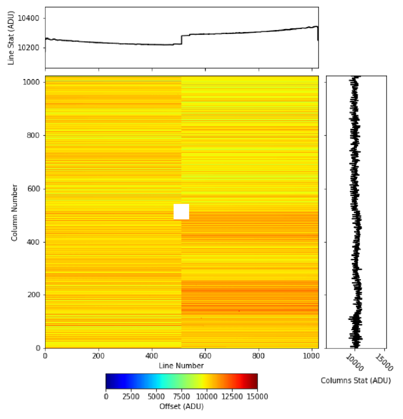
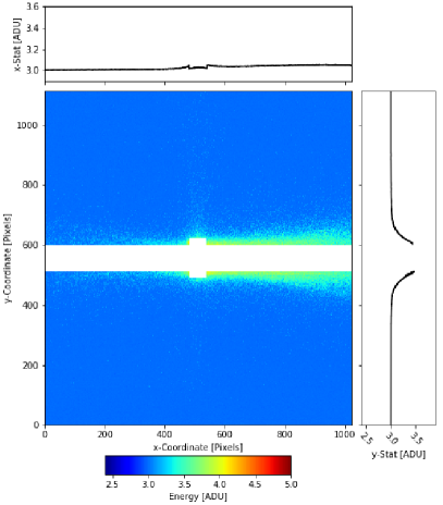
Figure 8 shows an exemplary offset map calculated from 400 individual images acquired with gain during the user run period 03. The dark distribution shows the typical regular stripe structure along the sensor columns expected from a CCD with column parallel readout. This structure can be attributed to channel-to-channel baseline variations of the 128 CAMEX input channels.
The spatial distribution of the corresponding rms noise is shown in Fig. 9 measured with gain (left image) and (right image). The features of the dark and noise maps in Fig. 9 can be regarded as exemplary for the operating conditions and parameter settings used with the pnCCD detector during the EuXFEL’s user beam time.
As mean dark signal calculated across the whole chip we find . The corresponding per pixel noise of , translates into an equivalent noise charge (ENC) of , when taking the ADU to photon energy conversion factor of (gain ) into consideration. The EuXFEL pnCCD detector is thus capable of discriminating single photons with an energy of and from the noise floor with a significance of and , respectively.
An example of the detector’s imaging performance is demonstrated by Fig. 10. This diffraction pattern was acquired during the first user beam time using the pnCCD installed at the NQS chamber in June 2019 [Tanyag:2020a]. The diffraction image was obtained from a micron-sized superfluid helium droplets containing millions of acetonitrile molecules. The droplets were hit by one single FEL pulse focused to a diameter of about , with a photon energy of ,
The detector was configured to gain , in order to avoid saturation of the pixels close to the central imaging area. The area of the central hole is excluded from the analysis. Further data treatment includes subtracting the experimental background captured by the imaging frame before the helium diffraction pattern (bottom left picture of Fig. 10).
The influence of the data corrections applied during offline analysis is illustrated by comparing the bottom left picture of Fig. 10 with the fully corrected diffraction pattern on the top. The bottom left picture shows the same diffraction pattern as provided by the front end electronics at the output of the ADC. Apart from normalization of the mean baseline to the baseline of the corrected image, no further data corrections were applied to this image. The uncorrected image shows all features of the detector’s dark signal, common mode effects, experiment background and the diffraction signal on top. The horizontal stripes result from variations in the baseline and gain for each CAMEX readout channel. Furthermore, a non-zero signal is apparent from the area of the central hole. This is the consequence of the way the pnCCD sensor is read out. Since the readout sequence always considers pixels to be processed by the CAMEX, the CAMEX provides an output signal to the ADC even for the area corresponding to the central hole.
5 Conclusions and Outlook
The EuXFEL 1-Megapixel pnCCD detector enables experimental techniques like coherent diffraction imaging at the SQS instrument with single photon sensitivity on a and significance level at the lowest photon energies provided by the FEL, i.e. in the future and presently .
The detector is installed at the EuXFEL’s SQS instrument and has successfully been integrated into the NQS endstation, tested and subsequently commissioned in May 2019. The fully equipped NQS endstation is available for the European XFEL’s user community since June 2019 for investigations of the interaction of intense FEL pulses with clusters, nano-particles and small bio-molecules exploiting coherent diffraction imaging techniques. Since then, the pnCCD detector and the NQS endstation have already been successfully used by the scientific community for several experiments during user runs in the first and second half of 2019 at EuXFEL.
The detector system is integrated into the EuXFEL’s facility-wide control system Karabo, enabling the EuXFEL standardized control, online/offline data processing, on the fly data correction and data calibration. During the commissioning phase and first user experiments, stable operation with a noise level below ENC was demonstrated (see Tab. 1).
Further improvements of the performance of the detector are expected after the present sensor module has been replaced by a further optimized one. This major upgrade is planned for the second half of 2020. The new sensor module will provide an improved sensitivity for low energy photons, enabled by the implementation of a thinner aluminum entrance window with a thickness of in comparison to of the present one. This results in a factor of higher quantum efficiency at . An extensive multi-energy calibration campaign of the pnCCD will follow this upgrade, with the main goals of enabling best possible sensitivity and the spectroscopic capabilities of the pnCCD with Fano-Noise-limited energy resolution.
Further information about the SQS instrument, the NQS station, data processing/correction, and the pnCCD detector can be found on the EuXFEL’s webpages [SQS:2020a].
Acknowledgement We acknowledge European XFEL in Schenefeld, Germany, for provision of X-ray free-electron laser beamtime at the SQS instrument and would like to thank the staff for their assistance. The work presented in this publication was funded by EuXFEL. D.R., R.T., and A.U. acknowledge funding from the Bundesministerium für Bildung und Forschung via grant No. 05K16KT3, within the BMBF Forschungsschwerpunkt Freie-Elektronen-Laser FSP-302 and from the Leibniz-Gemeinschaft via grant No. SAW/2017/MBI4. We would like to thank specifically the following EuXFEL groups for their fruitful collaboration, vital contribution to this work and their continuous effort in supporting this project: Control devices were developed by the Control and Analysis Software (CAS) group led by Sandor Brockhauser, the motor control hardware, timing system and PLC systems were contributed by the Electronic & Electrical Engineering (EEE) group led by Patrick Gessler, data acquisition and storage is provided by the Information Technology and Data Management (ITDM) group led by Krzystof Wrona.
References
-
[1]
\harvarditem[Allahgholi et al.]Allahgholi, Becker, Delfs, Dinapoli,
Goettlicher, Greiffenberg, Henrich, Hirsemann, Kuhn, Klanner, Klyuev,
Krueger, Lange, Laurus, Marras, Mezza, Mozzanica, Niemann, Poehlsen,
Schwandt, Sheviakov, Shi, Smoljanin, Steffen, Sztuk-Dambietz, Trunk, Xia,
Zeribi, Zhang, Zimmer, Schmitt \harvardand Graafsma2019Allahgholi:2019a
Allahgholi, A., Becker, J., Delfs, A., Dinapoli, R., Goettlicher, P.,
Greiffenberg, D., Henrich, B., Hirsemann, H., Kuhn, M., Klanner, R., Klyuev,
A., Krueger, H., Lange, S., Laurus, T., Marras, A., Mezza, D., Mozzanica, A.,
Niemann, M., Poehlsen, J., Schwandt, J., Sheviakov, I., Shi, X., Smoljanin,
S., Steffen, L., Sztuk-Dambietz, J., Trunk, U., Xia, Q., Zeribi, M., Zhang,
J., Zimmer, M., Schmitt, B. \harvardand Graafsma, H. \harvardyearleft2019\harvardyearright.
Journal of Synchrotron Radiation, \volbf26(1), 74–82.
\harvardurlhttps://doi.org/10.1107/S1600577518016077 - [2] \harvarditem[Altarelli et al.]Altarelli, Reinhard \harvardand Chergui2007Altarelli:2006a Altarelli, M., Reinhard, B. \harvardand Chergui, M., \harvardyearleft2007\harvardyearright. The European X-Ray Free-Electron Laser. Technical Design Report DESY 2006-097.
- [3] \harvarditem[Buttler et al.]Buttler, Lutz, Bergmann, Dietl, Hauff, Holl \harvardand Manfredi1988Buttler:88a Buttler, W., Lutz, G., Bergmann, H., Dietl, H., Hauff, D., Holl, P. \harvardand Manfredi, P. F. \harvardyearleft1988\harvardyearright. Nuclear Instruments and Methods in Physics Research A, \volbf273(2-3), 778–783.
- [4] \harvarditem[Decking et al.]Decking, Abeghyan, Abramian, Abramsky, Aguirre, Albrecht, lou, Altarelli, Altmann, Amyan, Anashin, Apostolov, Appel, Auguste, Ayvazyan, Baark, Babies, Baboi, Bak \harvardand Zybin2020Decking:2020a Decking, W., Abeghyan, S., Abramian, P., Abramsky, A., Aguirre, A., Albrecht, C., lou, P., Altarelli, M., Altmann, P., Amyan, K., Anashin, V., Apostolov, E., Appel, K., Auguste, D., Ayvazyan, V., Baark, S., Babies, F., Baboi, N., Bak, P. \harvardand Zybin, D. \harvardyearleft2020\harvardyearright. Nature Photonics, \volbf14, 391–397.
-
[5]
\harvarditemDESY2020Maxwell:2020a
DESY, \harvardyearleft2020\harvardyearright.
Maxwell HPC Resources at DESY Hamburg.
DESY Webpage.
Status July 2020.
\harvardurlhttps://confluence.desy.de/display/IS/Maxwell - [6] \harvarditem[Doering et al.]Doering, Andresen, Contarato, Denes, Josephand P. McVittie, Walder \harvardand Weizeorick2012Doering:2012a Doering, D., Andresen, N., Contarato, D., Denes, P., Josephand P. McVittie, J., Walder, J. \harvardand Weizeorick, J. \harvardyearleft2012\harvardyearright. In 2012 IEEE Nuclear Science Symposium and Medical Imaging Conference Record (NSS/MIC), pp. 527–529.
- [7] \harvarditem[Emma et al.]Emma, Akre, Arthur, Bionta, Bostedt, Bozek, Brachmann, Bucksbaum, Coffee, Decker, Ding, Dowell, Edstrom, Fisher, Frisch, Gilevich, Hastings, Hays, Hering, Huang, Iverson, Loos, Messerschmidt, Miahnahri, Moeller, Nuhn, Pile, Ratner, Rzepiela, Schultz, Smith, Stefan, Tompkins, Turner, Welch, White, Wu, Yocky \harvardand Galayda2010Emma:2010a Emma, P., Akre, R., Arthur, J., Bionta, R., Bostedt, C., Bozek, J., Brachmann, A., Bucksbaum, P., Coffee, R., Decker, F. J., Ding, Y., Dowell, D., Edstrom, S., Fisher, A., Frisch, J., Gilevich, S., Hastings, J., Hays, G., Hering, P., Huang, Z., Iverson, R., Loos, H., Messerschmidt, M., Miahnahri, A., Moeller, S., Nuhn, H. D., Pile, G., Ratner, D., Rzepiela, J., Schultz, D., Smith, T., Stefan, P., Tompkins, H., Turner, J., Welch, J., White, W., Wu, J., Yocky, G. \harvardand Galayda, J. \harvardyearleft2010\harvardyearright. Nature Photonics, \volbf4(9), 641–647.
-
[8]
\harvarditemEppink \harvardand Parker1997Eppink:1997a
Eppink, A. T. J. B. \harvardand Parker, D. H. \harvardyearleft1997\harvardyearright.
Review of Scientific Instruments, \volbf68(9), 3477–3484.
\harvardurlhttps://doi.org/10.1063/1.1148310 -
[9]
\harvarditemEuXFEL2020pyDetLib:2020a
EuXFEL, \harvardyearleft2020\harvardyearright.
XFEL Detector Tools’ Documentation.
European XFEL GmbH.
Revision 2f1352a2.
\harvardurlhttps://in.xfel.eu/readthedocs/docs/pydetlib/en/latest/index.html -
[10]
\harvarditem[Fangohr et al.]Fangohr, Beg, Bondar, Boukhelef,
Brockhauser, Danilevski, Ehsan, Esenov, Flucke, Giovanetti, Göries, Hauf,
Heisen, Hicklin, Khalkulin, Klimovskaia, Kuster, Lang, Maia, Mekinda,
Michelat, Parenti, Previtali, Santos, Silenzi, Sztuk-Dambietz, Szuba,
Teichmann, Weger, Wiggins, Wrona, Xu, Aplin, Barty, Kuhn, Mariani
\harvardand Kluyver2018Fangohr:2018a
Fangohr, H., Beg, M., Bondar, V., Boukhelef, D., Brockhauser, S., Danilevski,
C., Ehsan, W., Esenov, S. G., Flucke, G., Giovanetti, G., Göries, D., Hauf,
S., Heisen, B. C., Hicklin, D. G., Khalkulin, D., Klimovskaia, A., Kuster,
M., Lang, P. M., Maia, L., Mekinda, L., Michelat, T., Parenti, A., Previtali,
G., Santos, H., Silenzi, A., Sztuk-Dambietz, J., Szuba, J., Teichmann, M.,
Weger, K., Wiggins, J., Wrona, K., Xu, C., Aplin, S., Barty, A., Kuhn, M.,
Mariani, V. \harvardand Kluyver, T. \harvardyearleft2018\harvardyearright.
In Proc. of International Conference on Accelerator and Large
Experimental Control Systems (ICALEPCS’17), pp. 245–252. Geneva,
Switzerland: JACoW.
\harvardurlhttp://jacow.org/icalepcs2017/papers/tucpa01.pdf - [11] \harvarditemGatner2010Ganter:2010a Gatner, R., \harvardyearleft2010\harvardyearright. SwissFEL - Conceptual Design Report. Paul Scherrer Institut PSI-10-04.
-
[12]
\harvarditem[Gessler et al.]Gessler, Ali, Ballak, Bamaga, Baranasic,
Bieler, Coppola, Dornack, Eilers, Emes, Fernndes, Fobian, Huynh,
Jardon Bueno, Meyer, Oshtuk, Parlicki, Reifschläger, Sayar \harvardand Sotoudi Namin2020Gessler:2020a
Gessler, P., Ali, H., Ballak, K.-E., Bamaga, H., Baranasic, B., Bieler, O.,
Coppola, N., Dornack, K., Eilers, J., Emes, D., Fernndes, B., Fobian,
M. Freyermuth, T., Huynh, S. T., Jardon Bueno, N., Meyer, M., Oshtuk, O.,
Parlicki, P., Reifschläger, J., Sayar, S. \harvardand Sotoudi Namin,
H. \harvardyearleft2020\harvardyearright.
In Proc. of the 17th International Conference on Accelerator
and Large Experimental Physics Control Systems (ICALEPCS’19), New York, NY,
USA, p. 7. Geneva, Switzerland: JACoW.
In Press.
\harvardurlhttp://icalepcs2019.vrws.de/papers/thapp05.pdf -
[13]
\harvarditem[Graafsma et al.]Graafsma, Becker \harvardand Gruner2020Graafsma:2020a
Graafsma, H., Becker, J. \harvardand Gruner, S. M. \harvardyearleft2020\harvardyearright.
Integrating Hybrid Area Detectors for Storage Ring and
Free-Electron Laser Applications, pp. 1225–1255.
Springer International Publishing.
\harvardurlhttps://doi.org/10.1007/978-3-030-23201-6_37 - [14] \harvarditem[Hart et al.]Hart, Angelsen, Burge, Coughlan, Halsall, Koch, Kuster, Nicholls, Prydderch, Seller, Thomas, Blue, Joy, O’shea \harvardand Wing2012Hart:2012 Hart, M., Angelsen, C., Burge, S., Coughlan, J., Halsall, R., Koch, A., Kuster, M., Nicholls, T., Prydderch, M., Seller, P., Thomas, S., Blue, A., Joy, A., O’shea, V. \harvardand Wing, M. \harvardyearleft2012\harvardyearright. In 2012 IEEE Nuclear Science Symposium and Medical Imaging Conference Record (NSS/MIC), pp. 534–537.
-
[15]
\harvarditemHatsui \harvardand Graafsma2015Hatsui:2015a
Hatsui, T. \harvardand Graafsma, H. \harvardyearleft2015\harvardyearright.
IUCrJ, \volbf2(3), 371–383.
\harvardurlhttps://doi.org/10.1107/S205225251500010X -
[16]
\harvarditem[Hauf et al.]Hauf, Heisen, Aplin, Beg, Bergemann, Bondar,
Boukhelef, Danilevsky, Ehsan, Essenov, Fabbri, Flucke, Fulla Marsa,
Göries, Giovanetti, Hickin, Jarosiewicz, Kamil, Khakhulin, Klimovskaia,
Kluyver, Kirienko, Kuhn, Maia, Mamchyk, Mariani, Mekinda, Michelat,
Münnich, Padee, Parenti, Santos, Silenzi, Teichmann, Weger, Wiggins,
Wrona, Xu, Youngman, Zhu, Fangohr \harvardand Brockhauser2019hauf:2019a
Hauf, S., Heisen, B., Aplin, S., Beg, M., Bergemann, M., Bondar, V., Boukhelef,
D., Danilevsky, C., Ehsan, W., Essenov, S., Fabbri, R., Flucke, G.,
Fulla Marsa, D., Göries, D., Giovanetti, G., Hickin, D., Jarosiewicz,
T., Kamil, E., Khakhulin, D., Klimovskaia, A., Kluyver, T., Kirienko, Y.,
Kuhn, M., Maia, L., Mamchyk, D., Mariani, V., Mekinda, L., Michelat, T.,
Münnich, A., Padee, A., Parenti, A., Santos, H., Silenzi, A.,
Teichmann, M., Weger, K., Wiggins, J., Wrona, K., Xu, C., Youngman, C., Zhu,
J., Fangohr, H. \harvardand Brockhauser, S. \harvardyearleft2019\harvardyearright.
Journal of Synchrotron Radiation, \volbf26(5), 1448–1461.
\harvardurlhttps://doi.org/10.1107/S1600577519006696 -
[17]
\harvarditem[Herrmann et al.]Herrmann, Buttler, Hartmann, Meidinger,
Porro \harvardand Strüder2008Herrmann:2008a
Herrmann, S., Buttler, W., Hartmann, R., Meidinger, N., Porro, M. \harvardand Strüder, L. \harvardyearleft2008\harvardyearright.
IEEE Nuclear Science Symposium and Medical Imaging conference
(2008 NSS/MIC), pp. 2952–2957.
\harvardurlhttps://ieeexplore.ieee.org/document/4774983 - [18] \harvarditem[Holl et al.]Holl, Andritschke, Eckhardt, Hartmann, Koitsch, Lutz, Meidinger, Richter, Schaller, Soltau, Strüder \harvardand Valceanu2006Holl:2006a Holl, P., Andritschke, R., Eckhardt, R., Hartmann, R., Koitsch, C., Lutz, G., Meidinger, N., Richter, R., Schaller, G., Soltau, H., Strüder, L. \harvardand Valceanu, G. \harvardyearleft2006\harvardyearright. vol. 3, pp. 1589–1594.
-
[19]
\harvarditem[Ihle et al.]Ihle, Holl, Kalok, Hartmann, Ryll,
Steigenhöfer \harvardand Strüder2017Ihle:2017a
Ihle, S., Holl, P., Kalok, D., Hartmann, R., Ryll, H., Steigenhöfer, D.
\harvardand Strüder, L. \harvardyearleft2017\harvardyearright.
Journal of Instrumentation, \volbf12(02), P02005–P02005.
\harvardurlhttps://iopscience.iop.org/article/10.1088/1748-0221/12/02/P02005/pdf - [20] \harvarditem[Ishikawa et al.]Ishikawa, Aoyagi, Asaka, Asano, Azumi, Bizen, Ego, Fukami, Fukui, Furukawa, Goto, Hanaki, Hara, Hasegawa, Hatsui, Higashiya, Hirono, Hosoda, Ishii, Inagaki, Inubushi, Itoga, Joti, Kago, Kameshima, Kimura, Kirihara, Kiyomichi, Kobayashi, Kondo, Kudo, Maesaka, Maréchal, Masuda, Matsubara, Matsumoto, Matsushita, Matsui, Nagasono, Nariyama, Ohashi, Ohata, Ohshima, Ono, Otake, Saji, Sakurai, Sato, Sawada, Seike, Shirasawa, Sugimoto, Suzuki, Takahashi, Takebe, Takeshita, Tamasaku, Tanaka, Tanaka, Tanaka, Togashi, Togawa, Tokuhisa, Tomizawa, Tono, Wu, Yabashi, Yamaga, Yamashita, Yanagida, Zhang, Shintake, Kitamura \harvardand Kumagai2012Ishikawa:2012a Ishikawa, T., Aoyagi, H., Asaka, T., Asano, Y., Azumi, N., Bizen, T., Ego, H., Fukami, K., Fukui, T., Furukawa, Y., Goto, S., Hanaki, H., Hara, T., Hasegawa, T., Hatsui, T., Higashiya, A., Hirono, T., Hosoda, N., Ishii, M., Inagaki, T., Inubushi, Y., Itoga, T., Joti, Y., Kago, M., Kameshima, T., Kimura, H., Kirihara, Y., Kiyomichi, A., Kobayashi, T., Kondo, C., Kudo, T., Maesaka, H., Maréchal, X. M., Masuda, T., Matsubara, S., Matsumoto, T., Matsushita, T., Matsui, S., Nagasono, M., Nariyama, N., Ohashi, H., Ohata, T., Ohshima, T., Ono, S., Otake, Y., Saji, C., Sakurai, T., Sato, T., Sawada, K., Seike, T., Shirasawa, K., Sugimoto, T., Suzuki, S., Takahashi, S., Takebe, H., Takeshita, K., Tamasaku, K., Tanaka, H., Tanaka, R., Tanaka, T., Togashi, T., Togawa, K., Tokuhisa, A., Tomizawa, H., Tono, K., Wu, S., Yabashi, M., Yamaga, M., Yamashita, A., Yanagida, K., Zhang, C., Shintake, T., Kitamura, H. \harvardand Kumagai, N. \harvardyearleft2012\harvardyearright. Nature Photonics, \volbf6(8), 540–544.
- [21] \harvarditem[Kang et al.]Kang, Min, Heo, Kim, Yang, Kim, Nam, Baek, Choi, Mun, Park, Suh, Shin, Hu, Hong, Jung, Kim, Kim, Na, Park, Park, Han, Jung, Jeong, Lee, Lee, Lee, Lee, Oh, Suh, Parc, Park, Kim, Jung, Kim, Lee, Lee, Sung, Mok, Yang, Lee, Shin, Kim, Kim, Lee, Park, Kim, Park, Eom, Rah, Kim, Nam, Park, Park, Kim, Kwon, Park, Kim, Hyun, Kim, Kim, Hwang, Kim, Lim, Yu, Kim, Kang, Kim, Kim, Lee, Lee, Park, Koo, Kim \harvardand Ko2017Kang:2017a Kang, H.-S., Min, C.-K., Heo, H., Kim, C., Yang, H., Kim, G., Nam, I., Baek, S. Y., Choi, H.-J., Mun, G., Park, B. R., Suh, Y. J., Shin, D. C., Hu, J., Hong, J., Jung, S., Kim, S.-H., Kim, K., Na, D., Park, S. S., Park, Y. J., Han, J.-H., Jung, Y. G., Jeong, S. H., Lee, H. G., Lee, S., Lee, S., Lee, W.-W., Oh, B., Suh, H. S., Parc, Y. W., Park, S.-J., Kim, M. H., Jung, N.-S., Kim, Y.-C., Lee, M.-S., Lee, B.-H., Sung, C.-W., Mok, I.-S., Yang, J.-M., Lee, C.-S., Shin, H., Kim, J. H., Kim, Y., Lee, J. H., Park, S.-Y., Kim, J., Park, J., Eom, I., Rah, S., Kim, S., Nam, K. H., Park, J., Park, J., Kim, S., Kwon, S., Park, S. H., Kim, K. S., Hyun, H., Kim, S. N., Kim, S., Hwang, S.-m., Kim, M. J., Lim, C.-y., Yu, C.-J., Kim, B.-S., Kang, T.-H., Kim, K.-W., Kim, S.-H., Lee, H.-S., Lee, H.-S., Park, K.-H., Koo, T.-Y., Kim, D.-E. \harvardand Ko, I. S. \harvardyearleft2017\harvardyearright. Nature Photonics, \volbf11(11), 708–713.
-
[22]
\harvarditem[Kuster et al.]Kuster, Boukhelef, Donato, Dambietz, Hauf,
Maia, Raab, Szuba, Turcato, Wrona \harvardand Youngman2014Kuster:2014a
Kuster, M., Boukhelef, D., Donato, M., Dambietz, J.-S., Hauf, S., Maia, L.,
Raab, N., Szuba, J., Turcato, M., Wrona, K. \harvardand Youngman, C.
\harvardyearleft2014\harvardyearright.
Synchrotron Radiation News, \volbf27(4), 35 – 38.
\harvardurlhttps://doi.org/10.1080/08940886.2014.930809 - [23] \harvarditem[Kuster et al.]Kuster, Bräuninger, Cebrián, Davenport, Eleftheriadis, Englhauser, Fischer, Franz, Friedrich, Hartmann, Heinsius, Hoffmann, Hoffmeister, Joux, Kang, Königsmann, Kotthaus, Papaevangelou, Lasseur, Lippitsch, Lutz, Morales, Rodríguez, Strüder, Vogel \harvardand Zioutas2007kuster:07c Kuster, M., Bräuninger, H., Cebrián, S., Davenport, M., Eleftheriadis, C., Englhauser, J., Fischer, H., Franz, J., Friedrich, P., Hartmann, R., Heinsius, F. H., Hoffmann, D. H. H., Hoffmeister, G., Joux, J. N., Kang, D., Königsmann, K., Kotthaus, R., Papaevangelou, T., Lasseur, C., Lippitsch, A., Lutz, G., Morales, J., Rodríguez, A., Strüder, L., Vogel, J. \harvardand Zioutas \harvardyearleft2007\harvardyearright. New J. Phys. \volbf9, 169–+.
-
[24]
\harvarditemLeibniz Institute for Astrophysics2020xmm:2020a
Leibniz Institute for Astrophysics, \harvardyearleft2020\harvardyearright.
X-ray eye in space celebrates 20 years.
\harvardurlhttps://www.aip.de/en/news/science/x-ray-eye-in-space-celebrates-20-years - [25] \harvarditem[Porro et al.]Porro, Andricek, Aschauer, Bayer, Becker, Bombelli, Castoldi, De Vita, Diehl, Erdinger, Facchinetti, Fiorini, Fischer, Gerlach, Graafsma, Guazzoni, Hansen, Kalavakuru, Klar, Kugel, Lechner, Lemke, Lutz, Manghisoni, Mezza, Muntefering, Pietsch, Quartieri, Randall, Re, Reckleben, Sandow, Soldat, Struder, Szymanski, Weidenspointner \harvardand Wunderer2012Porro:2012a Porro, M., Andricek, L., Aschauer, S., Bayer, M., Becker, J., Bombelli, L., Castoldi, A., De Vita, G., Diehl, I., Erdinger, F., Facchinetti, S., Fiorini, C., Fischer, P., Gerlach, T., Graafsma, H., Guazzoni, C., Hansen, K., Kalavakuru, P., Klar, H., Kugel, A., Lechner, P., Lemke, M., Lutz, G., Manghisoni, M., Mezza, D., Muntefering, D., Pietsch, U., Quartieri, E., Randall, M., Re, V., Reckleben, C., Sandow, C., Soldat, J., Struder, L., Szymanski, J., Weidenspointner, G. \harvardand Wunderer, C. B. \harvardyearleft2012\harvardyearright. IEEE Transactions on Nuclear Science, \volbf59(6), 3339–3351.
-
[26]
\harvarditem[Ryll et al.]Ryll, Simson, Hartmann, Holl, Huth, Ihle,
Kondo, Kotula, Liebel, Müller-Caspary, Rosenauer, Sagawa, Schmidt, Soltau
\harvardand Strüder2016Ryll:2016a
Ryll, H., Simson, M., Hartmann, R., Holl, P., Huth, M., Ihle, S., Kondo, Y.,
Kotula, P., Liebel, A., Müller-Caspary, K., Rosenauer, A., Sagawa, R.,
Schmidt, J., Soltau, H. \harvardand Strüder, L. \harvardyearleft2016\harvardyearright.
Journal of Instrumentation, \volbf11(04), P04006–P04006.
Electron detection, pnCCDs.
\harvardurlhttps://iopscience.iop.org/article/10.1088/1748-0221/11/04/P04006/pdf - [27] \harvarditemSinn2013Sinn:2013a Sinn, H. \harvardyearleft2013\harvardyearright. Coordinate Systems for the Beam Distribution Systems. Tech. rep. European XFEL GmbH. XFEL.EU TN-2012-003-02.
-
[28]
\harvarditemSQS2020SQS:2020a
SQS, \harvardyearleft2020\harvardyearright.
Scientific Instrument SQS.
EuXFEL Webpage.
Status July 2020.
\harvardurlhttps://www.xfel.eu/facility/instruments/sqs/index_eng.html -
[29]
\harvarditemStruck Innovative Systems2020Struck:2020a
Struck Innovative Systems, \harvardyearleft2020\harvardyearright.
SIS8300 Digitizer for Physics.
Struck Innovative Systems webpage.
\harvardurlhttps://www.struck.de/sis8300.html -
[30]
\harvarditem[Strüder et al.]Strüder, Bräuninger, Meier,
Predehl, Reppin, Sterzik, Trümper, Cattaneo, Hauff, Lutz, Schuster,
Schwarz, Kendziorra, Staubert, Gatti, Longoni, Sampietro, Radeka, Rehak,
Rescia, Manfredi, Buttler, Holl, Kemmer, Prechtel \harvardand Ziemann1990strueder:90a
Strüder, L., Bräuninger, H., Meier, M., Predehl, P., Reppin, C.,
Sterzik, M., Trümper, J., Cattaneo, P., Hauff, D., Lutz, G., Schuster,
K. F., Schwarz, A., Kendziorra, E., Staubert, R., Gatti, E., Longoni, A.,
Sampietro, M., Radeka, V., Rehak, P., Rescia, S., Manfredi, P. F., Buttler,
W., Holl, P., Kemmer, J., Prechtel, U. \harvardand Ziemann, T.
\harvardyearleft1990\harvardyearright.
Nucl. Instrum. Methods Phys. Res., Sect. A, \volbf288,
227–235.
\harvardurlhttp://www.sciencedirect.com/science/article/pii/016890029090490W -
[31]
\harvarditem[Strüder et al.]Strüder, Briel, Dennerl, Hartmann,
Kendziorra, Meidinger, Pfeffermann, Reppin, Aschenbach, Bornemann,
Bräuninger, Burkert, Elender, Freyberg, Haberl, Hartner, Heuschmann,
Hippmann, Kastelic, Kemmer, Kettenring, Kink, Krause, Müller, Oppitz,
Pietsch, Popp, Predehl, Read, Stephan, Stötter, Trümper, Holl,
Kemmer, Soltau, Stötter, Weber, Weichert, von Zanthier, Carathanassis,
Lutz, Richter, Solc, Böttcher, Kuster, Staubert, Abbey, Holland, Turner,
Balasini, Bignami, La Palombara, Villa, Buttler, Gianini, Lainé, Lumb
\harvardand Dhez2001strueder:01a
Strüder, L., Briel, U., Dennerl, K., Hartmann, R., Kendziorra, E.,
Meidinger, N., Pfeffermann, E., Reppin, C., Aschenbach, B., Bornemann, W.,
Bräuninger, H., Burkert, W., Elender, M., Freyberg, M., Haberl, F.,
Hartner, G., Heuschmann, F., Hippmann, H., Kastelic, E., Kemmer, S.,
Kettenring, G., Kink, W., Krause, N., Müller, S., Oppitz, A., Pietsch,
W., Popp, M., Predehl, P., Read, A., Stephan, K. H., Stötter, D.,
Trümper, J., Holl, P., Kemmer, J., Soltau, H., Stötter, R., Weber,
U., Weichert, U., von Zanthier, C., Carathanassis, D., Lutz, G., Richter,
R. H., Solc, P., Böttcher, H., Kuster, M., Staubert, R., Abbey, A.,
Holland, A., Turner, M., Balasini, M., Bignami, G. F., La Palombara, N.,
Villa, G., Buttler, W., Gianini, F., Lainé, R., Lumb, D. \harvardand Dhez, P. \harvardyearleft2001\harvardyearright.
Astron. Astrophys. \volbf365, L18–L26.
\harvardurlhttps://doi.org/10.1051/0004-6361:20000066 -
[32]
\harvarditem[Strüder et al.]Strüder, Epp, Rolles, Hartmann, Holl,
Lutz, Soltau, Eckart, Reich, Heinzinger, Thamm, Rudenko, Krasniqi, Kühnel,
Bauer, Schröter, Moshammer, Techert, Miessner, Porro, Hälker, Meidinger,
Kimmel, Andritschke, Schopper, Weidenspointner, Ziegler, Pietschner,
Herrmann, Pietsch, Walenta, Leitenberger, Bostedt, Möller, Rupp, Adolph,
Graafsma, Hirsemann, Gärtner, Richter, Foucar, Shoeman, Schlichting
\harvardand Ullrich2010Strueder:2010a
Strüder, L., Epp, S., Rolles, D., Hartmann, R., Holl, P., Lutz, G., Soltau,
H., Eckart, R., Reich, C., Heinzinger, K., Thamm, C., Rudenko, A., Krasniqi,
F., Kühnel, K.-U., Bauer, C., Schröter, C.-D., Moshammer, R., Techert,
S., Miessner, D., Porro, M., Hälker, O., Meidinger, N., Kimmel, N.,
Andritschke, R., Schopper, F., Weidenspointner, G., Ziegler, A., Pietschner,
D., Herrmann, S., Pietsch, U., Walenta, A., Leitenberger, W., Bostedt, C.,
Möller, T., Rupp, D., Adolph, M., Graafsma, H., Hirsemann, H., Gärtner,
K., Richter, R., Foucar, L., Shoeman, R. L., Schlichting, I. \harvardand Ullrich, J. \harvardyearleft2010\harvardyearright.
Nuclear Instruments and Methods in Physics Research Section A:
Accelerators, Spectrometers, Detectors and Associated Equipment,
\volbf614(3), 483 – 496.
\harvardurlhttp://www.sciencedirect.com/science/article/pii/S0168900209023900 -
[33]
\harvarditemTanyag \harvardand Rupp2020Tanyag:2020a
Tanyag, R. M. P. \harvardand Rupp, D. \harvardyearleft2020\harvardyearright.
Taking Snapshots of Nano-Structures in Superfluid
Helium Droplets, pp. 20–21.
European XFEL GmbH.
European XFEL Annual Report 2019.
\harvardurlhttp://xfel.tind.io/record/2259 -
[34]
\harvarditemThe HDF Group1997-2020hdf5:2020a
The HDF Group, \harvardyearleft1997-2020\harvardyearright.
Hierarchical Data Format, version 5.
\harvardurlhttps://www.hdfgroup.org/HDF5/ -
[35]
\harvarditem[Tschentscher et al.]Tschentscher, Bressler, Grünert,
Madsen, Mancuso, Meyer, Scherz, Sinn \harvardand Zastrau2017Tschentscher:2017a
Tschentscher, T., Bressler, C., Grünert, J., Madsen, A., Mancuso, A. P.,
Meyer, M., Scherz, A., Sinn, H. \harvardand Zastrau, U. \harvardyearleft2017\harvardyearright.
Applied Sciences, \volbf7(6).
\harvardurlhttps://www.mdpi.com/2076-3417/7/6/592 -
[36]
\harvarditemWelford1962Welford:1962a
Welford, B. P. \harvardyearleft1962\harvardyearright.
Technometrics, \volbf4(3), 419–420.
\harvardurlhttp://www.jstor.org/stable/1266577 -
[37]
\harvarditemWiley \harvardand McLaren1955Wiley:1955a
Wiley, W. C. \harvardand McLaren, I. H. \harvardyearleft1955\harvardyearright.
Review of Scientific Instruments, \volbf26(12), 1150–1157.
\harvardurlhttps://doi.org/10.1063/1.1715212 - [38]
| Detector Parameter | Achieved at SQS |
|---|---|
| Energy range | – |
| Pixel size | |
| Position resolution | |
| Sensor thickness | |
| Charge handling capacity | |
| Sensitive area (both sensor halves) | |
| Dynamic range (low gain) | |
| RMS noise | (gain 1/16, low gain) |
| (gain 1, high gain) | |
| Single photon sensitivity | at |
| at | |
| Max. frame rate | up to |