A compact and tunable forward coupler based on high-impedance superconducting nanowires
Abstract
Developing compact, low-dissipation, cryogenic-compatible microwave electronics is essential for scaling up low-temperature quantum computing systems. In this paper, we demonstrate an ultra-compact microwave directional forward coupler based on high-impedance slow-wave superconducting-nanowire transmission lines. The coupling section of the fabricated device has a footprint of . At 4.753 GHz, the input signal couples equally to the through port and forward-coupling port (50:50) at with isolation. The coupling ratio can be controlled with DC bias current or temperature by exploiting the dependence of the kinetic inductance on these quantities. The material and fabrication-process are suitable for direct integration with superconducting circuits, providing a practical solution to the signal distribution bottlenecks in developing large-scale quantum computers.
The scalability of superconducting quantum systems is constrained by the distribution of microwave signals to the quantum processors [1]. Within current designs, each qubit is individually wired for readout and control [2, 1], entailing an increasing number of devices and cables as the size of the circuit is increased. Inevitably, the present approach will lead to challenges in packaging, routing, thermalization, and footprint [3]. To realize large-scale circuits with thousands of qubits, most of the microwave electronics will need to be integrated on-chip [1, 3], necessitating the development of miniaturized low-power, low-dissipation RF devices. More broadly, a small-footprint cryogenic microwave electronics platform is also required for the advancement of several other applications relying on processing electrical signals at low temperature, such as single-photon detection [4], superconducting quantum interference device (SQUID) magnetometry [5, 6], and radio astronomy [7, 8] .
Many of the proposals to address scalability in superconducting circuits face several challenges in satisfying the requirements for on-chip integrability. Devices based on semiconductors [9, 10, 11, 12, 13] either dissipate too much power to be operated at a few milliKelvin [1] or are made from unconventional materials for which integration with superconductors has not yet been demonstrated. Among the superconducting solutions, transmission-line-based devices [14, 15] require too large a footprint for large-scale integration. Josephson junction (JJ) electronics are a natural candidate for integration with JJ-based quantum processors [16, 17, 18, 19, 20, 21], but they can be challenging to manufacture and require magnetic shielding.
Recently, superconducting nanowires have emerged as an alternative approach to realize ultra-compact microwave devices [22, 23]. The high kinetic inductivity achieved with disordered superconducting thin-films provides an effective means of realizing extremely high characteristic-impedance transmission lines with zero DC resistance, minimal microwave dissipation, slow phase velocity (high effective refractive index), and very small footprint. The native high-impedance, high-index operation generates electromagnetically-protected microwave environments that could well interface to superinductor-based qubits [24, 25, 26, 27]. The compatibility with these applications is guaranteed by the rather conventional materials and by the few-layer fabrication process [28, 29], making the devices realized with superconducting nanowires a viable solution to the signal distribution bottlenecks of quantum computers.
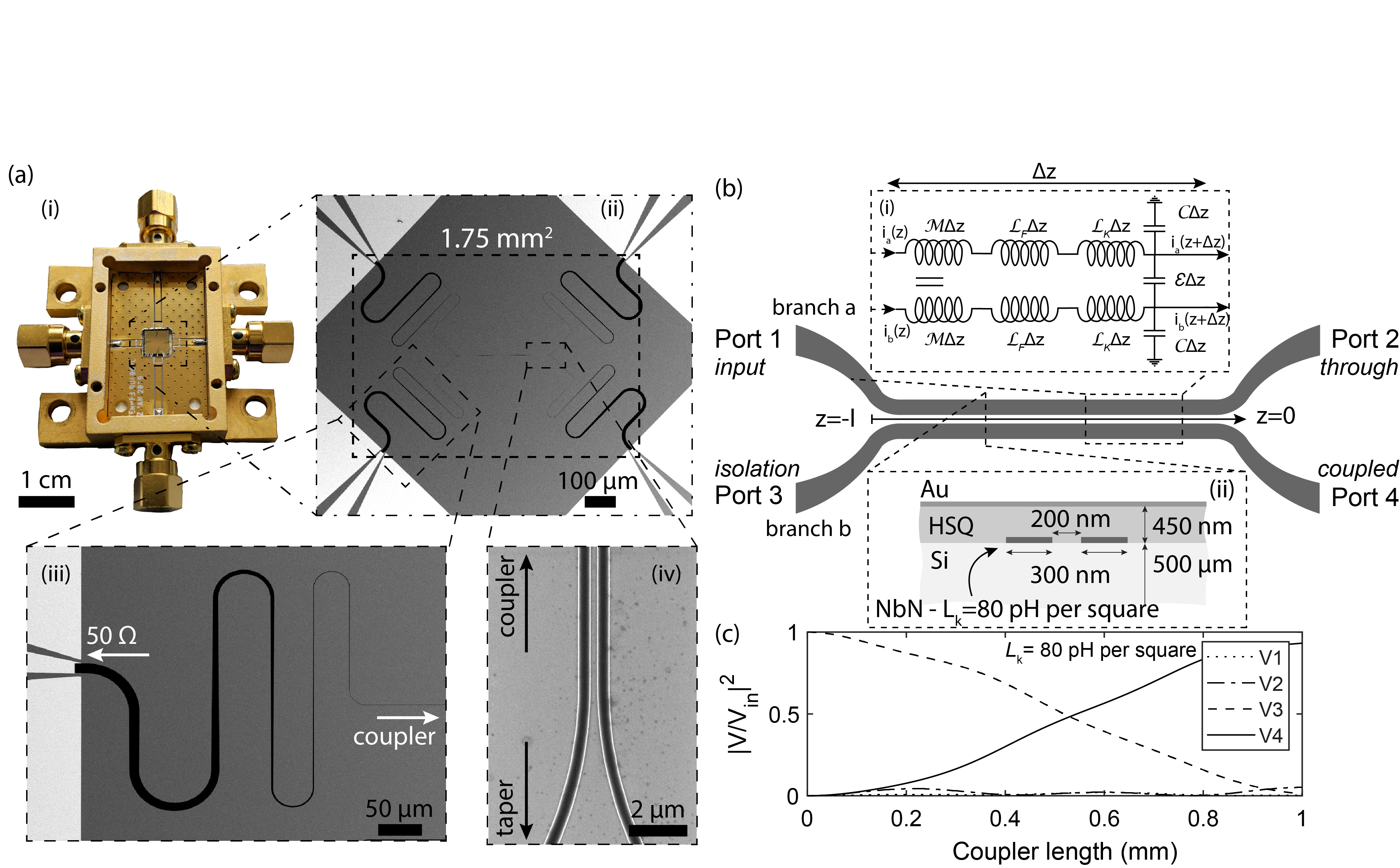
Conventional directional coupler modules split, combine and distribute microwave fields to the subsequent processing layers or to the readout [15, 30, 31]. They carry out essential processing tasks but take up a significant volume inside the cryostat. Here, we use high kinetic-inductance superconductors to demonstrate a compact high-impedance directional coupler. Our miniaturized coupler is based on niobium nitride (NbN) superconducting nanowire side-coupled striplines embedded in a multilayer dieletric stack. Fig. 1(a) shows optical and scanning electron micrographs (SEM) of the fabricated device. We achieve forward coupling in the GHz range in an extremely reduced footprint and with impedance matching flexibility. We further demonstrate that the non-linear dependence of the nanowire’s kinetic inductance on DC current and temperature allow the microwave properties of the coupler to be tuned. We suggest this device may find immediate application in superconducting quantum computing systems and in other low-temperature applications where small-footprint on-chip coupling at microwave frequency is needed.
Our device is designed following a traditional coupled-line architecture (Fig. 1(b)) where two superconducting nanowires are brought together for a coupling length . The structure can be modeled as a coupled LC ladder (Fig. 1(b)(i)) using a standard coupled-mode formalism [32, 33, 34], with some modifications to capture the kinetic-inductive transmission line [35]. To reflect the high-inductivity behavior of nanowires, we explicitly separate the kinetic contribution (), from the geometric (Faraday) contribution () to the total line inductance per unit length. The coupling produces mode splitting into common () and differential () modes, with different effective indices and propagation constants ( and ). In a transmission line, a sinusoidal signal with frequency is a superposition of these eigenmodes and energy is continuously transferred between the two lines with a periodicity . A section of coupled transmission line with a length that is an odd-integer multiple of can perform, in the ideal case, forward coupling at . In RF transmission lines made of conventional materials, the splitting in propagation constant is relatively small and the minimum length required to achieve forward coupling (at a target frequency) is relatively large. Therefore, it is generally more convenient to exploit the difference in the characteristic impedance of the eigenmodes to realize low-coupling backward directional couplers [33, 36]. With coupled superconducting nanowires, the combination of high-kinetic inductance lines, high coupling capacitance, and low loss boosts and allows forward coupling in a small footprint ( is relatively small). Moreover, backward reflections can be minimized by gradually tapering the exits from the coupled-line section (Fig. 1(a)(iv)). See Supplemental Material (SM) for the full derivation of the model.
To practically illustrate this concept, we consider the side-coupled stripline implementation, shown in Fig. 1(b)(ii), which we used to realize our device. The lines are made of a -wide, -thick NbN nanowire with a sheet kinetic inductivity of per square, separated by a wide gap. The structures are patterned on silicon and referenced to a topside gold ground plane through a thick hydrogen silsequioxane (HSQ) dielectric layer, with [37, 38]. In this microwave environment, the simulated characteristic impedance is and the effective index , which reduces the phase velocity to of and highly compresses the guided wavelength. See SM for details on the simulations. For clarity, the port naming convention is shown in Fig. 1(b). Fig. 1(c) shows that a signal injected through the input port of the coupling section takes to forward couple 50% of the power to the other branch. Compared to the same structure realized with conventional conductors [39], this coupling section achieves almost two orders of magnitude footprint reduction (see SM).
The device was fabricated with parameters based on the modeling results. See SM for details on the fabrication. Fig. 1(a) shows micrographs of the device before the fabrication of the dielectric spacer and the top ground. In the final design we used a coupling length and we included four high-pass Klopfenstein impedance-matching tapers (Fig. 1(a)(iii)) [40, 41, 38, 42, 43]. Coplanar waveguide (CPW) signal feed lines ( gold) were also fabricated to allow wire-bonding and packaging. The footprint of the full superconducting structure (as outlined in Fig. 1(a)(ii)) was , while the high-impedance coupling section only occupied .
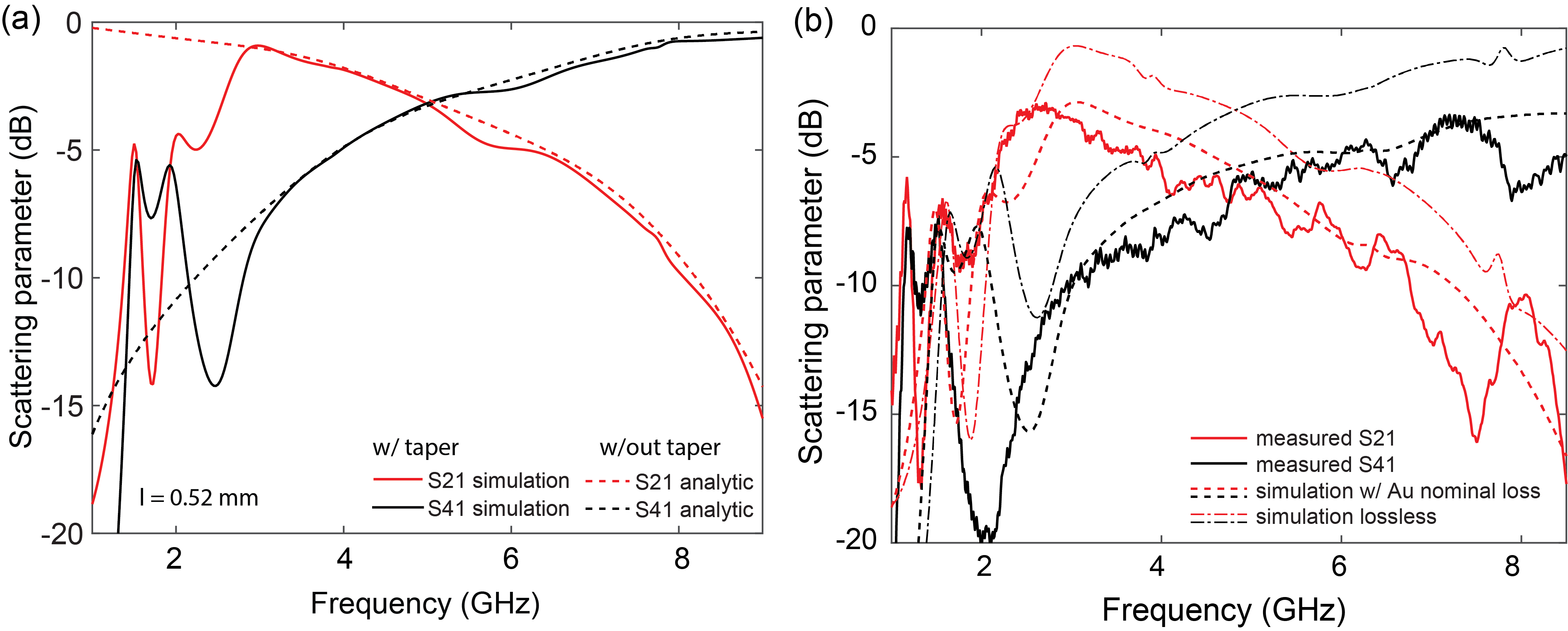
The addition of the tapers, while increasing the total footprint of the device, improves flexibility, affording the possibility to interface the high-impedance coupling section to lower-impedance environments without disturbing the forward coupling operation. In this case we interfaced the high-impedance nanowire transmission line coupler to RF electronics. Fig. 2(a) shows that, in the taper passband (), the simulation results (full wave) of the impedance-matched coupler correctly reproduce the analytic calculation of the high-impedance coupling section response. The 50% coupling point is at , with the isolation parameter at . See SM for details on the simulations.
We measured the microwave response of the fabricated coupler at with a vector network analyzer providing effective signal power lower than . In the same cooldown, we calibrated the cable and connector loss (cryostat to device box inputs/outputs) to scale the measured data. Fig. 2(b) shows that the forward coupling behavior is observed. At , the input signal from Port 1 couples equally to the through port (Port 2) and forward-coupling port (Port 4) with a level of , and the isolation parameter . For comparison, we show simulations of the impedance-matched coupler, including the response of the feed lines, and corrected to account for fabrication non-idealities (see SM for additional details). The slight discrepancy () between the measured and simulated coupling frequency can be attributed to the uncertainties in the device parameters. For example, the fabrication process, consisting of several lithographic and etching steps, may induce a degradation of the film leading to an increase in the kinetic inductance that would explain this observation. We attribute the inconsistency in the magnitude of the S parameters to backward reflections, device-level conductor losses, and to additional contributions that were not accounted for in the calibration. In this experiment, the calibration does not account for losses and reflection from the sample holder PCB and wire bonds. The agreement with the simulation improves when we include normal conductor losses for the Au layers. More details can be found in the SM. The isolation parameter is at a significantly different level from the expected value. This discrepancy might be caused by factors such as the impedance-matching taper deviating from the prescribed design, with sub-optimal impedance matching and additional backward reflections, and the specific full device simulation not including element-to-element transitions (e.g. stripline to CPW). See SM for additional details.
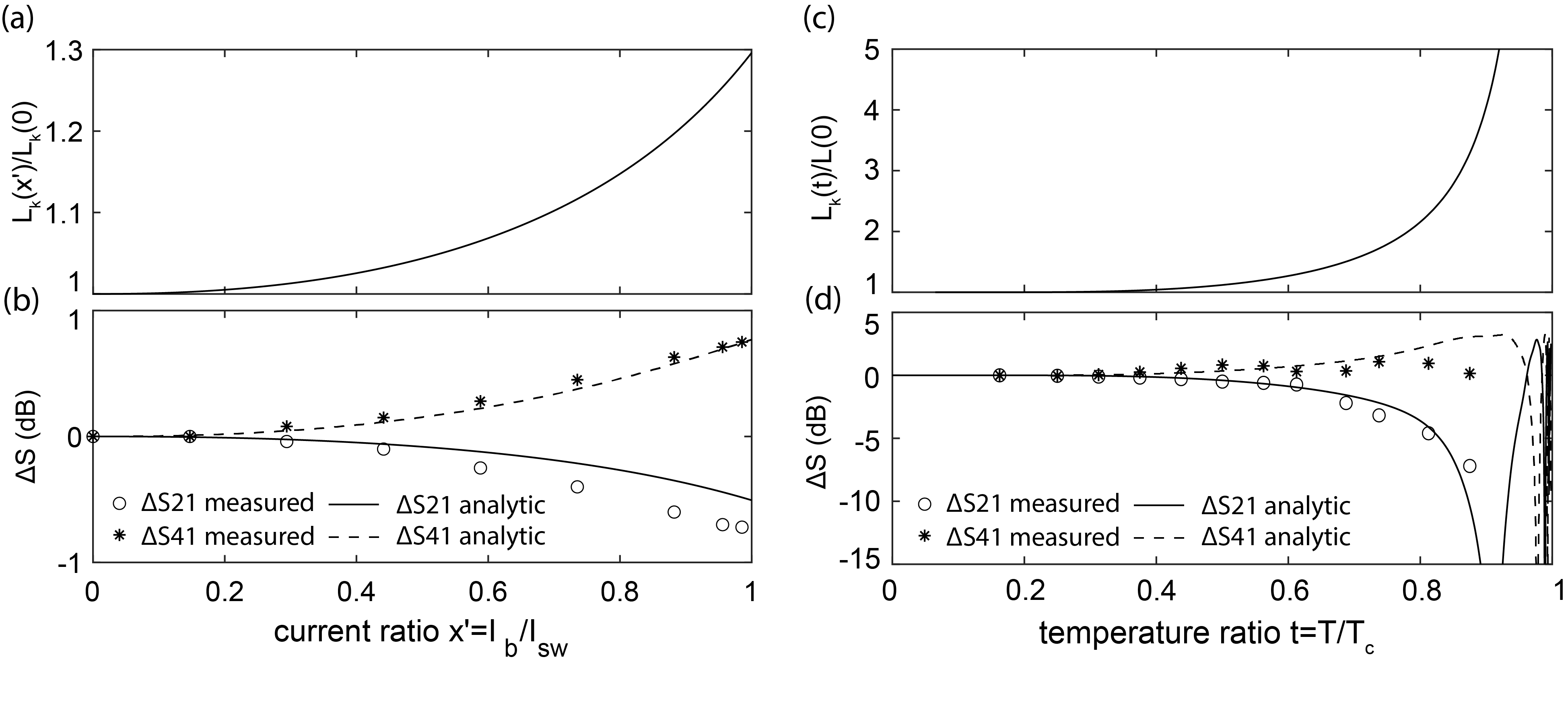
The microwave response was characterized with effective injected currents much smaller than the device depairing current (see SM). In this small-signal condition the device response is independent of the applied microwave power. However, the kinetic inductance strongly depends on carrier density, which can be tuned with current () and with temperature (): , where is the switching current and is the critical temperature. Leveraging these dependencies affords the possibility of dynamically modulating the microwave characteristics of the modes in the lines, creating active, tunable devices. When the bias current in the nanowire approaches the depairing current (), the kinetic inductance diverges hyperbolically , with determined by the operating temperature of the device [44]. Due to fabrication imperfections, superconducting nanowire devices similar to the ones described in this paper typically can only reach a fraction of the depairing current, with the switching current [45]. Fig. 3(a) shows that with this assumption and given the measurement condition () [44], a theoretical maximum increment of the kinetic inductance might be expected. In the coupled-line architecture the two nanowires are galvanically isolated. Hence, the kinetic inductance of each nanowire can be tuned independently. We characterized the device tunability at by biasing the coupler through the isolation port and measuring the coupled and transmitted powers. Fig. 3(b) shows the change of scattering parameters with the applied current, in agreement with analytical modeling. The increase of kinetic inductance increases S41 and reduces S21 at the original equal-coupling frequency, which in turn shifts the 50:50 coupling point to a lower frequency (see SM).
When changing the operating temperature, a much wider variation of the kinetic inductance, and hence of the scattering parameters, can be achieved. Fig. 3(c) shows the expected theoretical temperature dependence of the kinetic inductance obtained through numerical calculation of the superconducting gap, and the corresponding kinetic inductance [46, 47], using characteristic values for NbN [48]. We characterized the coupling tunability by varying the base temperature of the cryostat and measuring the S21 and S41, at . With this measurement setup, the variation of the temperature modulates the kinetic inductance of both the nanowires. Fig. 3(d) shows tunability of the parameters with temperature and is in fair agreement with the model. The observed discrepancies with the theoretical curves are attributed to the uncertainty in the modeling parameters used for the calculation of . Moreover, as the calculation only includes the coupling section, the impact of other elements of the device (e.g. tapers) was not captured. Note that when the kinetic inductance is far from the design value, the microwave characteristics of the taper can significantly diverge from the intended behavior.
The device presented in this work achieves 50:50 forward coupling in a dramatically reduced footprint by exploiting the properties of high-inductance superconducting nanowire transmission lines. The coupling section, as configured here, occupies only and can be integrated as-is in high-impedance environment circuits with . Moreover, as the characteristic-impedance depends strongly on the device geometry, the device can be matched to a wide variety of high-impedance environments by redesigning the coupling section’s width and length, while keeping a small footprint. As mentioned above, the possibility of performing impedance matching using tapered structures allows one to interface the directional coupler to lower-impedance environment as well. The total occupied footprint, even including the tapers, is still lower than other conventional normal-conductor coupler designs, such as hybrid, Lange, or parallel lines [33], which require . Additional footprint reduction may be achieved by optimizing the packing of current layouts, or by using a higher effective-index transmission-line architecture [41]. Alternatively, a broadside-coupler architecture might be realized allowing an increase of the capacitive coupling and a further reduction of the coupling length (SM).
The model developed to support the design of the device is in agreement with the measured response. The disagreement with the measured data, observed in the magnitude of the scattering parameters, are partially due to backward reflections and to device-level losses which are not accounted for in the system calibration. The effects induced by the use of normal conductors (feed lines and ground plane) or lossy dielectrics can be addressed by redesigning the material stack and adapting the layout. The device model also does not include the power-dependent non-linear effects that might play an additional role when driving the coupler in the highly non-linear kinetic-inductance regime. This could contribute to the discrepancies observed when testing the coupler for , where t is the reduced temperature. The study of the non-linearities in high-kinetic-inductance transmission lines is beyond the scope of this paper.
The tunability of the coupling parameters opens up the opportunity for the realization of high-impedance tunable microwave devices. For example, a high-impedance single-pole double-throw non-linear switch could be realized based on this coupler architecture. Similarly, tunability with temperature may become practical if a heater element is fabricated in close proximity to the coupling section.
We suggest this device may find application in existing superconducting quantum architectures, where the integration of superconducting nanowires, in the form of superinductors, has already been demonstrated [28, 29, 49]. A high-impedance cryogenic tunable coupler could be used for tunable qubit-qubit coupling [50], on-chip integration of novel readout techniques [51], and on-chip signal processing and multiplexing, drastically reducing the necessary wiring from couplers and splitter on the higher temperature stage to the processor at mK. In the effort to scale the size of single-photon detectors arrays, this device could be used to implement architectures based on frequency-multiplexing readout [52, 53]. Further development of this nanowire-based technology may lead to the realization of a family of ultra-compact microwave devices that form the basis of a new superconducting nanowire monolithic microwave integrated circuit technology.
See Supplemental Material for more details on modeling, simulation, fabrication and measurements. All files related to a published paper are stored as a single deposit and assigned a Supplemental Material URL. This URL appears in the article’s reference list.
Acknowledgements.
We thank K. O’Brien, K. Peng, M. Naghiloo for helpful discussions. We thank E. Toomey, J. Simonaitis, and M. Bionta for critical reading of the manuscript. Support for this work was provided in part by the National Science Foundation grants under contract No. ECCS-2000743 and ECCS-2000778 (UNF), and by the Army Research Office (ARO) under Cooperative Agreement Number W911NF-16-2-0192. The views and conclusions contained in this document are those of the authors and should not be interpreted as representing the official policies, either expressed or implied, of the Army Research Office or the U.S. Government. The U.S. Government is authorized to reproduce and distribute reprints for Government purposes notwithstanding any copyright notation herein. Di Zhu was supported by the National Science Scholarship from A*STAR, Singapore, and Harvard Quantum Initiative Postdoctoral Fellowship.References
- Blais et al. [2020] A. Blais, S. M. Girvin, and W. D. Oliver, Quantum information processing and quantum optics with circuit quantum electrodynamics, Nat. Phys. 16, 247 (2020).
- Arute et al. [2019] F. Arute, K. Arya, R. Babbush, D. Bacon, J. C. Bardin, R. Barends, R. Biswas, S. Boixo, F. G. Brandao, D. A. Buell, et al., Quantum supremacy using a programmable superconducting processor. Nature 574, 505–510 (2019), Nature 574, 505 (2019).
- Gambetta et al. [2017] J. M. Gambetta, J. M. Chow, and M. Steffen, Building logical qubits in a superconducting quantum computing system, npj Quantum Inf. 3, 1 (2017), arXiv:1510.04375 .
- Holzman and Ivry [2019] I. Holzman and Y. Ivry, Superconducting Nanowires for Single‐Photon Detection: Progress, Challenges, and Opportunities, Adv. Quantum Technol. 2, 1800058 (2019).
- Fagaly [2006] R. Fagaly, Superconducting quantum interference device instruments and applications, Review of Scientific Instruments 77, 101101 (2006).
- Buchner et al. [2018] M. Buchner, K. Höfler, B. Henne, V. Ney, and A. Ney, Tutorial: Basic principles, limits of detection, and pitfalls of highly sensitive SQUID magnetometry for nanomagnetism and spintronics, J. Appl. Phys. 124, 161101 (2018).
- Zmuidzinas [2012] J. Zmuidzinas, Superconducting microresonators: Physics and applications, Annu. Rev. Condens. Matter Phys. 3, 169 (2012).
- McHugh et al. [2012] S. McHugh, B. A. Mazin, B. Serfass, S. Meeker, K. O’Brien, R. Duan, R. Raffanti, and D. Werthimer, A readout for large arrays of microwave kinetic inductance detectors, Rev. Sci. Instrum. 83, 44702 (2012), arXiv:1203.5861 .
- Bardin et al. [2019] J. C. Bardin, E. Jeffrey, E. Lucero, T. Huang, O. Naaman, R. Barends, T. White, M. Giustina, D. Sank, P. Roushan, K. Arya, B. Chiaro, J. Kelly, J. Chen, B. Burkett, Y. Chen, A. Dunsworth, A. Fowler, B. Foxen, C. Gidney, R. Graff, P. Klimov, J. Mutus, M. McEwen, A. Megrant, M. Neeley, C. Neill, C. Quintana, A. Vainsencher, H. Neven, and J. Martinis, A 28nm Bulk-CMOS 4-to-8GHz 2mW Cryogenic Pulse Modulator for Scalable Quantum Computing, in Dig. Tech. Pap. - IEEE Int. Solid-State Circuits Conf., Vol. 2019-February (IEEE, 2019) pp. 456–458, arXiv:1902.10864 .
- Patra et al. [2018] B. Patra, R. M. Incandela, J. P. Van Dijk, H. A. Homulle, L. Song, M. Shahmohammadi, R. B. Staszewski, A. Vladimirescu, M. Babaie, F. Sebastiano, and E. Charbon, Cryo-CMOS Circuits and Systems for Quantum Computing Applications, IEEE J. Solid-State Circuits 53, 309 (2018).
- Hornibrook et al. [2015] J. M. Hornibrook, J. I. Colless, I. D. Conway Lamb, S. J. Pauka, H. Lu, A. C. Gossard, J. D. Watson, G. C. Gardner, S. Fallahi, M. J. Manfra, and D. J. Reilly, Cryogenic control architecture for large-scale quantum computing, Phys. Rev. Appl. 3, 24010 (2015), arXiv:1409.2202 .
- Borodulin et al. [2019] P. Borodulin, N. El-Hinnawy, A. L. Graninger, M. R. King, C. R. Padilla, L. N. Upton, R. T. Hinkey, T. E. Schlesinger, A. A. Pesetski, M. E. Sherwin, and R. M. Young, Operation of a Latching, Low-Loss, Wideband Microwave Phase-Change Switch Below 1 K, J. Low Temp. Phys. 194, 273 (2019).
- Ruffino et al. [2019] A. Ruffino, Y. Peng, F. Sebastiano, M. Babaie, and E. Charbon, A 6.5-ghz cryogenic all-pass filter circulator in 40-nm cmos for quantum computing applications, in 2019 IEEE Radio Frequency Integrated Circuits Symposium (RFIC) (IEEE, 2019) pp. 107–110.
- Pechal et al. [2016] M. Pechal, J. C. Besse, M. Mondal, M. Oppliger, S. Gasparinetti, and A. Wallraff, Superconducting Switch for Fast On-Chip Routing of Quantum Microwave Fields, Phys. Rev. Appl. 6, 24009 (2016).
- Ku et al. [2011] H. S. Ku, F. Mallet, L. R. Vale, K. D. Irwin, S. E. Russek, G. C. Hilton, and K. W. Lehnert, Design and testing of superconducting microwave passive components for quantum information processing, IEEE Trans. Appl. Supercond. 21, 452 (2011), arXiv:1010.3232 .
- Leonard et al. [2019] E. Leonard, M. A. Beck, J. Nelson, B. G. Christensen, T. Thorbeck, C. Howington, A. Opremcak, I. V. Pechenezhskiy, K. Dodge, N. P. Dupuis, M. D. Hutchings, J. Ku, F. Schlenker, J. Suttle, C. Wilen, S. Zhu, M. G. Vavilov, B. L. Plourde, and R. McDermott, Digital Coherent Control of a Superconducting Qubit, Phys. Rev. Appl. 11, 14009 (2019), arXiv:1806.07930 .
- Brummer et al. [2011] G. Brummer, R. Rafique, and T. A. Ohki, Phase and amplitude modulator for microwave pulse generation, IEEE Trans. Appl. Supercond. 21, 583 (2011).
- Chapman et al. [2016] B. J. Chapman, B. A. Moores, E. I. Rosenthal, J. Kerckhoff, and K. W. Lehnert, General purpose multiplexing device for cryogenic microwave systems, Appl. Phys. Lett. 108, 222602 (2016), arXiv:1603.02716 .
- Naaman et al. [2017] O. Naaman, J. A. Strong, D. G. Ferguson, J. Egan, N. Bailey, and R. T. Hinkey, Josephson junction microwave modulators for qubit control, J. Appl. Phys. 121, 73904 (2017), arXiv:1610.07987 .
- Naaman et al. [2016] O. Naaman, M. O. Abutaleb, C. Kirby, and M. Rennie, On-chip Josephson junction microwave switch, Appl. Phys. Lett. 108, 112601 (2016), arXiv:1512.01484 .
- Abdo et al. [2017] B. Abdo, M. Brink, and J. M. Chow, Gyrator Operation Using Josephson Mixers, Phys. Rev. Appl. 8, 34009 (2017), arXiv:1702.01149 .
- Lowell et al. [2016] P. J. Lowell, J. A. Mates, W. B. Doriese, G. C. Hilton, K. M. Morgan, D. S. Swetz, J. N. Ullom, and D. R. Schmidt, A thin-film cryotron suitable for use as an ultra-low-temperature switch, Appl. Phys. Lett. 109, 142601 (2016).
- Wagner et al. [2019] A. Wagner, L. Ranzani, G. Ribeill, and T. A. Ohki, Demonstration of a superconducting nanowire microwave switch, Appl. Phys. Lett. 115, 172602 (2019), arXiv:1910.09614 .
- Masluk et al. [2012] N. A. Masluk, I. M. Pop, A. Kamal, Z. K. Minev, and M. H. Devoret, Microwave characterization of josephson junction arrays: Implementing a low loss superinductance, Phys. Rev. Lett. 109, 137002 (2012).
- Groszkowski et al. [2018] P. Groszkowski, A. D. Paolo, A. L. Grimsmo, A. Blais, D. I. Schuster, A. A. Houck, and J. Koch, Coherence properties of the 0- qubit, New J. Phys. 20, 43053 (2018).
- Kjaergaard et al. [2019] M. Kjaergaard, M. E. Schwartz, J. Braumüller, P. Krantz, J. I.-J. Wang, S. Gustavsson, and W. D. Oliver, Superconducting qubits: Current state of play, Annu. Rev. Condens. Matter Phys. 11 (2019).
- Grünhaupt et al. [2019] L. Grünhaupt, M. Spiecker, D. Gusenkova, N. Maleeva, S. T. Skacel, I. Takmakov, F. Valenti, P. Winkel, H. Rotzinger, W. Wernsdorfer, A. V. Ustinov, and I. M. Pop, Granular aluminium as a superconducting material for high-impedance quantum circuits, Nat. Mater. 18, 816 (2019), arXiv:1809.10646 .
- Hazard et al. [2019] T. M. Hazard, A. Gyenis, A. Di Paolo, A. T. Asfaw, S. A. Lyon, A. Blais, and A. A. Houck, Nanowire Superinductance Fluxonium Qubit, Phys. Rev. Lett. 122, 10504 (2019), arXiv:1805.00938 .
- Niepce et al. [2019] D. Niepce, J. Burnett, and J. Bylander, High kinetic inductance nbn nanowire superinductors, Physical Review Applied 11, 044014 (2019).
- Gu et al. [2017] X. Gu, A. F. Kockum, A. Miranowicz, Y. xi Liu, and F. Nori, Microwave photonics with superconducting quantum circuits, Phys. Rep. 718-719, 1 (2017), arXiv:1707.02046 .
- Krinner et al. [2019] S. Krinner, S. Storz, P. Kurpiers, P. Magnard, J. Heinsoo, R. Keller, J. Lütolf, C. Eichler, and A. Wallraff, Engineering cryogenic setups for 100-qubit scale superconducting circuit systems, EPJ Quantum Technol. 6, 2 (2019), arXiv:1806.07862 .
- Gupta et al. [1996] K. C. Gupta, R. Garg, I. Bahl, and P. Bhartia, Microstrip Lines and Slotlines (Second Edition) (Artech house, 1996).
- M Pozar [2005] D. M Pozar, Microwave Engineering, 3rd (2005).
- Crampagne et al. [1976] R. Crampagne, L. Jinich, and G. Khoo, Asymmetric coupled lines in an inhomogeneous medium, Electron. Lett. 12, 629 (1976).
- Zhu [2019] D. Zhu, Microwave Engineering in Superconducting Nanowires for Single-Photon Detection, Ph.D. thesis, Massachusetts Institute of Technology (2019).
- Morgan and Weinreb [2003] M. Morgan and S. Weinreb, Octave-bandwidth high-directivity microstrip codirectional couplers, in IEEE MTT-S Int. Microw. Symp. Dig., Vol. 2 (IEEE, 2003) pp. 1227–1230.
- Maier [2001] G. Maier, Low dielectric constant polymers for microelectronics (2001).
- Zhu et al. [2018] D. Zhu, Q. Y. Zhao, H. Choi, T. J. Lu, A. E. Dane, D. Englund, and K. K. Berggren, A scalable multi-photon coincidence detector based on superconducting nanowires, Nat. Nanotechnol. 13, 596 (2018), arXiv:1711.10546 .
- Ikäläinen and Matthaei [1987] P. K. Ikäläinen and G. L. Matthaei, Wideband, forward-coupling microstrip hybrids with high directivity, IEEE Trans. Microw. Theory Tech. 35, 719 (1987).
- Klopfenstein [1956] R. W. Klopfenstein, A Transmission Line Taper of Improved Design, Proc. IRE 44, 31 (1956).
- Zhu et al. [2019] D. Zhu, M. Colangelo, B. A. Korzh, Q. Y. Zhao, S. Frasca, A. E. Dane, A. E. Velasco, A. D. Beyer, J. P. Allmaras, E. Ramirez, W. J. Strickland, D. F. Santavicca, M. D. Shaw, and K. K. Berggren, Superconducting nanowire single-photon detector with integrated impedance-matching taper, Appl. Phys. Lett. 114, 42601 (2019), arXiv:1811.03991 .
- Zhao et al. [2017] Q. Y. Zhao, D. Zhu, N. Calandri, A. E. Dane, A. N. McCaughan, F. Bellei, H. Z. Wang, D. F. Santavicca, and K. K. Berggren, Single-photon imager based on a superconducting nanowire delay line, Nat. Photonics 11, 247 (2017).
- Zhu et al. [2020] D. Zhu, M. Colangelo, C. Chen, B. A. Korzh, F. N. Wong, M. D. Shaw, and K. K. Berggren, Resolving photon numbers using a superconducting nanowire with impedance-matching taper, Nano Lett. 20, 3858 (2020).
- Clem and Kogan [2012] J. R. Clem and V. G. Kogan, Kinetic impedance and depairing in thin and narrow superconducting films, Phys. Rev. B - Condens. Matter Mater. Phys. 86, 174521 (2012), arXiv:1207.6421 .
- Frasca et al. [2019] S. Frasca, B. Korzh, M. Colangelo, D. Zhu, A. E. Lita, J. P. Allmaras, E. E. Wollman, V. B. Verma, A. E. Dane, E. Ramirez, A. D. Beyer, S. W. Nam, A. G. Kozorezov, M. D. Shaw, and K. K. Berggren, Determining the depairing current in superconducting nanowire single-photon detectors, Phys. Rev. B 100, 54520 (2019), arXiv:1904.08596 .
- Santavicca et al. [2016] D. F. Santavicca, J. K. Adams, L. E. Grant, A. N. McCaughan, and K. K. Berggren, Microwave dynamics of high aspect ratio superconducting nanowires studied using self-resonance, J. Appl. Phys. 119, 234302 (2016).
- Gallop [2018] J. C. Gallop, SQUIDs, Josephson Eff. Supercond. Electron. (Courier Corporation, 2018) pp. 1–21.
- Polakovic et al. [2018] T. Polakovic, S. Lendinez, J. E. Pearson, A. Hoffmann, V. Yefremenko, C. L. Chang, W. Armstrong, K. Hafidi, G. Karapetrov, and V. Novosad, Room temperature deposition of superconducting niobium nitride films by ion beam assisted sputtering, APL Mater. 6, 76107 (2018), arXiv:1803.02417 .
- Ku et al. [2010] J. Ku, V. Manucharyan, and A. Bezryadin, Superconducting nanowires as nonlinear inductive elements for qubits, Physical Review B 82, 134518 (2010).
- Krantz et al. [2019] P. Krantz, M. Kjaergaard, F. Yan, T. P. Orlando, S. Gustavsson, and W. D. Oliver, A quantum engineer’s guide to superconducting qubits, Appl. Phys. Rev. 6, 21318 (2019), arXiv:1904.06560 .
- Abdo et al. [2019] B. Abdo, N. T. Bronn, O. Jinka, S. Olivadese, A. D. Córcoles, V. P. Adiga, M. Brink, R. E. Lake, X. Wu, D. P. Pappas, and J. M. Chow, Active protection of a superconducting qubit with an interferometric Josephson isolator, Nat. Commun. 10, 1 (2019), arXiv:1810.07234 .
- Doerner et al. [2017] S. Doerner, A. Kuzmin, S. Wuensch, I. Charaev, F. Boes, T. Zwick, and M. Siegel, Frequency-multiplexed bias and readout of a 16-pixel superconducting nanowire single-photon detector array, Appl. Phys. Lett. 111, 32603 (2017).
- Sinclair et al. [2019] A. K. Sinclair, E. Schroeder, D. Zhu, M. Colangelo, J. Glasby, P. D. Mauskopf, H. Mani, and K. K. Berggren, Demonstration of Microwave Multiplexed Readout of DC-Biased Superconducting Nanowire Detectors, IEEE Trans. Appl. Supercond. 29, 1 (2019), arXiv:1905.06880 .