Fanout of 2 Triangle Shape Spin Wave Logic Gates
Abstract
Having multi-output logic gates saves much energy because the same structure can be used to feed multiple inputs of next stage gates simultaneously. This paper proposes novel triangle shape fanout of spin wave Majority and XOR gates; the Majority gate is achieved by phase detection, whereas the XOR gate is achieved by threshold detection. The proposed logic gates are validated by means of micromagnetic simulations. Furthermore, the energy and delay are estimated for the proposed structures and compared with the state-of-the-art spin wave, and and CMOS logic gates. The results demonstrate that the proposed structures provide energy reduction of %-% in comparison to the other 2-output spin-wave devices while having the same delay, and energy reduction of x-x when compared to the and CMOS counterparts while having delay overhead of x-x.
I Introduction
The information technology revolution caused rapid increase of the amount of raw data, together with the requirements of efficient computing platforms for their processing Shah, Steyerberg, and Kent (2018). CMOS downscaling has been efficient to meet these requirements Agarwal et al. (2018); however, CMOS downscaling becomes very difficult due to different walls: (i) leakage wall Mamaluy and Gao (2015), (ii) reliability wall Haron and Hamdioui (2008), and (iii) cost wall Haron and Hamdioui (2008); Mamaluy and Gao (2015), which implies that Moore’s law will come to the end soon. Hence, different technologies have been explored recently, e.g., graphene devices Jiang et al. (2019), memristors Corinto and Forti (2016), and spintronics Agarwal et al. (2018). One of the spintronics technologies is Spin Wave (SW) technology, which stands apart as one of the most promising technologies because Mahmoud et al. (2020, 2020a); Agarwal et al. (2018); Mahmoud et al. (2020b): (i) It consumes ultra-low power because SW computing is based on wave interference without the need for charge movement. (ii) It has an acceptable delay determined by the group velocity of the spin wave. (iii) It is highly scalable because the SW wavelength can reach down to the nanometer range at rf-frequencies. Hence, the design of spin wave based logic gates is of great interest.
Given the potentially low energy consumption of the SW based computing paradigm, a large number of different SW logic gate structures have been presented Schneider et al. (2008); Lee and Kim (2008); Rana and Otani (2018); Khitun and Wang (2011, 2005); Wu et al. (2009); Khitun et al. (2007, 2008); Klingler et al. (2014); Nanayakkara et al. (2014); Shabadi et al. (2010); Kostylev et al. (2005). The first experimental work using SW amplitude detection is considered to be a Mach-Zehnder interferometer based NOT gateKostylev et al. (2005), while XNOR, NAND, NOT, and NOR gates based on a Mach-Zehnder interferometer were also suggested Lee and Kim (2008); Schneider et al. (2008). Furthermore, transmission line based NOT, OR, and AND gates were presented Khitun and Wang (2005)Wu et al. (2009)Khitun et al. (2007)Khitun et al. (2008), and parallel voltage controlled re-configurable nano-channels based XNOR and NAND gates were discussed Rana and Otani (2018). Bent waveguides and transmission lines were utilized to design (N)AND, (N)OR, XOR, Majority Gates Khitun and Wang (2011); Klingler et al. (2014). In addition, it was suggested that a (N)OR gate can be built with a crossbar structure Nanayakkara et al. (2014). However, the previous works’ gates don’t provide more than one output, which is a crucial gate feature for an efficient utilization of SW based technology to build larger circuits. Moreover, if the spin wave logic gate output is taken as input for multiple following logic gates in a circuit, then the logic gate must be replicated multiple times which gives significant energy overhead. While the previously mentioned proposals don’t provide more than one output, it has been suggested in Mahmoud et al. (2020, 2020) that by adding one arm and making use of one extra transducer, a fanout of is achieved. However, this proposal requires an extra cell to excite spin waves and thus again results in energy overhead. Furthermore, the spin waves must be excited at different energy levels which might add energy overhead and complexity to the gate design. In short, the aforementioned designs will add relatively large energy overhead and complexity to the designs in order to achieve the fanout of 2.
The aforementioned limitations are solved in this paper and a Fanout of (FO2) triangle shape -input Majority gate and a 2-input XOR gate are proposed. The fanout is enabled without the need for an extra transducer and all spin waves are excited at the same energy level resulting in a relatively large energy saves. The main contributions of this work are:
-
•
Developing and designing FO2 logic gates: FO2 -input Majority gate is proposed. Also, it is possible to make use of this structure to implement -input (N)AND, and (N)OR gates by making one of the inputs as control input and the other two as data inputs. Moreover, -input X(N)OR structure is proposed by removing the third input.
-
•
Validating the proposed logic gates functionality: MuMax3 software is used to validate the logic gates structures.
-
•
Demonstrating the superiority: The proposed logic gates are evaluated and compared with the state-of-the-art SW, and and CMOS logic gates. The results demonstrate that the proposed logic gates save energy of %-% in comparison with the state-of-the-art SW logic gates while having the same delay. In addition, the proposed SW logic gates provide energy reduction of x-x when compared to the and CMOS counterparts while having delay overhead of x-x.
The rest of the paper is organized as follows. Section II gives the basics and the fundamentals of the spin wave based technologies and the spin wave computing paradigm. The next Section III explains the proposed fanout of 2 Majority and XOR gates. Section IV provides the simulation setup, results and performance evaluation of the proposed gates, in addition to the discussion about variability, and thermal noise effects. Finally, the paper is concluded in Section V.
II SW technology background
This section provides the basic spin-wave theory and spin-wave based computation paradigm.
II.1 Spin Wave Fundamentals
Magnetic materials can be utilized for memory or computing aims by making use of the magnetization state. For instance, spintronic memory device are based on the magnetization orientation which can take two stable states representing either logic 0 or 1. It is also possible to exploit the dynamical behavior of the magnetization. This magnetization dynamics is expressed by equation 1 which is known as the Landau-Lifshitz-Gilbert (LLG) equation Landau and Lifshitz. (1935)Gilbert (2004):
| (1) |
where is the gyromagnetic ratio, the damping factor, the magnetization, the saturation magnetization, and the effective field which is equal to the summation of the external field, the exchange field, the demagnetizing field, and the magneto-crystalline field.
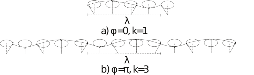
For weak perturbations, equation 1 can be linearised and has wave-like solutions. These solutions are known as spin waves and can be seen as collective excitations of the magnetization. As indicated in Figure 1, SWs are characterized by a wavelength , a wave number (), a phase , an amplitude , and a frequency . The wavelength and frequency respectively characterise the spin precession period in space and in time. The relation between and is the dispersion relation of the wave and is crucial for the design of any spin wave deviceKalinikos and Slavin (1986).
Different spin wave types exist; each with its own features. The direction of wave propagation with respect to the direction of the static magnetization determines which SW type is excited Serga, Chumak, and Hillebrands (2010). These waves are formed when the static magnetization orientation is out-of-plane and results in isotropic spin wave propagation in the plane. Note that this is not the case for the other spin wave types. Therefore, FVSW are promising for circuit design as the same propagation behavior in different directions is required inside the circuit Serga, Chumak, and Hillebrands (2010). While this holds true for many SW based circuit design but some logic elements make use of the non-reciprocity and the anisotropy (non-reciprocity is strongly sought in the acoustic waveguide domain, the spin wave multiplexer makes use of the spin wave anisotropy).
II.2 Spin Wave Computing Paradigm

As any other waves, also SWs interfere with each other. This fundamental phenomenon can be utilized for direct logic function evaluations without requiring the traditional Boolean algebra formalism Mahmoud et al. (2020). Generally speaking, after their generation, multiple SWs coexist and interact in various ways, depending on their amplitude, wavelength, phase, and frequency within the same waveguide Mahmoud et al. (2020). The simplest case, but with the highest practical relevance due to its natural support for majority function evaluation, occurs when SWs with the same amplitude, wavelength, and frequency are interacting Mahmoud et al. (2020). For example, if two such SWs interfere, the resulting SW amplitude is dependent on the phase difference: SWs with the same phase interfere constructively and SWs with different phases interfere destructively, i.e., no output SW is generated, as indicated in Figure 2a. It is clear that if SWs carry digital information this can be processed by means of those interference patterns. For example, the interference of an odd number equal amplitude and wavelength SWs having phases of or results in a majority function evaluation. Note that the Full Adder (a fundamental processor design building block) carry out is computed as a -input majority and most of the error detection and correction schemes rely on -input majorities Mahmoud et al. (2020).
Conceptually speaking, a SW device includes stages: SW creation, propagation, processing, and detection. In the first stage, spin waves are excited in the localised excitation region and then they propagate through the waveguide. When traveling through the waveguide the SW can be manipulated or exposed to different factors within the so-called Functional Region and finally a detector is required to produce the output value Mahmoud et al. (2020); Chumak, Serga, and Hillebrands (2017); Kruglyak, Demokritov, and Grundler (2010). A generic SW device is presented in Figure 2b.
III FO2 SW Logic Gates
In the following lines, the proposed triangle shape fanout of 2 Majority and XOR gates are described.
III.1 Proposed FO2 SW Majority Gate

We developed a novel triangle shape fanout of 2 (FO2) 3-input Majority gate (MAJ3) structure, illustrated in Figure 9. The device consists of 3 inputs , , and corresponding to the excitation cells and 2 outputs and corresponding to the detection cells. Depending on the used method, excitation and detection cells can be voltage encoded or current encoded cells. Many existing options can be used for the excitation and detection cells, e.g., microstrip antennas Mahmoud et al. (2020); Ciubotaru et al. (2016); Chumak, Serga, and Hillebrands (2017), magnetoelectric cells Mahmoud et al. (2020); Cherepov et al. (2014); Chen et al. (2017, 2017); Duflou et al. (2017), spin orbit torques Mahmoud et al. (2020); Talmelli et al. (2018); Gambardella and Miron (2011). In contrast to the ladder shape structure Mahmoud et al. (2020), the proposed triangle shape structure doesn’t need the replication of one of its inputs to enable fanout capability and thus is more energy efficient as will be demonstrated in the performance evaluation subsection (Subsection IV.4).
To simplify the interference pattern, the width of the waveguide must be equal or less than wavelength . All SWs are excited with the same amplitude and frequency to obtain the desired pattern at the interference point. The proposed structure is generic and its dimensions are indicated in Figure 3. The structure dimensions must be chosen accurately to provide the desired functionality. For example, if the desired interference is to constructively interfere if the SWs have the same phase and destructively interfere when SWs are out of phase, then dimensions , and must be n (where n=0,1,2,3,…). Whereas if the opposite behaviour is desired, such that the SWs interfere destructively when they have the same phase and constructively interfere when they are out of phase, then the dimensions , and must be (n+1/2).
The logic gate provides a fan-out of 2 because of the structure symmetry. The outputs and must be captured at the same distance () from the last interference point. Furthermore, this distance must be chosen precisely such that if the desired output has to give logic inversion then must be (n+1/2), whereas if the desired results has to give the non-inverted output then must be n.
The proposed gate operates as follows: (i) At , , and , SWs are excited with the suitable phase ( for logic and phase for logic ). (ii) The excited SWs at and propagate diagonally until reaching the crossing points where they interfere with each other constructively or destructively depending on their phases. (iii) The resulting SWs propagate to interfere constructively or destructively at both interfering points with the SW excited at . (iv) Once the resulted SWs reach the outputs and , they are interpreted by means of phase detection. Depending on a predefined phase, phase detection is performed as follows: a SW phase corresponds to a logic and a phase of to logic . Because of the symmetry and the SWs’ isotropic propagation through this structure, the two SWs reaching and are identical, which means that a fanout of 2 is achieved.
Furthermore, the proposed structure can be utilized to implement (N)AND and (N)OR gates of and if is fixed to logic for (N)AND gate and logic for the (N)OR gate realization.
Moreover, we note that, if only one MAJ3 gate is required the structure can be simplified by removing one of its sides either the right or left one. Also, the gate fan-out capabilities can be extended beyond 2 by using directional couplers Wang et al. (2018) to split the spin wave into multiple arms and using repeaters Dutta et al. (2015) to regenerate a strong SW in the different waveguides. Additionally, more inputs can be added below or above and .

III.2 Proposed FO2 SW XOR Gate
It is interesting to note that the triangle structure is versatile and becomes an XOR gate by removing the third input as depicted in Figure 4. While the operation principle and the design stpdf are the same as in the previous case, threshold-based detection must be utilized to obtain the XOR functionality. The threshold detection is based on a predefined threshold such that if the received SW magnetization is larger than the predefined threshold, this is logic , and logic otherwise. If the XNOR is desired, the condition can be flipped such that if the received SW magnetization is larger than the predefined threshold, this is logic , and logic otherwise.
The same design stpdf hold true for the XOR gate except for the output detection because it depends on threshold detection and thus the SW amplitude is the important one in this case. Therefore, the output must be detected as close as possible from the last interference point and thus must be as small as possible to capture stronger spin wave.
IV Simulation Setup and Results
This section provides the simulation setup, simulation results as well as performance evaluation and discussion about the variability and thermal noise impact.
IV.1 Simulation Setup
We validated the structure by means of MuMax3 Vansteenkiste et al. (2014) simulations using a wide waveguide with thickness of . The spin wave wavelength is chosen to be which is larger than the waveguide width and therefore results in clear interference patterns. Once the wavelength is determined, the dimensions of the device in Figure 3 can be calculated and become =, =, =, and =. Likewise, the dimensions of the device in Figure 3 can be determined to be =, and =. Moreover, from the SW dispersion relation and for ==, a SW frequency of was determined. In addition, the following parameters are used: magnetic saturation =, exchange stiffness =, damping constant =, and perpendicular anisotropy constant = Devolder et al. (2016).
IV.2 Performed Simulations
Two main experiments are performed: (i) FO2 Majority gate implementation, and (ii) FO2 X(N)OR implementation.
-
•
3-input FO2 Majority gate implementation: The three inputs , and are used to generate spin waves that propagate through the waveguide. The interference results are captured at and based on phase detection.
-
•
2-input FO2 X(N)OR implementation: here two inputs and are used instead of three as in the previous case. Threshold detection is utilized to capture the output.
| Cases | ||||
|---|---|---|---|---|
| Cases | |||
|---|---|---|---|
IV.3 Simulation results
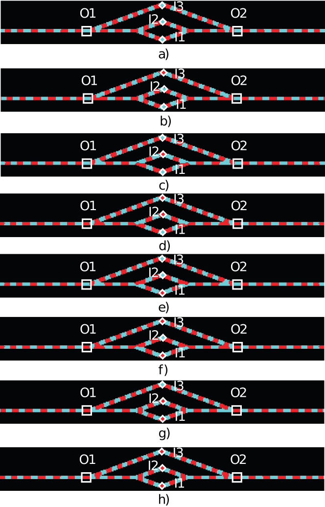
3-input FO2 Majority gate implementation based on phase detection
Figure 5 a to h present the MuMax3 simulation results for the 3-input 2-output Majority gate for {,,}={,,}, {,,},{,,},{,,}, {,,}, {,,}, {,,}, {,,}, and {,,}, respectively, where blue represents logic and red logic . This clearly indicates the correct functionality of the FO2 MAJ3 gate. and provide logic for the input patterns {,,}={,,},{,,},{,,}, and {,,}, whereas they provide logic for the input combinations {,,}={,,},{,,},{,,}, and {,,}.
To demonstrate the equivalence of the two outputs, i.e. FO2 achievement, we extracted the output SWs energy from MuMax3 simulations for all possible input patterns. The normalized magnetization values at and are presented in Table 1. From this table, it is seen that the outputs are the same for all cases, which implies that a fanout of 2 has been successfully achieved.
2-input FO2 X(N)OR implementation based on threshold detection
Table 2 presents the triangle shaped XOR gate normalized magnetization values at the outputs and and for different input combinations {,} {,,,}.
As it is clear from Table 2, an XOR or XNOR logic gate can be implemented if a suitable threshold is chosen to detect logic and logic at the outputs. The appropriate threshold in this case is because for {,} being {,} and {,} magnetization are approximately while they are approximately when the inputs are {,} and {,}. By applying the aforementioned principle to obtain XOR on the data in Table 2, the outputs and are logic at {,}={,} and {,} because their amplitude is larger than and they ( and ) are logic at {,}={,} and {,} because their magnetization are less than . As stated previously, the XNOR can be captured by flipping the condition. Thus, both FO2 XOR and FO2 XNOR can be captured from the proposed structure.
IV.4 Performance Evaluation and Discussion
In this Subsection, we evaluate the energy of the proposed logic gates and discuss the variability and thermal effect.
Performance Evaluation
The proposed -input FO2 XOR and -input FO2 Majority gates are evaluated in terms of energy and delay and compared with the state-of-the-art spin wave Mahmoud et al. (2020, 2020), CMOS Chen et al. (2013), and CMOS Jiang et al. (2018). To evaluate the performance and to make fair comparison with Mahmoud et al. (2020), the following assumptions are made: (i) ME cells are used to excite and detect SWs. (ii) The energy consumption and delay of the ME cells are and , respectively Zografos et al. (2015). (iii) SWs propagation delay in the waveguide is neglected. (iv) SWs propagation loss can be neglected in comparison with the loss in the transducers. (v) The output is passed directly to be used by another SW gate. (vi) Pulse signals are used to excite SWs with pulse duration . Note that the energy consumption in Mahmoud et al. (2020) are re-evaluated based on pulse signal excitation in order to make a fair comparison. Due to the early stage development of SW technology, these assumptions might be optimistic and they might need re-evaluation in the near future.
Furthermore, it was assumed that a -input CMOS Majority gate is built from NAND gates Jiang et al. (2018); Chen et al. (2013). In addition, the energy and delay were estimated with respect to the provided numbers in Jiang et al. (2018); Chen et al. (2013) for the XOR and MAJ gates calculations.
Table 3 presents the evaluation results. As it can be observed from the Table, the proposed Majority gate is x and x slower than the , and CMOS counterparts, respectively, but provides x, and x energy consumption reductions in comparison with , and CMOS counterparts, respectively. Also, the proposed XOR gate saves x, and x energy in comparison with , and CMOS counterparts, respectively, and is x, and x slower than , and CMOS XOR gate. Also, note that SW gates use less number of devices than CMOS which means small real estate chip area. To conclude, SW might lose at the end against CMOS, but the economical benefits will determine which one will win especially that SW technology still is immature technology. Note that assessment and evaluation of complex circuits which were designed using SW technology are available in Zografos et al. (2015). For example, the evaluation results in Zografos et al. (2015) for -bit hybrid CMOS-SW divider showed that the area-delay-power product is x better than -bit divider. This indicates that although SW technology is slow technology but the power and area improvements is much higher and will compensate the slowness Zografos et al. (2015). However, SW technology is still immature technology, and these benchmarks might need re-evaluation in the future.
On the other hand, when comparing with the SW Majority gate Mahmoud et al. (2020), the proposed triangle shape Majority structure saves % energy while keeping the same delay. Also, the proposed XOR structure saves % energy while keeping the same delay when compared with the SW XOR gate in Mahmoud et al. (2020, 2020). This is because of the fact that extra ME cells are required to enable the fanout capability in Mahmoud et al. (2020, 2020). We also note that, for proper gate operation in the ladder shape structure Mahmoud et al. (2020, 2020), inputs may have to be excited at different energy levels depending on whether they have a straight path to the outputs or face bent regions at the edges. In contrast, the proposed triangle shape structure doesn’t require an extra ME cell to achieve the fanout capability, which saves energy and allows for equal energy inputs excitation. Note that the complexity of fabricating such devices are not clear until now due to the early stage development of spin wave based technology.
Variability and Thermal Effect
Validating the proposed logic gates and proofing the concept are the main targets of this paper. Thus, variability and thermal noise effect were not taken into account. However, waveguide trapezoidal cross section and edge roughness effects were examined in Wang et al. (2018); furthermore, it was presented in Wang et al. (2018, 2019) that the gate functionality is correct in their presence. Moreover, thermal noise was introduced in micromagnetic simulations of majority gates Wang et al. (2018, 2019). It was demonstrated that the gates function correctly at different temperatures and the different temperature has only limited impact. Although we expect that the variability and thermal noise will have limited effect on the gate, it will not disturb the gate functionality. We will explore deeply the variability and thermal noise effects on the proposed gates in the near future.
V Conclusions
Novel FO2 spin wave Majority and XOR gates were proposed in this paper. It was demonstrated that by using phase detection, a Majority gate is implemented, whereas the XOR is implemented by threshold detection. Also, the proposed logic gates were validated by means of MuMax3 simulations. The proposed logic gates were assessed and compared with the state-of-the-art spin wave, and and CMOS logic gates. Our evaluation indicated that the proposed logic gates save %-% energy while having the same delay with respect to the state-of-the-art spin wave counterparts. Whereas the result indicated that the proposed logic gates decrease the energy consumption of x-x when compared to the and CMOS counterparts while having delay overhead of x-x.
Acknowledgement
This project has received funding from the European Union’s Horizon 2020 research and innovation program under grant agreement No. 801055 "Spin Wave Computing for Ultimately-Scaled Hybrid Low-Power Electronics" – CHIRON. It has also been partially supported by imec’s industrial affiliate program on beyond-CMOS logic. F.V. acknowledges financial support from the Research Foundation–-Flanders (FWO) through grant No. 1S05719N.
References
- Shah, Steyerberg, and Kent (2018) N. D. Shah, E. W. Steyerberg, and D. M. Kent, JAMA (2018).
- Agarwal et al. (2018) S. Agarwal, G. Burr, A. Chen, S. Das, E. Debenedictis, M. P. Frank, P. Franzon, S. Holmes, M. Marinella, and T. Rakshit, “International roadmap of devices and systems 2017 edition: Beyond cmos chapter.” Tech. Rep. (Sandia National Lab.(SNL-NM), Albuquerque, NM (United States), 2018).
- Mamaluy and Gao (2015) D. Mamaluy and X. Gao, Applied Physics Letters 106, 193503 (2015).
- Haron and Hamdioui (2008) N. Z. Haron and S. Hamdioui, in Design and Test Workshop, 2008. IDT 2008. 3rd International (IEEE, 2008) pp. 98–103.
- Jiang et al. (2019) Y. Jiang, N. C. Laurenciu, H. Wang, and S. D. Cotofana, IEEE Transactions on Nanotechnology 18, 287 (2019).
- Corinto and Forti (2016) F. Corinto and M. Forti, IEEE Transactions on Circuits and Systems I: Regular Papers 63, 1997 (2016).
- Mahmoud et al. (2020) A. Mahmoud, F. Ciubotaru, F. Vanderveken, A. V. Chumak, S. Hamdioui, C. Adelmann, and S. Cotofana, Journal of Applied Physics 128, 161101 (2020), https://doi.org/10.1063/5.0019328 .
- Mahmoud et al. (2020a) A. N. Mahmoud, F. Vanderveken, C. Adelmann, F. Ciubotaru, S. Cotofana, and S. Hamdioui, IEEE Transactions on Circuits and Systems I: Regular Papers , 1 (2020a).
- Mahmoud et al. (2020b) A. Mahmoud, F. Vanderveken, F. Ciubotaru, C. Adelmann, S. Cotofana, and S. Hamdioui, in 2020 Design, Automation Test in Europe Conference Exhibition (DATE) (2020) pp. 642–645.
- Schneider et al. (2008) T. Schneider, A. A. Serga, B. Leven, B. Hillebrands, R. L. Stamps, and M. P. Kostylev, Applied Physics Letters 92, 022505 (2008), https://doi.org/10.1063/1.2834714 .
- Lee and Kim (2008) K.-S. Lee and S.-K. Kim, Journal of Applied Physics 104, 053909 (2008), https://doi.org/10.1063/1.2975235 .
- Rana and Otani (2018) B. Rana and Y. Otani, Phys. Rev. Applied 9, 014033 (2018).
- Khitun and Wang (2011) A. Khitun and K. L. Wang, Journal of Applied Physics 110, 034306 (2011), https://doi.org/10.1063/1.3609062 .
- Khitun and Wang (2005) A. Khitun and K. L. Wang, Superlattices and Microstructures 38, 184 (2005).
- Wu et al. (2009) Y. Wu, M. Bao, A. Khitun, J.-Y. Kim, A. Hong, and K. L. Wang, Journal of Nanoelectronics and Optoelectronics 4, 394 (2009).
- Khitun et al. (2007) A. Khitun, D. E. Nikonov, M. Bao, K. Galatsis, and K. L. Wang, Nanotechnology 18, 465202 (2007).
- Khitun et al. (2008) A. Khitun, M. Bao, Y. Wu, J. Kim, A. Hong, A. Jacob, K. Galatsis, and K. L. Wang, in Fifth International Conference on Information Technology: New Generations (itng 2008) (2008) pp. 1107–1110.
- Klingler et al. (2014) S. Klingler, P. Pirro, T. Brächer, B. Leven, B. Hillebrands, and A. V. Chumak, Applied Physics Letters 105, 152410 (2014), https://doi.org/10.1063/1.4898042 .
- Nanayakkara et al. (2014) K. Nanayakkara, A. Anferov, A. P. Jacob, S. J. Allen, and A. Kozhanov, IEEE Transactions on Magnetics 50, 1 (2014).
- Shabadi et al. (2010) P. Shabadi, A. Khitun, P. Narayanan, M. Bao, I. Koren, K. L. Wang, and C. A. Moritz, in 2010 IEEE/ACM International Symposium on Nanoscale Architectures (2010) pp. 11–16.
- Kostylev et al. (2005) M. P. Kostylev, A. A. Serga, T. Schneider, B. Leven, and B. Hillebrands, Applied Physics Letters 87, 153501 (2005), https://doi.org/10.1063/1.2089147 .
- Mahmoud et al. (2020) A. Mahmoud, F. Vanderveken, C. Adelmann, F. Ciubotaru, S. Hamdioui, and S. Cotofana, AIP Advances 10, 035119 (2020), https://doi.org/10.1063/1.5134690 .
- Mahmoud et al. (2020) A. Mahmoud, F. Vanderveken, C. Adelmann, F. Ciubotaru, S. Cotofana, and S. Hamdioui, in ISVLSI (2020) pp. 60–65.
- Landau and Lifshitz. (1935) L. Landau and E. Lifshitz., Phys. Z. Sowjetunion , 101 (1935).
- Gilbert (2004) T. L. Gilbert, IEEE Transactions on Magnetics 40, 3443 (2004).
- Kalinikos and Slavin (1986) B. A. Kalinikos and A. N. Slavin, Journal of Physics C: Solid State Physics 19, 7013 (1986).
- Serga, Chumak, and Hillebrands (2010) A. A. Serga, A. V. Chumak, and B. Hillebrands, Journal of Physics D: Applied Physics 43, 264002 (2010).
- Chumak, Serga, and Hillebrands (2017) A. V. Chumak, A. A. Serga, and B. Hillebrands, Journal of Physics D: Applied Physics 50, 244001 (2017).
- Kruglyak, Demokritov, and Grundler (2010) V. V. Kruglyak, S. O. Demokritov, and D. Grundler, Journal of Physics D: Applied Physics 43, 264001 (2010).
- Ciubotaru et al. (2016) F. Ciubotaru, T. Devolder, M. Manfrini, C. Adelmann, and I. P. Radu, Applied Physics Letters 109, 012403 (2016), https://doi.org/10.1063/1.4955030 .
- Cherepov et al. (2014) S. Cherepov, P. Khalili Amiri, J. G. Alzate, K. Wong, M. Lewis, P. Upadhyaya, J. Nath, M. Bao, A. Bur, T. Wu, G. P. Carman, A. Khitun, and K. L. Wang, Applied Physics Letters 104, 082403 (2014), https://doi.org/10.1063/1.4865916 .
- Chen et al. (2017) C. Chen, A. Barra, A. Mal, G. Carman, and A. Sepulveda, Applied Physics Letters 110, 072401 (2017), https://doi.org/10.1063/1.4975828 .
- Duflou et al. (2017) R. Duflou, F. Ciubotaru, A. Vaysset, M. Heyns, B. Sorée, I. P. Radu, and C. Adelmann, Applied Physics Letters 111, 192411 (2017), https://doi.org/10.1063/1.5001077 .
- Talmelli et al. (2018) G. Talmelli, F. Ciubotaru, K. Garello, X. Sun, M. Heyns, I. P. Radu, C. Adelmann, and T. Devolder, Phys. Rev. Applied 10, 044060 (2018).
- Gambardella and Miron (2011) P. Gambardella and I. M. Miron, Philosophical Transactions of the Royal Society A: Mathematical, Physical and Engineering Sciences 369, 3175 (2011), https://royalsocietypublishing.org/doi/pdf/10.1098/rsta.2010.0336 .
- Wang et al. (2018) Q. Wang, P. Pirro, R. Verba, A. Slavin, B. Hillebrands, and A. V. Chumak, Science Advances 4 (2018), 10.1126/sciadv.1701517, https://advances.sciencemag.org/content/4/1/e1701517.full.pdf .
- Dutta et al. (2015) S. Dutta, S.-C. Chang, N. Kani, D. E. Nikonov, S. Manipatruni, I. A. Young, and A. Naeemi, in Scientific reports (2015).
- Vansteenkiste et al. (2014) A. Vansteenkiste et al., AIP Advances 4, 107133 (2014).
- Devolder et al. (2016) T. Devolder, J.-V. Kim, F. Garcia-Sanchez, J. Swerts, W. Kim, S. Couet, G. Kar, and A. Furnemont, Phys. Rev. B 93, 024420 (2016).
- Chen et al. (2013) Y. Chen, A. Sangai, M. Gholipour, and D. Chen, in 2013 IEEE/ACM International Symposium on Nanoscale Architectures (NANOARCH) (2013) pp. 82–88.
- Jiang et al. (2018) Y. Jiang et al., in IEEE NANOARCH (2018) pp. 1–7.
- Zografos et al. (2015) O. Zografos, B. Sorée, A. Vaysset, S. Cosemans, L. Amarù, P. Gaillardon, G. D. Micheli, R. Lauwereins, S. Sayan, P. Raghavan, I. P. Radu, and A. Thean, in 2015 IEEE 15th International Conference on Nanotechnology (IEEE-NANO) (2015) pp. 686–689.
- Wang et al. (2019) Q. Wang, B. Heinz, R. Verba, M. Kewenig, P. Pirro, M. Schneider, T. Meyer, B. Lägel, C. Dubs, T. Brächer, and A. V. Chumak, Phys. Rev. Lett. 122, 247202 (2019).