Shadowing effect on the morphologies of thin-films deposited over plane and patterned substrates
Abstract
A simple two-dimensional ballistic deposition (2D-BD) code has been developed to show the geometric shadowing effects in thin-film evolution. A criterion to determine when the shadowing effect dominates over surface diffusion is presented. This code is validated for a plane substrate by comparing the morphological features like the angle of growth, porosity and root mean square (RMS) surface roughness of simulated thin-film deposits with published results. The code is then further validated by applying to two experiments of thin film deposition on (i) a plane substrate with a parallel collimator and (ii) a sinusoidal patterned substrate. In the case of a plane substrate with a parallel collimator, the reported thin-film morphologies ranging from continuous films to nano-islands have been reproduced. For a patterned substrate, the experimentally observed replicability of a substrate topography by the surface of thin-film for normal and oblique angle deposition is ascertained. The code predicts an angle of growth of 565° for an angle of deposition of 77° on patterned substrates, compared to the experiment which reports 50°. This is much better than empirical rules like the tangent rule, which predicts 71° for this case.
keywords:
GLAD , deposition , shadowing effect , tilted columns , replicability , patterned substrate1 Introduction
The thin-film deposition was reported more than 150 years ago by W. R. Grove [1] and M. Faraday [2]. However, a large variety of applications of thin-films in optical, sensor and energy storage devices have been witnessed in the past few decades [3, 4, 5, 6]. This became possible with the advancement of its subclasses such as “Oblique Angle Deposition (OAD)”, “Glancing Angle Deposition (GLAD)”, etc. [7]. OAD is performed typically with a fixed substrate, inclined at any angle to the incoming flux of depositing particles. Whereas in GLAD, which is an extension of OAD, the substrate is fixed at glancing angles that can result in nano-structures, such as inclined, helical or zig-zag columns, etc. [8]. In GLAD, the substrate may also undergo individual or combined effects of change in relative position, inclination or rotation. Use of a collimator or a patterned substrate gives additional freedom to tune the thin-film properties [9, 10].
Ballistic deposition simulations are used to understand the critical growth mechanisms of thin-film evolution and to predict their morphologies [11]. In ballistic deposition (BD), depositing particles are represented by hard spheres which are projected towards a substrate at a chosen angle depending on the source location. The particles are projected one after the other. Each projected particle travels linearly until it either reaches the substrate or it intercepts a previously deposited particle. It is assumed to stick to a particle or substrate with which it makes first contact. During such a deposition, a projected particle can be shadowed by the previously deposited particles. This is called the shadowing effect [12, 13, 14] in thin-film deposition. The initial ballistic deposition simulations of Henderson et al. [12] provide details about the columnar morphology in thin-films. Later, bouncing and relaxation of projected particles [15], surface diffusion and re-emission [16, 17, 18] of deposited particles have been introduced depending on the experimental growth parameters like temperature, energy of the incident particle, etc. Meakin et al. have carried out extensive 2D and 3D ballistic deposition simulations using fractals. They show that the differences in the angle of growth for the 2D and 3D simulations is 3–6° for angles of deposition 60–85° [19, 20]. Ballistic deposition simulations are computationally inexpensive as compared to molecular dynamics (MD) simulations and can simulate much larger sizes of deposits to study the experimentally observable morphological features.
A two-dimensional ballistic deposition code (2D-BD), based on geometric shadowing effect to study the morphological features in thin-film evolution has been developed and it is described in Section 2. Surface diffusion of the deposited particles is not considered. A criterion for neglecting surface diffusion considering the incident fluxes and surface migration energy of deposited particles is presented. The code is validated with published results of angle of growth, porosity and RMS surface roughness for a plane substrates in Section 3.1. It is then further validated by applying it to two experiments in Sections 3.2, 3.3. One experiment [9] demonstrates the tuning of the thin-film morphology using a novel angle constrained glancing angle deposition on a plane substrate with a parallel collimator. The other experiment [10] shows the height to which a patterned substrate topography is replicated by the film surface under normal and oblique angle depositions. Finally, the conclusions are summarized in Section 4.
2 Simulation Method
The present study is limited for cases where the typical time for surface diffusion of a deposited particle is much less than the typical time for deposition of incident particles on it. If is frequency of incident particles depositing on previously deposited particles and is the frequency of the deposited particle making a random jump (diffusion), then,
| (1) |
| (2) |
Here, is the flux of incident particles onto the target and is the cross-sectional area of a deposited particle for an incident particle. The deposited particles diffuse with a typical jump-attempt frequency or phonon frequency () of around . is the migration energy required for surface diffusion of a deposited particle, is the Boltzmann’s constant and T is temperature. The 2D-BD simulations are therefore valid for the following criterion:
| (3) |
The migration energy of a deposited particle depends on the nature of adsorption. In the case of physisorption, adsorbate particles stick with a substrate due to weak Van der Waal forces and have migration energies of the order of 0.1 eV. Chemisorption involves chemical interaction between adsorbate particles and the substrate and has migration energies of the order of 0.9 eV. In case the deposited atoms form chemical bonds (ionic, covalent or metallic) with a substrate, the migration energies can be of the order of 1.5 eV. Assuming the above stated typical values of migration energy, a of 1.5 Å, a substrate temperature of 70 ℃ and typical phonon frequency of , the 2D-BD code will be valid for incident fluxes greater than for physisorption, for chemisorption and for ionic/covalent/metallic bonds. Note that the temperature of the substrate is also an important parameter in the calculation of the criterion for applicability of the code. 2D-BD simulations are carried out to study the thin-film deposition on (i) a plane substrate, (ii) a plane substrate with a parallel collimator and (iii) a sinusoidal patterned substrate. These simulation methods are described below.
In the present study, circular discs of a fixed size are used to represent the particles. These are initialised uniformly, randomly and then projected towards the substrate at a chosen angle of deposition. This angle is chosen by sampling from a Gaussian distribution with the given angle of deposition () and a standard deviation (). Each particle is projected after the deposition of a previously projected particle. A projected particle travels rectilinearly and reaches the substrate or a previously deposited particle. It is assumed to stick to a particle or substrate with which it makes its first contact.
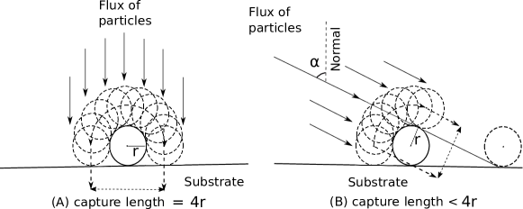
During the normal ballistic deposition, a projected particle can undergo symmetric impingement about a previously deposited particle as shown in Fig 1 (A). This results in dense packing of the particles. In oblique angle deposition, a particle deposited earlier shadows some portion of the deposition area as shown in Fig 1 (B). Due to this, the capture length of particles arriving later will be reduced by the particles that have previously been deposited, resulting in the shadowing effect [12, 13]. With this asymmetric impingement, the mean orientation of the pair of particles shifts towards the normal. This makes the angle of growth () of a thin-film less than the angle of deposition () [13].
2.1 2D Ballistic Deposition on a plane substrate
Particles are initialized uniformly, randomly and then projected towards the substrate at a chosen angle as described before. 2D-BD simulations have been carried out for the angles of deposition ° - ° in steps of °. At each angle of deposition, various standard deviations (°, °, °, °, °) are used to understand the effect of standard deviation on the film growth. In each simulation, one million particles are employed to project on to a substrate of length one micron. To understand the effect of size of particles, simulations are carried out with various particle sizes (r = 1.0 Å, 1.5 Å, 2.0 Å and 2.5 Å) at each angle of deposition. Standard deviation is kept constant (= °) when the effect of size of particles is being studied as a function of the angle of deposition. Furthermore, since the growth is a random process, ten trials of simulations have been carried out for each of these angles of deposition with a standard deviation of 1° and disc radius of 1.5 Å. The typical height of most of the grown films is about . The angle of growth, porosity, RMS surface roughness of the simulated thin-film deposits have been studied as functions of both the angle of deposition and the size of particles. Then the code is validated by comparing these results with published theoretical and experimental results in Section 3.1.
2.2 2D Ballistic Deposition on a plane substrate with a parallel collimator
The collimated glancing angle deposition (C-GLAD) technique is found to be more effective than a simple GLAD for optimizing the microstructure of thin-films [21, 22]. In this technique, a collimator is placed parallel to the substrate at a suitable distance () as shown in Figure 2-(A). With this, the angular spread of depositing flux can be constrained and the maximum tunability in the morphology of the deposition can be achieved. Haque et al. tailored the refractive index of silicon-dioxide thin-film using the C-GLAD technique [23]. Using this technique, they have also shown the tunability of Ag morphology [9]. They demonstrated the change in morphology of Ag deposits from a nearly continuous film to nano-islands of varying size with the increase in the height of a point on the substrate from its bottom edge.
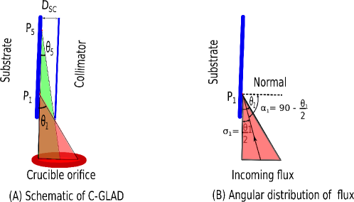
Five equidistant locations (spots) on the substrate have been considered for various characterizations. The distance between any two adjacent spots is 10 mm. Figure 2-(A) shows spots 1 & 5 ( and ) on the substrate and the remaining spots 2–4 (or , , ) are evenly spaced in between spots 1 & 5. It also shows the variation in constrainment of the angular spread of the flux reaching these points. The number of atoms reaching the substrate decreases substantially with the increase in height of the substrate from its bottom edge, due to the increasing constrainment on the incoming flux. More details on this collimated glancing angle deposition experiment can be found in [9].
Five separate simulations have been performed to grow films with the reported thickness mentioned in Table 1. To reproduce the features of spot-1, sufficient number of discs with an angular spread of have to be deposited. To do this, a Gaussian distribution is assumed and deposit sufficient number of discs at an angle of deposition (= 90 - ) with respect to the normal of substrate and with a standard deviation of as shown in Figure 2-(B). Similarly, ballistic deposition simulations have been carried out with the angles of deposition – for the spots 2–5 (–). The parameters used in these simulations are given in Table 1. Different morphological features at different spots have been observed similar to the C-GLAD experiment. These features are discussed in Section 3.2.
| Spot () | = | = | Thickness |
|---|---|---|---|
| 1 | 78.2 | 11.8 | 250 nm |
| 2 | 86.2 | 3.8 | 42 nm |
| 3 | 87.7 | 2.3 | 26.3 nm |
| 4 | 88.4 | 1.6 | 18.4 nm |
| 5 | 88.7 | 1.3 | 16.7 nm |
2.3 2D Ballistic Deposition on a sinusoidal patterned substrate
Keller et al. [10] have deposited nickel (Ni) on a sinusoidal silicon (Si) substrate to study the morphology of thin-film deposition on a sinusoidal patterned substrate. They deposited Ni at an angle of (i) 0° (ii) 77° with respect to the normal of a sinusoidal patterned substrate. The wavelength and the amplitude of the sinusoidal substrate are 35 and 1.5 respectively. They noticed that there is high replicability or conformity of the substrate topography on the surface of deposited film under normal deposition. This replicability reduces with the increase in the height and vanishes at about 120 . In case of glancing angle deposition, they noticed the growth of nanorods bunching together on the more exposed areas of a sinusoidal substrate. These nanorods further grow into anisotropic tilted columns at 7-10 height. These tilted columns start merging with the adjacent structures at about 10 . The replicability of the substrate topography by the film surface reduces with the increase in height and there is no correlation between the substrate and the film surface at about 47 .
2D-BD simulations of thin-film deposition on a sinusoidal substrate are carried out to see if the results produced by Keller et al. [10] can be reproduced just by geometric shadowing effects. In these simulations, circular discs with a radius of 1.24 Å are used to represent Ni particles. These are initialised uniformly, randomly and then projected towards a substrate as mentioned earlier. Note that the experiments used an anisotropic sinusoidal pattern. However, they do not mention the amount of anisotropy. For simplicity, this has been considered as an isotropic sinusoidal substrate with the same periodicity and amplitude as used by Keller et al. Suitable number of particles are projected on to this sinusoidal substrate at (i) 0° and (ii) 77° to attain the reported heights of the film surface. The simulated thin-films are visually analysed for the various reported features at various heights. These results are presented in Section 3.3.
3 Results and Discussion
2D-BD simulations are carried out to study the morphological features of thin-films deposited on (i) a plane substrate, (ii) a plane substrate with a parallel collimator and a (iii) sinusoidal patterned substrate. The results are presented and compared with the available theoretical and experimental results in the following Subsections 3.1–3.3.
3.1 2D Ballistic Deposition on a plane substrate
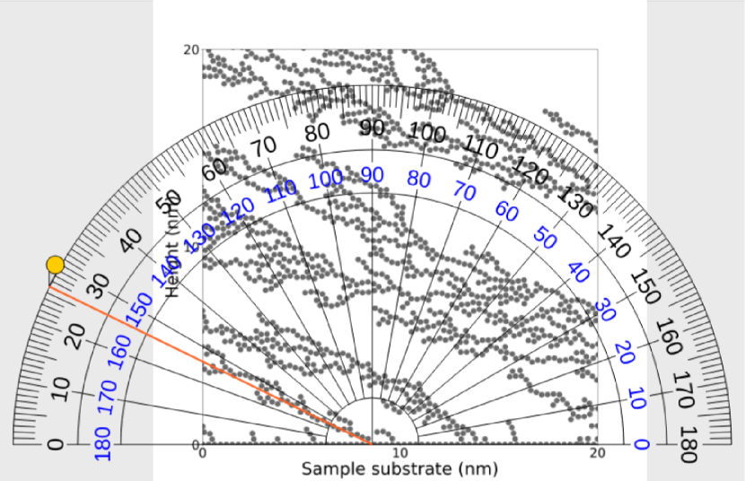
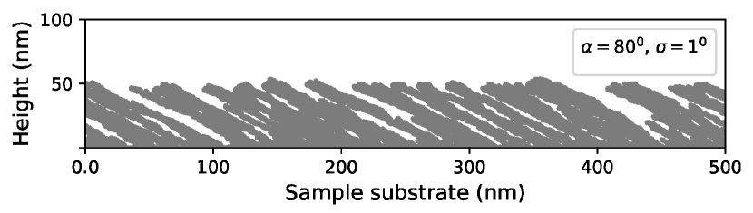
The “tree-like structures” reported earlier at the atomic scales [13, 24, 25] have been observed in all the simulations for all the angles deposition carried out in the present study as seen in Figure.3(a). The height of these structures increases with deposition. The branching of the tree-like structures is more and they are more closely packed at smaller angles of deposition (°, °). Therefore for these angles, a thin-film looks continuous as shown in Figure 3(b). The shadowing effects in a ballistic deposition, increase with the increase in the angle of deposition. With the increasing shadowing effects, the space between the ‘tree-like structures increases. One can see these structures as closely spaced, thin, tilted columns for the angles of deposition °, °. The size and space between these tilted columns increase with the angle of deposition and also with the standard deviation. The tilted columns are easily discernable for angles of deposition °. Figure 3(c) shows the tilted columns formed at an angle of deposition ° with a standard deviation of °. The angle of growth of these tree-like structures or tilted columns is measured using an online protractor tool [26]. In this subsection, angle of growth, porosity and RMS surface roughness of the simulated thin-films on a plane substrate are discussed as a functions of the angle of growth and size of the particles. These are compared with published results to validate the code.
3.1.1 Angle of growth of thin-film
With simple geometric effects, the earlier two-dimensional ballistic deposition simulations could reproduce several key observations such as the angle of growth () is less than the angle of deposition () and a monotonic decrease in the density of thin-film with the increase in the angle of deposition [12, 13, 19]. Various rules have been proposed to describe the relationship between and . We compare our results with widely used “tangent rule” () [27], “cosine rule” () [28].
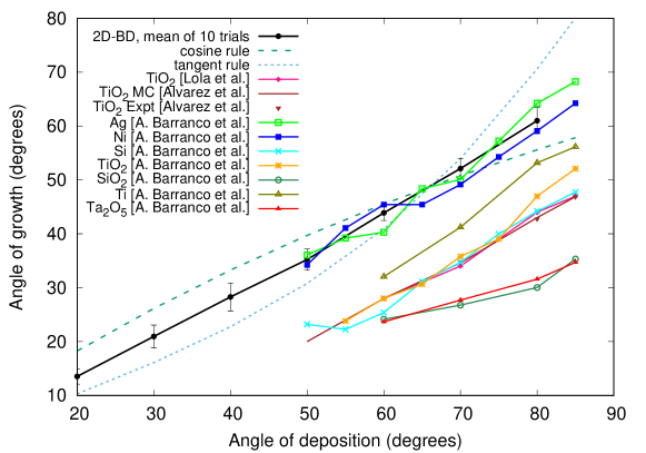
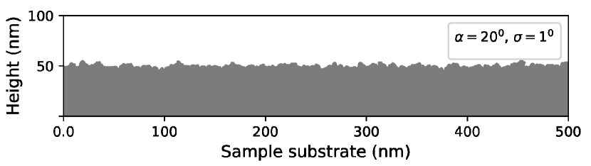
The tilted columns of a thin-film are mostly parallel to each other. The angle of growth of these tilted columns is considered to be the angle of growth of the thin-film. Few columns may not be parallel to the remaining due to “column extinction” at some points due to shadowing effects. The height and orientation of any specific column depend on the orientation and height of the adjacent shadowing columns. In the present study, this issue is taken care of by considering an average value of angles of many tilted columns for each simulation. Further, at each angle of deposition with a standard deviation of °, ten simulations with different random number seeds are carried out. The angle of growth from these ten simulations are obtained as described before and their average value is considered. These angles of growth and their standard deviations are estimated and compared with the available theoretical and experimental results in Figure 4. The angle of growth increases with the angle of deposition. The values of angle of growth are also estimated at each angle of deposition with standard deviations of °, °, °, °, ° to understand the effect of standard deviation in the angle of deposition. It is found that there is no significant change in the angle of growth with the change in standard deviation at a particular angle of deposition.
 |
 |
Figure 4 shows the relationship between the angle of deposition and the angle of growth obtained from the simulations as described above and compares it with the empirical rules [27, 28] and experiments [29, 30, 31, 11]. The mean values of angles of growth from the simulations lie in between the values estimated by tangent and cosine rules. They are found to match closely with the experimental results [30, 11] for pure metals having a cubic lattice structure. They do not match for others either due to preferential direction in bonding or experimental conditions. The angle of growth values from our simulations match the 2D and 3D simulations by Meakin et al [19] within a range of –°. We do not observe any significant change in the angle of growth with the change in the standard deviation, but there are morphological changes like the shape of thin-film deposition, the thickness of tilted columns. Figure 5 shows the increase in the thickness of tilted columns with an increase in the standard deviation.
3.1.2 Porosity
Porous thin-films have a broad spectrum of applications due to their adequate characteristics such as high resistance to thermal shock, low thermal conductivity, etc. Using oblique angle deposition (OAD), one can engineer the required porosity for various applications. In two-dimension:
| (4) |
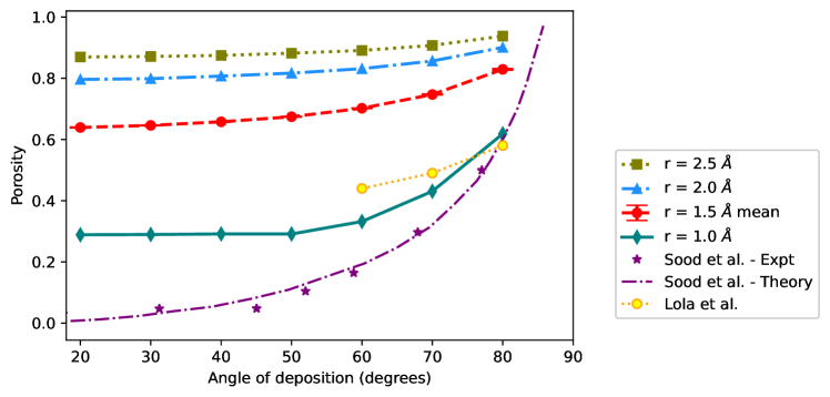
Porosity (P) increases with the angle of deposition [32, 31, 33, 34] and remains constant with the height of the film [35]. Figure 6 shows the porosity (P) as a function of the angle of deposition () and confirms that porosity increases with the increase in the angle of deposition. It can also be seen that porosity increases with an increase in the radius (r) of the particle used in the simulation, which is a geometric effect. The effect of standard deviation () is found to be insignificant at any specific angle of deposition (). Earlier, Sood et al. have used the following expression (5) with a “fitting parameter” () to fit their experimental results with their Monte Carlo simulations for indium tin oxide (ITO) [33].
| (5) |
The results for porosity, reported in the present study, follow the trend observed in experiments. In most of the earlier theoretical studies of ballistic deposition, scaling behaviour of porosity is studied using the particles with unit size [15, 36, 37, 38, 39, 40]. To the best of our knowledge the effect of size of particles on the porosity has not been reported. Here, it is suggested that in simulations, one needs to use the discs of size comparable to that of particles of practical interest, for a quantitative match with the experimental results.
3.1.3 RMS Surface Roughness
Roughness is defined as how the height () of a surface deviates from its average height (). It is measured by finding the root mean square (RMS) variation of the height and is expressed [41] as:
| (6) |
Here, mean height () is estimated for the sampling length of the substrate. To measure the RMS surface roughness (), the surface in the range of sampling length is divided into small bins whose size is equal to the size of the discs. Then mean height () and the root mean square deviation of all heights (RMS surface roughness) are measured for all the simulations carried out in the present study.
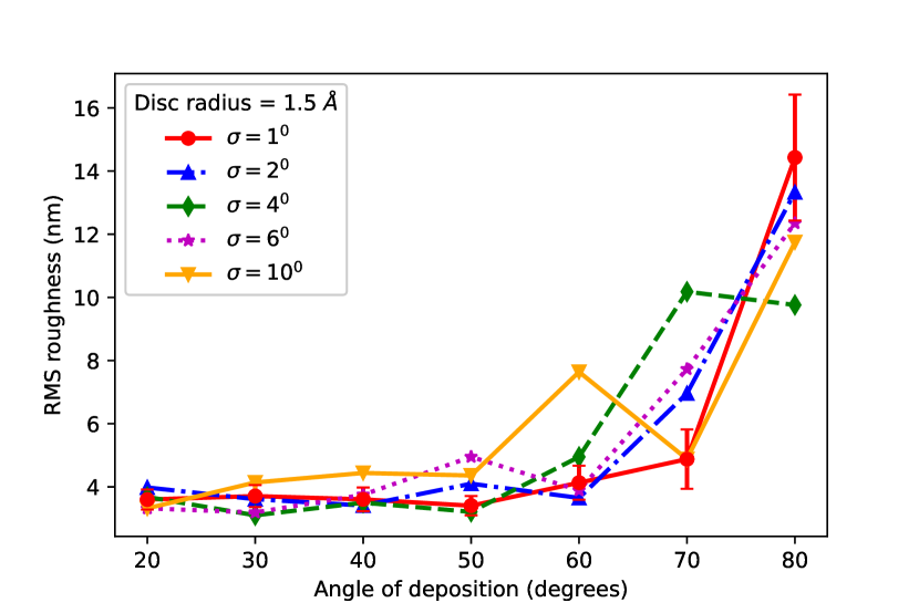
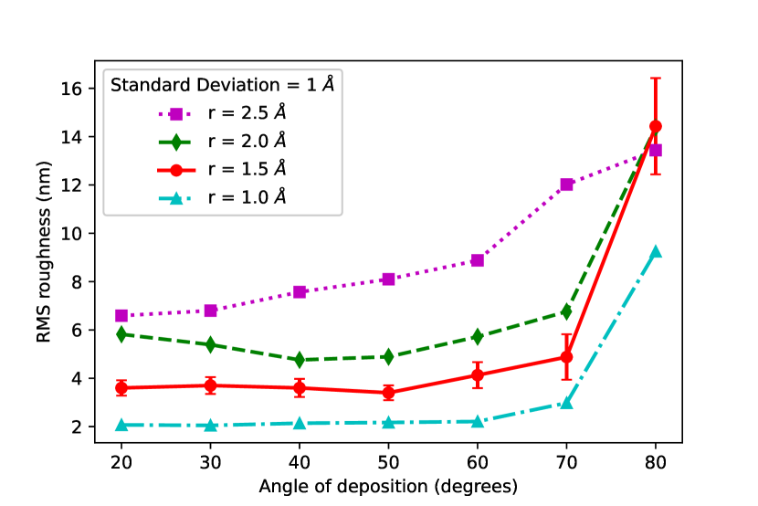
Figure 7(a) shows the RMS surface roughness as a function of the angle of deposition. In general, It is observed that RMS surface roughness increases with the increase in the angle of deposition. To understand the effect of standard deviation on RMS surface roughness, simulations are carried out with discs of a fixed radius equal to 1.5Å using standard deviations 1°, 2°, 4°, 6° and 10°. It can be seen that there is no specific trend for the change in RMS surface roughness with the change in the standard deviation in the angle of deposition. To estimate the statistical error, ten simulations are carried out with ° and the average values are plotted with their statistical error. The change in RMS surface roughness is insignificant for Å. Figure 7(a) shows that the values of RMS surface roughness range from 2-16 nm closely match with the reported range 2-14 nm from the surface analysis of OAD evaporated thin-films by atomic force microscopy (AFM) [11, 41, 42].
To understand the effect of size of the particles on RMS surface roughness, simulations are carried out with the discs of radii equal to 1.0Å, 1.5Å, 2.0Å and 2.5Å. The standard deviation (=1Å) is kept constant at each angle of deposition. Figure 7(b) shows that the RMS surface roughness increases with the increase in the angle of deposition for a given size of the particles. It can also be seen that the RMS surface roughness increases with the increase in the size of particles. Here, the mean values of RMS surface roughness with their statistical error are plotted for the particles of radius equal to 1.5Å.
3.2 2D Ballistic Deposition on a plane substrate with a parallel collimator
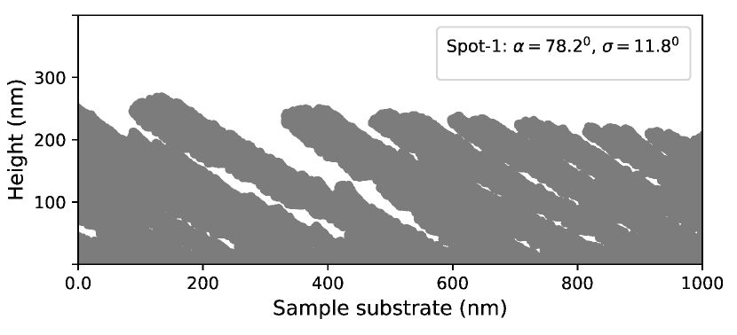
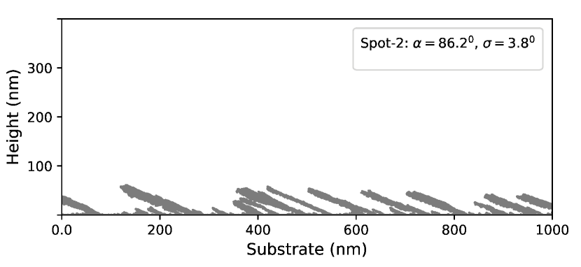
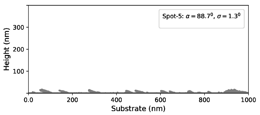
The 2D-BD simulations reproduce similar structures as obtained by Haque et al. [9] and can be seen in Figure 8. In the initial phase of the thin-film growth, small stable clusters of atoms grow into three-dimensional nano-islands. Later, these nano-islands act as growth seeds of nano-rods. These nano-rods further grow to tilted columns resulting in continuous thin-films with protrusions. At spot-1, the film is almost continuous due to larger deposition. At spot-2, it has nanorod structures with reduced deposition. From spot-3 onwards with further reduction in the beam deposition, only discrete nano-islands form and they do not grow large enough to merge and form a continuous film within the allowed deposition time. The observed sizes are compared with the reported sizes from the C-GLAD experiment in Table 2. Porosity for the spots- 1 & 2 are estimated to be 0.79 and 0.96. RMS surface roughness of these first and second spots are 11.25 nm, 12.04 nm respectively for the sampling lengths from 0.0–200 . Porosity and RMS surface roughness characterizations are not considered for the other spots as they are very small individual nano-islands. The number of the individual nano-islands per micron length for the spots 3–5 are about 12, 16, 13 and 15, 21, 18 in the 2D-BD simulations and C-GLAD respectively.
| Spot | Nature | Average | Average | Average spaces | Average spaces |
|---|---|---|---|---|---|
| of the | Reported size | Observed size | between C-GLAD | between 2D-BD | |
| nanostructure | in C-GLAD | in 2D-BD | nanostructures | nanostructures | |
| 1 | Continuous | – | – | protrusions are | protrusions are |
| with protrusions | contiguous | contiguous | |||
| 2 | elongated | nm | 116 nm | nm | |
| nanorods | |||||
| 3 | isolated | nm | 55 nm | nm | |
| nano-islands | |||||
| 4 | isolated | nm | 30 nm | nm | |
| nano-islands | |||||
| 5 | isolated | nm | 30 nm | nm | |
| nano-islands |
The 2D-BD simulations could reproduce the morphology of five equidistant spots in the C-GLAD experiment ranging from continuous thin-film to small individual nano-islands. There is a decent quantitative match for the average sizes of the nano-structures and the average spaces between them. The values of the linear density of number of nano-islands obtained in the 2D-BD simulations for spots 3–5 are within the range of their values obtained in the C-GLAD experiment. The results of 2D-BD simulations have a good match with the results of C-GLAD experiment.
3.3 2D Ballistic Deposition on a sinusoidal patterned substrate
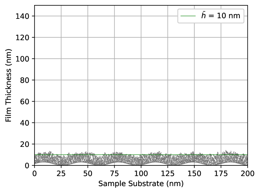
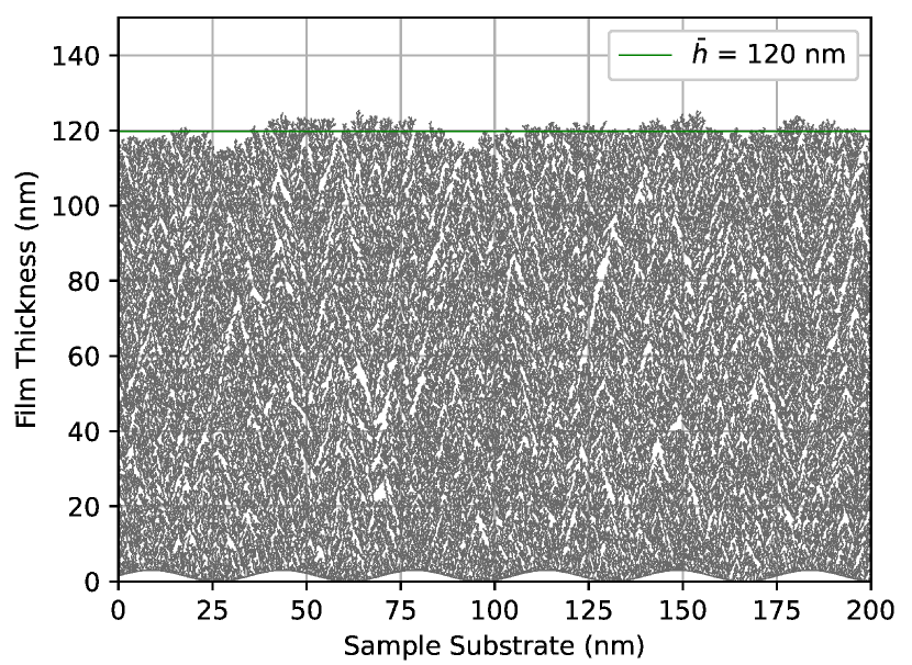
2D-BD simulations of thin-film deposition are carried out at 0°, 77° on a sinusoidal substrate. In case of normal deposition, there is high replicability or conformity of substrate topography by the film surface and it is observed up to a height of about 10 as shown in Figure 9(a). The reported reduction in both the replicability and amplitude of the surface modulation with the increase in height of the film surface have been observed. This is due to the increase in the surface roughness with increasing height. The replicability gradually decreases up to a height of 120 as shown in Figure 9-(b) and it vanishes at further heights. Here, is the mean height of the film surface.
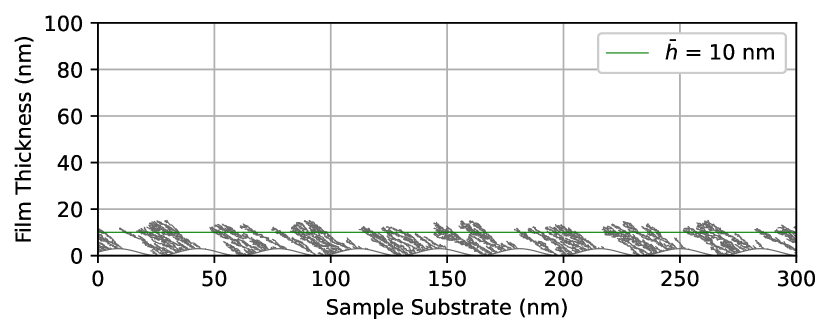
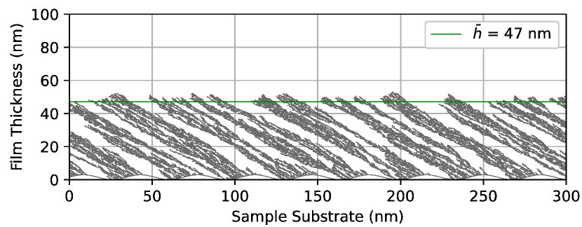
In the case of oblique angle deposition (OAD) at 77°, the reported preferential growth of nanorods on the more exposed areas of ripples that are facing the depositing flux is observed. This preferential growth is shown in Figure 9-(c). The nanorods further grow to form anisotropic tilted columns. When the height of thin-film reaches about 7–10 , they start growing over the adjacent peaks of the substrate. This results in the closure of gaps between the more exposed faces of the rippled substrate. With this, the replicability reduces rapidly and vanishes at about 47 as shown in Figure 9-(d). Keller et al. [10] predicted the angle of growth from tangent rule [27] to be 71° for an angle of deposition 77°. In their experiment, they found a lesser angle of growth and is 50°. The angle of growth obtained in the present simulations is °, which is a better match with the experimental result. This shows that 2D-BD simulations can predict the angle of growth better than the conventional empirical rules. The reported long-lasting growth mode on the more exposed faces of the ripples is also observed in the present simulations.
4 Conclusion
A two-dimensional ballistic deposition code, “2D-BD” based on geometric shadowing effect has been developed to to study the growth of porous nano-structured thin-films. A criterion for the applicability of 2D-BD simulations has been developed. The code is validated by comparing with the published results for a plane substrate and then it is further validated by applying it to two experiments carried out using a plane substrate with a collimator and a sinusoidal patterned substrate. For plane substrate, morphological features such as the angle of growth (), porosity (P) and surface roughness () are studied as functions of the angle of deposition () and the size of the particles. It is found that , P, increase with the increase in the angle of deposition as reported by the earlier studies. The angle of growth () remains constant with the change in size, whereas the porosity and surface roughness increase with the increase in the size of the particle.
For a substrate with a parallel collimator, various morphological features of the deposited films ranging from continuous thin-film to small individual nano-islands are reproduced. The average sizes of nanostructures and the average spacing between them from 2D-BD simulations show a good match with the results obtained in the C-GLAD experiment. The linear density of number of nano-islands obtained in 2D-BD simulations for the spots 3–5 are within the range of the values obtained in the C-GLAD experiment. For a sinusoidal patterned substrate, the reported replicability of the substrate topography by the surface of the thin-film is reproduced up to a height of 120 under normal deposition. In case of oblique angle deposition with the sinusoidal substrate, this replicability reduces rapidly and vanishes by a height of 47 . The experimentally reported preferential and long-lasting growth mode of depositing flux on to the more exposed areas of a rippled substrate is ascertained.The 2D-BD simulations can predict the angle of growth of deposits on patterned substrate better than the conventionally used empirical rules.
2D-BD simulations, though not as exact as MD simulations, are relatively fast and can handle larger sizes of thin-film deposits. They can be used to study the details of experimentally observable morphological features such as the angle of growth, porosity, RMS surface roughness on both the plane and patterned substrates for the thin-films of heights of a few hundred nanometres deposited over a micron sized substrate.
References
References
- [1] W. R. Grove, On the electro-chemical polarity of gases, Philosophical Transactions of the Royal Society of London (142) (1852) 87–101.
- [2] M. Faraday, X. The Bakerian Lecture - Experimental relations of gold (and other metals) to light, Philosophical Transactions of the Royal Society of London (147) (1857) 145–181.
- [3] M. M. Hawkeye, M. T. Taschuk, M. J. Brett, Glancing angle deposition of thin films: Engineering the nanoscale, John Wiley & Sons, 2014.
- [4] N. Nikitenkov, Modern Technologies for Creating the Thin-film Systems and Coatings, BoD–Books on Demand, 2017.
- [5] A. Lakhtakia, R. Messier, Sculptured thin films: Nanoengineered morphology and optics, Vol. 143, SPIE press, 2005.
- [6] D. M. Mattox, V. Mattox, Vacuum coating technology, Springer, 2003.
- [7] P. M. Martin, Handbook of deposition technologies for films and coatings: Science, applications and technology, 3rd Edition, William Andrew, 2010.
- [8] Y. Zhao, D. Ye, G.-C. Wang, T.-M. Lu, Designing nanostructures by glancing angle deposition, in: Nanotubes and Nanowires, Vol. 5219, International Society for Optics and Photonics, 2003, pp. 59–73.
- [9] S. M. Haque, R. De, A. Mitra, J. Misal, C. Prathap, P. V. Satyam, K. D. Rao, Demonstration of tunable Ag morphology from nanocolumns to discrete nanoislands using novel angle constrained glancing angle EB evaporation technique, Surface and Coatings Technology 375 (2019) 363–369.
- [10] A. Keller, L. Peverini, J. Grenzer, G. J. Kovacs, A. Mücklich, S. Facsko, Polycrystalline ni thin films on nanopatterned si substrates: From highly conformal to nonconformal anisotropic growth, Physical Review B 84 (3) (2011) 035423.
- [11] A. Barranco, A. Borras, A. R. Gonzalez-Elipe, A. Palmero, Perspectives on oblique angle deposition of thin films: From fundamentals to devices, Progress in Materials Science 76 (2016) 59–153.
- [12] D. Henderson, M. Brodsky, P. Chaudhari, Simulation of structural anisotropy and void formation in amorphous thin films, Applied Physics Letters 25 (11) (1974) 641–643.
- [13] A. Dirks, H. Leamy, Columnar microstructure in vapor-deposited thin films, Thin solid films 47 (3) (1977) 219–233.
- [14] T. Karabacak, Thin-film growth dynamics with shadowing and re-emission effects, Journal of Nanophotonics 5 (1) (2011) 052501.
- [15] S. Kim, J. Henderson, P. Chaudhari, Computer simulation of amorphous thin films of hard spheres, Thin Solid Films 47 (2) (1977) 155–158.
- [16] R. Jones, C. Standley, L. Maissel, Re-emission coefficients of and films deposited through rf and dc sputtering, Journal of Applied Physics 38 (12) (1967) 4656–4662.
- [17] J. T. Drotar, Y.-P. Zhao, T.-M. Lu, G.-C. Wang, Mechanisms for plasma and reactive ion etch-front roughening, Physical Review B 61 (4) (2000) 3012.
- [18] J. T. Drotar, Y.-P. Zhao, T.-M. Lu, G.-C. Wang, Surface roughening in shadowing growth and etching in 2+ 1 dimensions, Physical Review B 62 (3) (2000) 2118.
- [19] P. Meakin, Ballistic deposition onto inclined surfaces, Physical Review A 38 (2) (1988) 994.
- [20] P. Meakin, Fractals, scaling and growth far from equilibrium, Vol. 5, Cambridge university press, 1998.
- [21] A. Garcia-Valenzuela, R. Álvarez, V. Rico, J. Cotrino, A. R. Gonzalez-Elipe, A. Palmero, Growth of nanocolumnar porous thin films by magnetron sputtering using particle collimators, Surface and Coatings Technology 343 (2018) 172–177.
- [22] G. Troncoso, J. M. García-Martín, M. González, C. Morales, M. Fernández-Castro, J. Soler-Morala, L. Galán, L. Soriano, Silver nanopillar coatings grown by glancing angle magnetron sputtering for reducing multipactor effect in spacecrafts, Applied Surface Science (2020) 146699.
- [23] S. M. Haque, K. D. Rao, S. Tripathi, R. De, D. Shinde, J. Misal, C. Prathap, M. Kumar, T. Som, U. Deshpande, N. Sahoo, Glancing angle deposition of thin films using a novel collimated magnetron sputtering technique, Surface and Coatings Technology 319 (2017) 61–69.
- [24] P. Meakin, R. Jullien, Invited paper, Simple ballistic deposition models for the formation of thin films, in: Modeling of Optical Thin Films, Vol. 821, International Society for Optics and Photonics, 1988, pp. 45–55.
- [25] T. Mansour, R. Rastegar, A. Roitershtein, On ballistic deposition process on a strip, Journal of statistical physics 177 (4) (2019) 626–650.
- [26] Online protractor, https://www.ginifab.com/feeds/angle_measurement/, last Accessed: 10 April, 2021.
- [27] J. Nieuwenhuizen, H. Haanstra, Microfractography of thin films, Philips Tech Rev 27 (3) (1966) 87–91.
- [28] R. Tait, T. Smy, M. Brett, Modelling and characterization of columnar growth in evaporated films, Thin Solid Films 226 (2) (1993) 196–201.
- [29] Y. Zhao, Y. He, C. Brown, Composition dependent nanocolumn tilting angle during the oblique angle co-deposition, Applied Physics Letters 100 (3) (2012) 033106.
- [30] H. Zhu, W. Cao, G. K. Larsen, R. Toole, Y. Zhao, Tilting angle of nanocolumnar films fabricated by oblique angle deposition, Journal of Vacuum Science & Technology B, Nanotechnology and Microelectronics: Materials, Processing, Measurement, and Phenomena 30 (3) (2012) 030606.
- [31] G. G. Lola, J. Parra-Barranco, J. R. Sánchez-Valencia, A. Barranco, A. Borrás, A. R. González-Elipe, M. C. García-Gutiérrez, J. J. Hernández, D. R. Rueda, T. A. Ezquerra, Correlation lengths, porosity and water adsorption in thin films prepared by glancing angle deposition, Nanotechnology 23 (20) (2012) 205701.
- [32] R. Alvarez, L. González-García, P. Romero-Gómez, V. Rico, J. Cotrino, A. R. González-Elipe, A. Palmero, Theoretical and experimental characterization of thin films deposited at oblique angles, Journal of Physics D: Applied Physics 44 (38) (2011) 385302.
- [33] A. W. Sood, D. J. Poxson, F. W. Mont, S. Chhajed, J. Cho, E. F. Schubert, R. E. Welser, N. K. Dhar, A. K. Sood, Experimental and theoretical study of the optical and electrical properties of nanostructured indium tin oxide fabricated by oblique-angle deposition, Journal of nanoscience and nanotechnology 12 (5) (2012) 3950–3953.
- [34] B. C. Hubartt, X. Liu, J. G. Amar, Large-scale molecular dynamics simulations of glancing angle deposition, Journal of Applied Physics 114 (8) (2013) 083517.
- [35] T. Ott, G. Gerlach, Morphological characterization and porosity profiles of tantalum glancing-angle-deposited thin films, Journal of Sensors and Sensor Systems 9 (1) (2020) 79–87.
- [36] P. Meakin, R. Jullien, Restructuring effects in the rain model for random deposition, journal de Physique 48 (10) (1987) 1651–1662.
- [37] J. Krug, P. Meakin, Microstructure and surface scaling in ballistic deposition at oblique incidence, Physical Review A 40 (4) (1989) 2064.
- [38] R. Tait, T. Smy, M. Brett, A ballistic deposition model for films evaporated over topography, Thin Solid Films 187 (2) (1990) 375–384.
- [39] K. Banerjee, J. Shamanna, S. Ray, Surface morphology of a modified ballistic deposition model, Physical Review E 90 (2) (2014) 022111.
- [40] B. Mal, S. Ray, J. Shamanna, Surface properties and scaling behavior of a generalized ballistic deposition model, Physical Review E 93 (2) (2016) 022121.
- [41] Y. Luo, M. Lin, N. Zhou, H. Huang, C.-T. Tsai, L. Zhou, Molecular dynamics simulation study of the microstructure of a-Si: H thin film grown by oblique-angle deposition, Physica B: Condensed Matter 545 (2018) 80–85.
- [42] B. Bouaouina, C. Mastail, A. Besnard, R. Mareus, F. Nita, A. Michel, G. Abadias, Nanocolumnar tin thin film growth by oblique angle sputter-deposition: Experiments vs. simulations, Materials & Design 160 (2018) 338–349.