High Impedence Titanium Nitride Thin Films Grown by Reactive E-beam Evaporation
Superconducting TiN films grown by directional reactive evaporation
Abstract
We report a novel method of growing strongly-disordered superconducting titanium nitride (TiN) thin films by reactive electron-beam deposition. The normal state sheet resistance and superconducting critical temperature (Tc) can be tuned by controlling the deposition pressure in the range of to . For thick films, the sheet resistance () reaches and , which translates into an estimate for the sheet inductance as large as . Benefiting from the directionality of reactive evaporation, we fabricated RF test devices with micron-sized dimensions using a resist mask and a lift-off process, which would be impossible with sputtering or atomic layer deposition methods. The spectroscopic measurements result in consistent sheet inductance values in two different device geometries and the quality factors ranged from Q = 300-2200. The loss is likely due to the presence of titanium oxynitride(TiNxOy) in the morphological composition of our films. The flexibility of the lift-off process suggest applications of reactively-evaporated TiN for making supporting structures around quantum circuits, such as readout resonators or compact on-chip filters.
I Introduction
High kinetic inductance of disordered superconducting films is a useful asset for device applications, including detectors, amplifiers, resonators, and qubits. Eom et al. (2012); Day et al. (2003); Peltonen et al. (2013); Leduc et al. (2010); Samkharadze et al. (2016); Chang et al. (2013); Hazard et al. (2019) These highly disordered superconducting films usually are compound materials such as titanium nitride (TiN), niobium nitride (NbN), or niobium titanium nitride (NbTiN). The two standard processes for creating highly disordered superconducting thin films are sputtering Driessen et al. (2012); Niepce, Burnett, and Bylander (2019) and atomic layer deposition (ALD) Baturina et al. (2007); Shearrow et al. (2018). However, these methods are generally incompatible with depositing through a resist mask, which would be useful for fabricating devices, especially in a situation where the wafer already contains structures from the previous fabrication step. Here we explore a novel approach which utilizes reactive electron beam (e-beam) evaporation to fabricate TiN thin films. Such a process generates a directional TiN flux for deposition while the substrate is maintained at room temperature. This allows for the patterning of a device with standard e-beam lithography resist masks without additional post deposition fabrication and processing. Our growth technique produces highly disordered films whose sheet inductance values are as high as , which is larger than any reported TiN films grown by other growth methods with similar film thickness. Shearrow et al. (2018); Coumou et al. (2013); Ohya et al. (2013) From morphology and composition analysis, we find the strong disorder of e-beam deposited TiN films may originate from mostly amorphous-phased titanium oxynitride (TiNxOy) with nano-crystalline TiN embedded sparsely through out. This fabrication process may provide a alternative way to produce devices with high kinetic inductance.
II Titanium Nitride Fabrication
Our TiN thin films are deposited by reactive e-beam evaporation on silicon-(100) oriented substrates. The substrates were prepared by sonication in acetone and isopropanol, then blown dry with nitrogen. The devices fabricated for DC transport properties were patterned with a Hall bar geometry created by a physical shadow mask. The devices fabricated for RF measurements were patterned by electron-beam lithography using a MMA-EL13 resist mask.
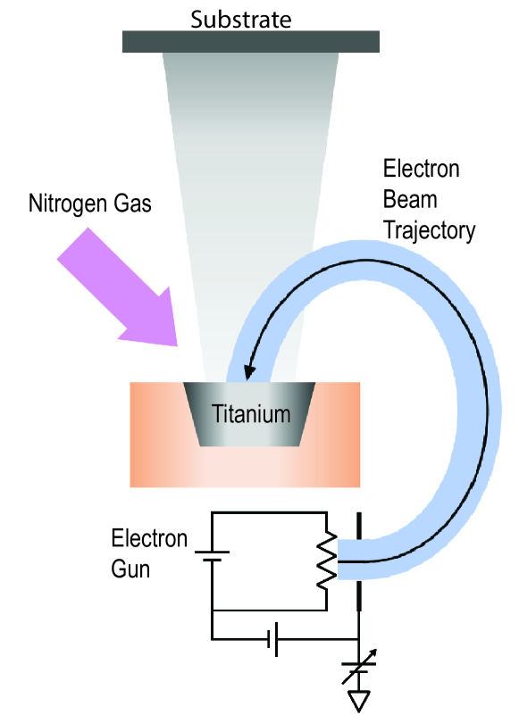
The substrates were then loaded into a Plassys MEB550S E-beam evaporation system where the main deposition scheme is shown in FIG.1. The main deposition chamber is pumped down to a pressure below mbar before beginning the deposition. The deposition procedure started with heating a titanium (with purity 99.995% ) source with the e-beam. Once the titanium evaporation rate stabilized, a controlled flow of ultra-high pure nitrogen gas (with purity 99.999%) was introduced into the deposition chamber. Due to the high energy of the e-beam and the high temperatures of the titanium source, nitrogen gas reacts with the titanium flux to form TiN.
During deposition, the chamber deposition pressure is determined by titanium deposition rate and nitrogen gas flow rate. Clearly, the higher the nitrogen gas flow rate, the higher the chamber pressure. However, the evaporated titanium material can both simultaneously generate titanium flux (raising the chamber pressure) and serve as a titanium sublimation pump (reducing the chamber pressure). To control the chamber pressure and reaction condition, a feedback circuit loop of the e-beam current maintains a constant deposition titanium rate at for all TiN films in this study. The chamber pressure is then tuned by nitrogen flow rate, which is controlled in the range of 0-20 cubic centimeters per minute (sccm) and has a precision of . The actual TiN deposition is only started once both deposition rate and chamber pressures have reached stable values. Unlike ALD growth, the substrate is always maintained at room temperature during the whole deposition process. Also, the evaporated material flux is directional – same as the normal e-beam evaporation process. Thus, this film growth process is suitable for both photo- and e-beam resist mask fabrication techniques. The only required post deposition step of fabricating RF devices is the standard lift-off procedure of the e-beam mask by a heated acetone bath for approximately one hour.
| Sample | (nm) | (mbar) | |||
|---|---|---|---|---|---|
| A | 100 | 52 | 2.65 | 27 | |
| B | 100 | 157 | 2.95 | 73 | |
| C | 100 | 250 | 3.03 | 114 | |
| D | 100 | 316 | 2.95 | 148 | |
| E | 100 | 451 | 2.7 | 231 | |
| F | 100 | 534 | 2.58 | 286 | |
| G | 100 | 600 | 2.35 | 353 | |
| H | 300 | 85 | 3.17 | 37 | |
| I | 200 | 135 | 3.02 | 62 | |
| J | 30 | 855 | 2.4 | 492 | |
| K | 20 | 961 | 1.91 | 674 | |
| L | 10 | 1361 | 0.77 | 2442 |
III DC Transport Measurements
We utilize a physical properties measurement system (PPMS) to characterize DC transport properties of TiN films. All the samples for DC transport are performed by standard four terminal measurements and summarized in Table 1. We found the deposition pressure and film thickness significantly affects the properties of the grown TiN films.
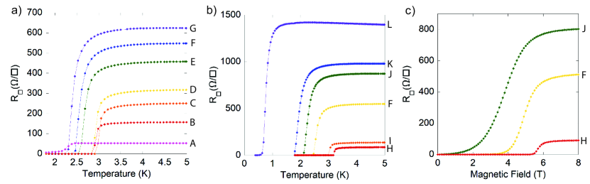
In FIG.2(a), we compare sheet resistance () versus temperature of seven thick films (A through G) grown at deposition pressures, , in a range from to . The normal at increases more than one order of magnitude from to (corresponding to resistivity from to cm, respectively). On the other hand, the first increases but then decreases with increasing . The highest peaked at with the . The non-monotonic behavior of with suggests there is a competition between nitrogen incorporationOhya et al. (2013); Vissers et al. (2013) and suppression of due to disorder.Haviland, Liu, and Goldman (1989); Baturina et al. (2007) According to the Ambegaokar-Baratoff relation and BCS theory, the sheet kinetic inductance can be estimated as .Tinkham (2004) Accordingly, we obtained a wide range of for samples A to G ranging from to .
The TiN film properties are also tunable by changing the film thickness . FIG.2(b) shows versus temperature of six films (sample F and H to L), all grown at the same mbar, with the thicknesses ranging from 10 nm to 300 nm thick. The normal increases with decreasing film thickness. Interestingly, the critical temperature of TiN films decreases with decreasing film thickness. The film shows a critical temperature of while it has the highest normal at . Such behaviors have been observed with strongly disordered superconducting films near thickness tuned superconductor-insulator (SI) transitions.Haviland, Liu, and Goldman (1989); Baturina et al. (2007) With such tunability, the of 10nm TiN film reach up to 2.4nH/, which is nearly one order of magnitude larger than of TiN films grown by sputter and ALD.Coumou et al. (2013); Ohya et al. (2013); Shearrow et al. (2018)
Additionally, the superconductivity of these TiN films can tolerate large perpendicular magnetic fields. FIG.2(c) shows the of sample H, F, J versus perpendicular magnetic fields at . The critical magnetic field for sample H, F, and J are , , and respectively. The critical field is also one to two orders of magnitude larger than the typical aluminum based Josephson junction array devices. This demonstrates disordered TiN films can still serve as a high impedance device in a high magnetic field environment.
IV RF Device and Measurements
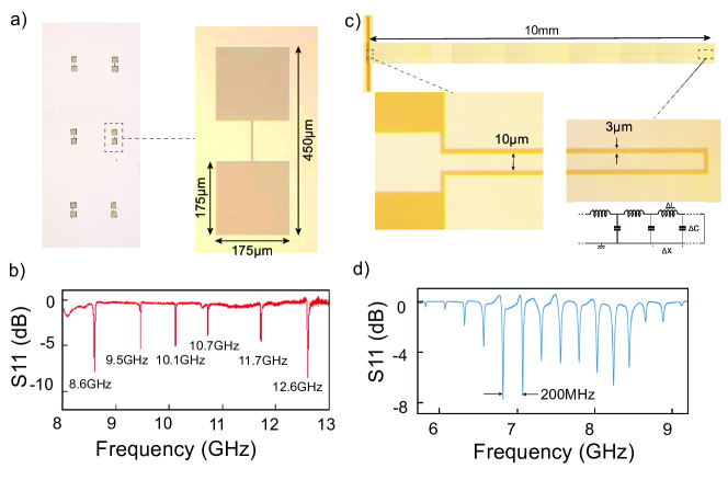
To probe the RF properties of TiN films, we patterned two different types of devices: (1) resonators (shown in FIG.3(a)) and (2) high impedance transmission lines (shown in FIG.3(c)). The measurement utilized the same setup of Kuzmin et al.Kuzmin et al. (2019). The devices are capacitively coupled to a single-port 3D copper waveguide which is then mounted to a dilution refrigerator and the microwave reflection response is probed with a vector network analyzer (VNA).
The resonator device was deposited at mbar with a 100 nm thick TiN film. There were a total of six resonators with a separation of at least to the nearest neighboring resonator such that the coupling between resonators is weak. The capacitance value is dominated by the two square pads. The capacitance of the antenna was determined by HFSS simulations to be 39 fF. The inductance value is dominated by the kinetic inductance of the long thin wire connecting the two pads. The width of the wires are chosen to be , , , , , and for these six different resonators.
The magnitude of the reflected signal, , is shown in FIG3.(b). There are six dips at , , , , , and , which correspond to the resonance frequencies of the six resonators. The total inductance of each resonator can be extrapolated from the measured resonance frequencies and simulated capacitance value. Assuming the inductance values here are all provided by the kinetic inductance of the disordered TiN film, we find the sheet inductance value of each resonator to be , , , , , and . The maximum difference between individual resonator’s sheet inductance is about 4 percent, which reveals the non-uniformity of the TiN film within a single deposition. Moreover, the thickness and deposition pressure of this device is controlled to be the same as film D in the DC measurement experiment but each sample was deposited in two different depositions. The DC measurement analysis of film D revealed a sheet inductance of , which has only a 3 percent difference to the average sheet inductance value of the six resonators in the RF measurement. The systematic difference from deposition to deposition is comparable to sputtering TiN and Josephson junction chains.Ohya et al. (2013); Vissers et al. (2013); Masluk et al. (2012) To extrapolate the intrinsic quality factor (), we used the common expression to fit the reflection coefficient as a function of frequency:Kuzmin et al. (2019)
| (1) |
We obtained values in the range of 1500 - 2200 for the six resonance peaks.
The transmission line device is designed with two parallel 10 mm long, wide TiN wires shown in FIG.3(c). The TiN waveguide was deposited 30 nm thick with . One end of the wire is short circuited and the other end is connected to an antenna which capacitively couples to a 3D copper waveguide.Kuzmin et al. (2019). The magnitude of single-tone reflection signal, S11, as a function of probe frequency is shown in Fig3(d). The S11 reveals resonance dips with equal frequency spacing . The wave-number difference of adjacent modes is defined as , where is the length of the line. In the measured frequency range, we observed a linear dispersion relation, which gives a slow wave velocity . The value of capacitance per micrometer is , which is calculated with a common formula for two coplanar strip lines on top of a silicon substrate.Fouad (1980) Thus, we can obtain the sheet inductance value of TiN for this particular device as . The sheet inductance value is smaller than the value of sample K found via DC measurements. Presumably this is due to a slightly lower TiN deposition pressure of the transmission line device. We also obtained the for each mode with Eq.1. The value of is between - with an average of .
V Morphology and Atomic Composition Characterization
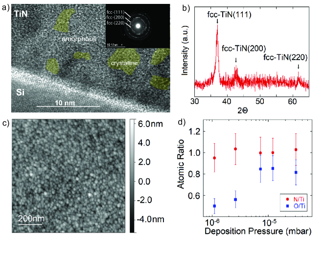
To further understand the origin of the disorder and the morphology in the TiN films, we performed various morphology analysis to the films grown with the same conditions of sample F in Table 1.
First, we used transmission electron microscopy (TEM) to analyze local crystalline morphology of the TiN films. The most striking feature is that most areas are amorphous with only sporadic poly-crystalline embedded within, shown in FIG.4(a). The false color area labeled ’crystalline area’ shows the formation of nano-crystals, which typically have a size less than . The fact that the majority of the films morphology is amorphous, confirms that these TiN films are strongly disordered. The different crystalline orientations seen in TEM is determined with the selected area diffraction (SAD) pattern, shown in the the inlet of the FIG.4(a). The locations of the ring like features indicate that the different crystalline orientation are fcc-TiN (111), fcc-TiN (200), and fcc-TiN (220). Ju et al. (2019) Furthermore, we performed X-ray diffraction (XRD) theta-2 theta analysis to confirm crystalline orientations, shown in FIG.4(b). The peaks found at , , and correspond to fcc-TiN (111), fcc-TiN (200), and fcc-TiN (220), respectively, and are consistent with SAD’s results. Despite the different growth method, the same crystalline orientations have also been found in ALD and sputtered TiN thin films.Shearrow et al. (2018); Vissers et al. (2013); Ohya et al. (2013); Vaz et al. (2002)
We then utilize atomic force microscopy (AFM) to study the surface morphology of the TiN films. FIG.4(c) shows an example of a AFM scan performed on a 100 nm thick TiN film grown at the deposition pressure of sample E. The surface of TiN consists of grains with diameter around . The root mean square surface roughness is while the maximum thickness variation is less than . Therefore, films thinner than may result in physically disconnected structures. To avoid weak links or unwanted vortex structure, the thickness of TiN films should be thicker than while fabricating RF devices.
The atomic composition of the TiN films were analyzed by energy-dispersive X-ray spectroscopy (EDX) with a accelerating voltage variable pressure Hitachi scanning electron microscope. Contrary to the expected composition of just titanium and nitrogen, a large amount of oxygen was present in all TiN films. FIG.4(d) shows a summary of the EDX atomic ratio of nitrogen to titanium (N/Ti) and oxygen to titanium (O/Ti) as a function of deposition pressure. The nitrogen to titanium ratio is nearly 1:1 within the measurement error, which indicates that the nitrogen atom indeed incorporates in the form of titanium nitride. Interestingly, the oxygen to titanium atomic ratio increases from to with an increase in the deposition pressure. During deposition, the partial pressure of oxygen is at least two orders of magnitude lower than nitrogen. Such large amounts of oxygen composition presumably is formed after being exposed to ambient conditions. A similar oxidation process under ambient conditions and the large amounts of oxygen in the chemical composition have also been reported in TiN thin films grown by ALD and sputtering.Shearrow et al. (2018); Ohya et al. (2013) Since SAD and XRD both confirmed that crystalline regimes are formed by TiN, we conclude that the oxygen is diffused into the amorphous regions and form TiNxOy. The large portion of amorphous TiNxOy reveal the origin of the strongly disordered, highly resistive properties and may also explain the low quality factors measured during our RF experiments.
VI Conclusion
In conclusion, the values of the sheet kinetic inductance of TiN films prepared by nitrogen assisted reactive e-beam deposition can be tuned by two orders of magnitude, from to . The tuning knobs are deposition pressure and film thickness. The variations of kinetic inductance within the same deposition and between different depositions is within about 5%. Although the quality factors of our lift-off devices is short of the values accessible with more traditional sputtering or ALD film growth methods, our process can be useful in creating compact high-impedance resonators and filters that survive in a relatively high magnetic fields.
The method for directional reactive TiN deposition was suggested by late Patrick Smuteck to whom this article is dedicated. The authors thank Dr. Sz-Chian Liou from Advance Imaging and Microscopy Lab in University of Maryland for his assistance in TEM imaging and analysis and Dr. Joshua Higgins for assistance with XRD analysis and PPMS measurements. This work was supported by the NSF Career grant (DMR 1455261) and by ARO-LPS program “New and Emerging Qubit Science and Technology” (W911NF1810115).
References
- Eom et al. (2012) B. H. Eom, P. K. Day, H. G. LeDuc, , and J. Zmuidzinas, “A wideband, low-noise superconducting amplifier with high dynamic range,” Nature Physics 8, 623–627 (2012).
- Day et al. (2003) P. K. Day, H. G. LeDuc, B. A. Mazin, A. Vayonakis, and J. Zmuidzinas, “A broadband superconducting detector suitable for use in large arrays,” Nature 425, 817–821 (2003).
- Peltonen et al. (2013) J. T. Peltonen, O. V. Astafiev, Y. P. Korneeva, B. M. Voronov, A. A. Korneev, I. M. Charaev, A. V. Semenov, G. N. Golt’sman, L. B. Ioffe, T. M. Klapwijk, and J. S. Tsai, “Coherent flux tunneling through nbn nanowires,” Phys. Rev. B 88, 220506 (2013).
- Leduc et al. (2010) H. G. Leduc, B. Bumble, P. K. Day, B. H. Eom, J. Gao, S. Golwala, B. A. Mazin, S. McHugh, A. Merrill, D. C. Moore, O. Noroozian, A. D. Turner, and J. Zmuidzinas, “Titanium nitride films for ultrasensitive microresonator detectors,” Applied Physics Letters 97, 102509 (2010).
- Samkharadze et al. (2016) N. Samkharadze, A. Bruno, P. Scarlino, G. Zheng, D. P. DiVincenzo, L. DiCarlo, and L. M. K. Vandersypen, “High-kinetic-inductance superconducting nanowire resonators for circuit qed in a magnetic field,” Phys. Rev. Applied 5, 044004 (2016).
- Chang et al. (2013) J. B. Chang, M. R. Vissers, A. D. Córcoles, M. Sandberg, J. Gao, D. W. Abraham, J. M. Chow, J. M. Gambetta, M. Beth Rothwell, G. A. Keefe, M. Steffen, and D. P. Pappas, “Improved superconducting qubit coherence using titanium nitride,” Applied Physics Letters 103, 012602 (2013).
- Hazard et al. (2019) T. M. Hazard, A. Gyenis, A. Di Paolo, A. T. Asfaw, S. A. Lyon, A. Blais, and A. A. Houck, “Nanowire superinductance fluxonium qubit,” Phys. Rev. Lett. 122, 010504 (2019).
- Driessen et al. (2012) E. F. C. Driessen, P. C. J. J. Coumou, R. R. Tromp, P. J. de Visser, and T. M. Klapwijk, “Strongly disordered tin and nbtin -wave superconductors probed by microwave electrodynamics,” Phys. Rev. Lett. 109, 107003 (2012).
- Niepce, Burnett, and Bylander (2019) D. Niepce, J. Burnett, and J. Bylander, “High kinetic inductance nanowire superinductors,” Phys. Rev. Applied 11, 044014 (2019).
- Baturina et al. (2007) T. I. Baturina, A. Y. Mironov, V. M. Vinokur, M. R. Baklanov, and C. Strunk, “Localized superconductivity in the quantum-critical region of the disorder-driven superconductor-insulator transition in tin thin films,” Phys. Rev. Lett. 99, 257003 (2007).
- Shearrow et al. (2018) A. Shearrow, G. Koolstra, S. J. Whiteley, N. Earnest, P. S. Barry, F. J. Heremans, D. D. Awschalom, E. Shirokoff, and D. I. Schuster, “Atomic layer deposition of titanium nitride for quantum circuits,” Applied Physics Letters 113, 212601 (2018).
- Coumou et al. (2013) P. C. J. J. Coumou, M. R. Zuiddam, E. F. C. Driessen, P. J. de Visser, J. J. A. Baselmans, and T. M. Klapwijk, “Microwave properties of superconducting atomic-layer deposited tin films,” IEEE Transactions on Applied Superconductivity 23, 7500404–7500404 (2013).
- Ohya et al. (2013) S. Ohya, B. Chiaro, A. Megrant, C. Neill, R. Barends, Y. Chen, J. Kelly, D. Low, J. Mutus, P. J. J. O’Malley, P. Roushan, D. Sank, A. Vainsencher, J. Wenner, T. C. White, Y. Yin, B. D. Schultz, C. J. Palmstrøm, B. A. Mazin, A. N. Cleland, and J. M. Martinis, “Room temperature deposition of sputtered TiN films for superconducting coplanar waveguide resonators,” Superconductor Science and Technology 27, 015009 (2013).
- Vissers et al. (2013) M. R. Vissers, J. Gao, J. S. Kline, M. Sandberg, M. P. Weides, D. S. Wisbey, and D. P. Pappas, “Characterization and in-situ monitoring of sub-stoichiometric adjustable superconducting critical temperature titanium nitride growth,” Thin Solid Films 548, 485 – 488 (2013).
- Haviland, Liu, and Goldman (1989) D. B. Haviland, Y. Liu, and A. M. Goldman, “Onset of superconductivity in the two-dimensional limit,” Phys. Rev. Lett. 62, 2180–2183 (1989).
- Tinkham (2004) M. Tinkham, Introduction to Superconductivity, 2nd ed. (Dover Publications, 2004).
- Kuzmin et al. (2019) R. Kuzmin, R. Mencia, N. Grabon, N. Mehta, Y.-H. Lin, and V. E. Manucharyan, “Quantum electrodynamics of a superconductor–insulator phase transition,” Nature Physics 15, 930–934 (2019).
- Masluk et al. (2012) N. A. Masluk, I. M. Pop, A. Kamal, Z. K. Minev, and M. H. Devoret, “Microwave characterization of josephson junction arrays: Implementing a low loss superinductance,” Phys. Rev. Lett. 109, 137002 (2012).
- Fouad (1980) V. H. Fouad, “Finite boundary corrections to oplanar stripline analysis,” Electronics Letters 16, 604 (1980).
- Ju et al. (2019) H. Ju, N. Ding, J. Xu, L. Yu, Y. Geng, F. Ahmed, B. Zuo, and L. Shao, “The influence of crystal structure and the enhancement of mechanical and frictional properties of titanium nitride film by addition of ruthenium,” Applied Surface Science 489, 247 – 254 (2019).
- Vaz et al. (2002) F. Vaz, P. Machado, L. Rebouta, J. Mendes, S. Lanceros-Méndez, L. Cunha, S. Nascimento, P. Goudeau, J. Rivière, E. Alves, and A. Sidor, “Physical and morphological characterization of reactively magnetron sputtered tin films,” Thin Solid Films 420-421, 421 – 428 (2002).
- Sandberg et al. (2012) M. Sandberg, M. R. Vissers, J. S. Kline, M. Weides, J. Gao, D. S. Wisbey, and D. P. Pappas, “Etch induced microwave losses in titanium nitride superconducting resonators,” Applied Physics Letters 100, 262605 (2012).