Indirect-to-direct band gap crossover of single walled MoS2 nanotubes
Abstract
Using density functional theory, the electronic structures of single walled molybdenum disulfide nanotubes (MoS2 NTs) were investigated as a function of diameter. Our calculations show that the electronic structure near the band gap is sensitive to the NT diameter: armchair MoS2 NTs act as indirect gap semiconductors for diameters up to approximately 5.0 nm, while armchair MoS2 NTs with larger diameters act as direct gap semiconductors with band edges located in the vicinity of . This finding implies that MoS2 NTs with large diameters should exhibit similar photoluminescence to 2D monolayer MoS2 sheets. This indirect-to-direct band gap crossover is ascribed to the upward shift of the valence band peak at the point in small diameter NTs, which is caused by the tensile strain resulting from their tubular structures.
Since the discovery of graphene, atomic layer materials have attracted much attention due to their unique physical properties arising from chemically inert 2D covalent networks with an unusual network topology. The constituent elements and network structure provide these materials with a variety of properties, ranging from metals to insulators. Transition metal dichalcogenides (TMDCs), such as MoS2, WS2, WSe2, and MoTe2, are representative examples of such atomic layer materials. TMDCs consist of an atomic layer of transition metals that form a triangular lattice sandwiched by atomic layers of chalcogens arranged in a prismatic manner, resulting in a hexagonal network of these elements with a thickness of approximately 0.3 nm Friend and Yoffe (1987); Wang et al. (2012). According to the chemical valence of the constituent elements in TMDCs, monolayers of TMDCs are primarily semiconductors, with a direct band gap at the K point Roldán et al. (2014); Mak et al. (2010); Splendiani et al. (2010), which strongly depends on the constituent elements; in contrast, corresponding thin films or bulk materials are indirect band gap semi-conductors.
Due to the chemical stability of these 2D lattices with covalent bonds, TMDCs have been employed as starting materials to construct various derivatives. Such derivatives can provide building blocks of various layered heterostructures, where each layer is bound via weak van der Waals interactions Geim and Grigorieva (2013); Novoselov et al. (2016); Liu et al. (2016). In these van der Waals heterostructures, one can tune the electronic structure near the band edges by assembling and stacking them in an appropriate manner, leading to the potential for optical and electronic applications Lee et al. (2014); Zhang et al. (2016). Nanoribbons provide another possible derivative, obtained by imposing an open boundary condition on TMDC sheets. The formation energy and electronic structures of TMDC nanoribbons are strongly dependent on the edge morphology Li et al. (2008); Ataca et al. (2011), due to the polarity at the edges and structural relaxation. In addition to nanoribbons, nanotubes (NTs) of TMDCs Tenne et al. (1992); Tenne and Redlich (2010) are also available, by imposing a tubular boundary condition on nanoribbons. Indeed, researchers recently reported the synthesis of single walled MoS2 NT wrapping walls of multi-walled boron nitride NTs Xiang et al. (2020). The authors reported photoluminescence (PL) from these single walled MoS2 NTs, with a similar energy to the 2D monolayer MoS2. This behavior implies that the electronic properties of single walled MoS2 NT act as a direct band gap semiconductor, even with the tubular structure.
Prior to the experimental synthesis of single walled MoS2 NTs, their electronic properties were intensively studied Seifert et al. (2000); Zhang, Dumitricǎ, and Seifert (2010); Zibouche, Kuc, and Heine (2012). It has been reported that these NTs have intrinsic semiconducting electronic structures because their 2D counterpart is a semiconductor with a direct band gap at the K point Mak et al. (2010); Splendiani et al. (2010). It has also been revealed that the band edge structure depends on the NT chirality. Zigzag (,0) NTs have direct band gaps at the point, while armchair (,) and chiral NTs have indirect band gaps between the vicinity of the point and the middle of the 1D Brillouin zone (BZ) for the valence and conduction band edges, respectively. These theoretical insights into the electronic band structure of single-walled MoS2 NTs are not fully accountable for the recent experimental finding that MoS2 NTs have a direct band gap causing PL. In addition, the results also imply the existence of a missing link that connects the indirect band gap of the tubular form and the direct band gap of the planar form of MoS2.
In this report, we aim to determine the critical NT diameter at which the indirect-to-direct band gap crossover occurs in order to connect the discontinuity between the indirect gaps of NTs and the direct gap of sheets. Using density functional theory (DFT) Hohenberg and Kohn (1964); Kohn and Sham (1965), we investigated the electronic structures of armchair MoS2 NTs, with diameters ranging from 1.6 to 6.8 nm. The DFT calculations revealed that MoS2 NTs with diameters larger than 5.2 nm are semiconductors with an indirect band gap in the vicinity of , corresponding to the valence and conduction band valleys at the K point of an isolated MoS2 sheet. Furthermore, our structural analysis of MoS2 NTs demonstrated that the curvature-induced mechanical strain causes the indirect band gaps of MoS2 NTs with small diameters.
All of the calculations in this study were performed using DFT implemented in the Simulation Tool for Atom Technology (STATE) program package Morikawa, Iwata, and Terakura (2001). The general gradient approximation (GGA) was applied with the Perdew–Burke–Ernzerhof functional Perdew, Burke, and Ernzerhof (1996, 1997) to describe the exchange correlation potential energy among interacting electrons. The ultrasoft pseudopotential generated by the Vanderbilt scheme Vanderbilt (1990) was used to provide the interaction between valence electrons and nuclei. The valence wave functions and deficit charge density were expanded in terms of the plane wave basis set, with cutoff energies of 340 and 3061 eV (25 and 225 Ry), respectively.
In this work, we considered armchair MoS2 NTs with diameters ranging from 1.6 to 6.8 nm, which correspond to the indices (9,9) and (39,39), to determine the critical diameter at which the band gap crossover occurs. To exclude the effect arising from inter-tube periodic boundary conditions normal to the NT, the NTs were separated from their periodic images by 0.9 nm vacuum spacing. BZ integration was conducted under six equidistant k points along the tube axis. The atomic coordinates were optimized using a fixed lattice parameter of 0.315 nm, corresponding to the experimental value for planar MoS2 Wakabayashi, Smith, and Nicklow (1975), until the forces acting on each atom were less than 0.684 eV/nm (1.3310-3 Hartree/au).
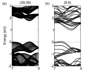
Figure 1 shows the electronic structure of the MoS2 NTs, from the point () to the X point () in the Brillouin zone. The band dispersion relation was sensitive to the tube diameter, even though these NTs had the same armchair chirality. The (39,39) MoS2 NT was a direct band gap semiconductor, with the valence and conduction band edges located in the vicinity of [Fig. 1(a)], corresponding to the K point of the 2D BZ. This result indicates that the band edge positions of the NTs with large diameters originate from the valleys of the isolated MoS2 sheet, confirming the expectation that the electronic band structure near the gap of the NTs should asymptotically approach that of an isolated MoS2 sheet. In contrast to the (39,39) NT, the (9,9) NT had an indirect band gap between near and for the valence and conduction band edges, respectively [Fig. 1(b)], as observed in the previous calculations. Thus, NTs with a large diameter should exhibit PL, as observed for isolated sheets of MoS2.
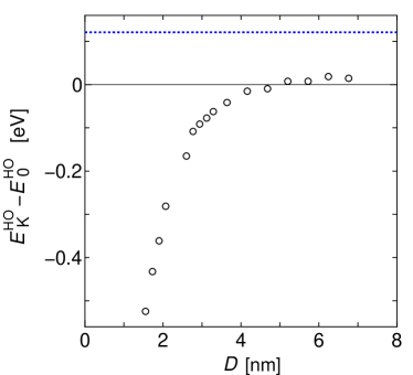
To determine the critical diameter at which the indirect-to-direct band gap crossover occurs, we investigated the energy difference between the peak of the highest energy of the occupied state in valence band at near , , and at , corresponding to the K point of 2D, . Figure 2 shows the energy difference, as a function of NT diameter, . The energy difference, monotonically increases with increasing diameter, crossing zero at a diameter of approximately 5.0 nm. Therefore, the NTs with a diameter of 5.0 nm or larger have a direct band gap in the vicinity of and are expected to exhibit PL at the band gap energy. Note that the asymptotic property of the energy peak difference rises extremely slowly with increasing diameter. The peak difference for the NT with the largest diameter is still smaller (by 0.1 eV) than that of the monolayer MoS2 sheet.
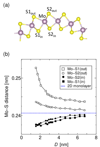
The diameter dependence of the valence band edge of the MoS2 NTs indicates that the effect of the structural strain arises from the curvature. Figure 3 shows the bond length between Mo and S atoms as a function of tube diameter. The tubular structure and symmetry result in four distinct Mo-S distances. Two of the four distances, corresponding to outer Mo-S bonds, increase with decreasing diameter, while the other two distances, corresponding to inner Mo-S bonds, decrease with decreasing diameter. The bond deformations of the outer Mo-S bonds are larger than those of the inner Mo-S bonds. In particular, the outer Mo-S bond perpendicular to the tube axis is elongated by a factor of four compared with that of the inner Mo-S bonds. Therefore, the atoms in the MoS2 NTs are subjected to tensile and compressive strain in the outer and inner regions, respectively. Furthermore, the tensile strain for the outer part is dominant for the structural distortion. This structural deformation can account for the diameter-dependent edge modulation observed for the valence band of the MoS2 NT because the valence band edge of monolayer MoS2 is sensitive to strain Conley et al. (2013); Gong et al. (2013); Ghorbani-Asl et al. (2013).
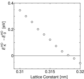
To confirm the effect of strain on the electronic structure of MoS2 sheets, we investigated the electronic structure of isolated MoS2 sheets. Figure 4 shows the energy difference between the K and points of the highest branch of the valence band as a function of the lattice parameter. With increasing lattice parameter, which corresponds to the tensile strain, the energy difference decreased and crossed zero at a tensile strain of 1.84%, with an Mo-S distance of 0.318 nm. Therefore, the tensile strain caused the upward shift of the peak at the point, leading to the indirect band gap structure for the MoS2 sheet. This upward shift is associated with the wave function distribution of the valence band top at the point, where the state consists of the state of Mo and the state of S atoms with a bonding nature Gong et al. (2013). Therefore, the state was shifted upward by the tensile strain, which reduced the orbital hybridization. This analysis clearly confirms that the band gap crossover in MoS2 NTs is induced by the strain associated with their curvature.
Based on DFT with GGA, we investigated the electronic structure of armchair MoS2 NTs with diameters of 1.6-6.8 nm. Our DFT calculations showed that NTs with diameters of up to 5.0 nm are semiconductors with an indirect band gap, whereas NTs with diameters of 5.0 nm or larger have a direct band gap between valleys in the vicinity of , corresponding to the band edge valleys of monolayer MoS2. The results confirm that the electronic structure of MoS2 exhibits asymptotical properties transitioning from an indirect to a direct band gap based on the diameter. Therefore, MoS2 NTs with diameters of 5.2 nm or larger may exhibit PL, as observed for monolayer MoS2 sheets, and may represent a constituent material for designing optical, optoelectronic, and valleytronic devices. Structural analysis of the MoS2 NTs revealed that the tensile strain on the outer part of the NTs caused an upward shift of the valence band peak near the point, leading to the indirect-to-direct band gap crossover associated with the NT diameter.
Part of this work was financially supported by JSPS KAKENHI Grant Numbers JP17K06187, JP18H05329, JP19J13818 and JP20H00220. Some of the calculations were performed on NEC SX-Ace at the Cybermedia Center in Osaka University and on Oakbridge-CX at Information Technology center in the University of Tokyo.
References
- Friend and Yoffe (1987) R. Friend and A. Yoffe, “Electronic properties of intercalation complexes of the transition metal dichalcogenides,” Adv. Phys. 36, 1–94 (1987).
- Wang et al. (2012) Q. H. Wang, K. Kalantar-Zadeh, A. Kis, J. N. Coleman, and M. S. Strano, “Electronics and optoelectronics of two-dimensional transition metal dichalcogenides,” Nat. Nanotechnol. 7, 699–712 (2012).
- Roldán et al. (2014) R. Roldán, J. A. Silva-Guillén, M. P. López-Sancho, F. Guinea, E. Cappelluti, and P. Ordejón, “Electronic properties of single-layer and multilayer transition metal dichalcogenides MX2 (M = Mo, W and X = S, Se),” Ann. Phys. 526, 347–357 (2014), 1410.2154 .
- Mak et al. (2010) K. F. Mak, C. Lee, J. Hone, J. Shan, and T. F. Heinz, “Atomically thin MoS2: A new direct-gap semiconductor,” Phys. Rev. Lett. 105, 136805 (2010), 1004.0546 .
- Splendiani et al. (2010) A. Splendiani, L. Sun, Y. Zhang, T. Li, J. Kim, C. Y. Chim, G. Galli, and F. Wang, “Emerging photoluminescence in monolayer MoS2,” Nano Lett. 10, 1271–1275 (2010).
- Geim and Grigorieva (2013) A. K. Geim and I. V. Grigorieva, “Van der Waals heterostructures,” Nature 499, 419–425 (2013), 1307.6718 .
- Novoselov et al. (2016) K. S. Novoselov, A. Mishchenko, A. Carvalho, and A. H. Castro Neto, “2D materials and van der Waals heterostructures,” Science 353, aac9439 (2016).
- Liu et al. (2016) Y. Liu, N. O. Weiss, X. Duan, H.-C. Cheng, Y. Huang, and X. Duan, “Van der Waals heterostructures and devices,” Nat. Rev. Mater 1, 16042 (2016).
- Lee et al. (2014) C. H. Lee, G. H. Lee, A. M. Van Der Zande, W. Chen, Y. Li, M. Han, X. Cui, G. Arefe, C. Nuckolls, T. F. Heinz, J. Guo, J. Hone, and P. Kim, “Atomically thin p-n junctions with van der Waals heterointerfaces,” Nat. Nanotechnol. 9, 676–681 (2014).
- Zhang et al. (2016) K. Zhang, T. Zhang, G. Cheng, T. Li, S. Wang, W. Wei, X. Zhou, W. Yu, Y. Sun, P. Wang, D. Zhang, C. Zeng, X. Wang, W. Hu, H. J. Fan, G. Shen, X. Chen, X. Duan, K. Chang, and N. Dai, “Interlayer Transition and Infrared Photodetection in Atomically Thin Type-II MoTe2/MoS2 van der Waals Heterostructures,” ACS Nano 10, 3852–3858 (2016).
- Li et al. (2008) Y. Li, Z. Zhou, S. Zhang, and Z. Chen, “MoS2 nanoribbons: High stability and unusual electronic and magnetic properties,” J. Am. Chem. Soc. 130, 16739–16744 (2008).
- Ataca et al. (2011) C. Ataca, H. Şahin, E. Aktuörk, and S. Ciraci, “Mechanical and electronic properties of MoS2 nanoribbons and their defects,” J. Phys. Chem. C 115, 3934–3941 (2011).
- Tenne et al. (1992) R. Tenne, L. Margulis, M. Genut, and G. Hodes, “Polyhedral and cylindrical structures of tungsten disulphide,” Nature 360, 444–446 (1992).
- Tenne and Redlich (2010) R. Tenne and M. Redlich, “Recent progress in the research of inorganic fullerene-like nanoparticles and inorganic nanotubes,” Chem. Soc. Rev. 39, 1423–1434 (2010).
- Xiang et al. (2020) R. Xiang, T. Inoue, Y. Zheng, A. Kumamoto, Y. Qian, Y. Sato, M. Liu, D. Tang, D. Gokhale, J. Guo, K. Hisama, S. Yotsumoto, T. Ogamoto, H. Arai, Y. Kobayashi, H. Zhang, B. Hou, A. Anisimov, M. Maruyama, Y. Miyata, S. Okada, S. Chiashi, Y. Li, J. Kong, E. I. Kauppinen, Y. Ikuhara, K. Suenaga, and S. Maruyama, “One-dimensional van der Waals heterostructures,” Science 367, 537–542 (2020), 1807.06154 .
- Seifert et al. (2000) G. Seifert, H. Terrones, M. Terrones, G. Jungnickel, and T. Frauenheim, “Structure and electronic properties of MoS2 nanotubes,” Phys. Rev. Lett. 85, 146–149 (2000).
- Zhang, Dumitricǎ, and Seifert (2010) D. B. Zhang, T. Dumitricǎ, and G. Seifert, “Helical nanotube structures of MoS2 with intrinsic twisting: An objective molecular dynamics study,” Phys. Rev. Lett. 104, 1–4 (2010).
- Zibouche, Kuc, and Heine (2012) N. Zibouche, A. Kuc, and T. Heine, “From layers to nanotubes: Transition metal disulfides TMS2,” Eur. Phys. J. B 85, 1–7 (2012), 1302.3478 .
- Hohenberg and Kohn (1964) P. Hohenberg and W. Kohn, “Inhomogeneous Electron Gas,” Phys. Rev. 136, B864–B871 (1964).
- Kohn and Sham (1965) W. Kohn and L. J. Sham, “Self-Consistent Equations Including Exchange and Correlation Effects,” Phys. Rev. 140, A1133–A1138 (1965).
- Morikawa, Iwata, and Terakura (2001) Y. Morikawa, K. Iwata, and K. Terakura, “Theoretical study of hydrogenation process of formate on clean and Zn deposited Cu(111) surfaces,” Appl. Surf. Sci. 169-170, 11–15 (2001).
- Perdew, Burke, and Ernzerhof (1996) J. Perdew, K. Burke, and M. Ernzerhof, “Generalized Gradient Approximation Made Simple.” Phys. Rev. Lett. 77, 3865–3868 (1996).
- Perdew, Burke, and Ernzerhof (1997) J. P. Perdew, K. Burke, and M. Ernzerhof, “Generalized Gradient Approximation Made Simple (vol 77, pg 3865, 1996),” Phys. Rev. Lett. 78, 1396–1396 (1997), 0927-0256(96)00008 [10.1016] .
- Vanderbilt (1990) D. Vanderbilt, “Soft self-consistent pseudopotentials in a generalized eigenvalue formalism,” Phys. Rev. B 41, 7892–7895 (1990).
- Wakabayashi, Smith, and Nicklow (1975) N. Wakabayashi, H. G. Smith, and R. M. Nicklow, “Lattice dynamics of hexagonal MoS2 studied by neutron scattering,” Phys. Rev. B 12, 659–663 (1975).
- Conley et al. (2013) H. J. Conley, B. Wang, J. I. Ziegler, R. F. Haglund, S. T. Pantelides, and K. I. Bolotin, “Bandgap engineering of strained monolayer and bilayer MoS2,” Nano Lett. 13, 3626–3630 (2013), 1305.3880 .
- Gong et al. (2013) C. Gong, H. Zhang, W. Wang, L. Colombo, R. M. Wallace, and K. Cho, “Band alignment of two-dimensional transition metal dichalcogenides: Application in tunnel field effect transistors,” Appl. Phys. Lett. 103 (2013), 10.1063/1.4817409.
- Ghorbani-Asl et al. (2013) M. Ghorbani-Asl, N. Zibouche, M. Wahiduzzaman, A. F. Oliveira, A. Kuc, and T. Heine, “Electromechanics in MoS2 and WS2: Nanotubes vs. monolayers,” Sci. Rep. 3, 2961 (2013), 1308.1834 .