SupReferences
Scalable graphene platform for Tbits/s data transmission
Abstract
To date, no electro-optic platform enables devices with high bandwidth, small footprint, and low power consumption, while also enabling mass production. Here we demonstrate high-yield fabrication of high-speed graphene electro-absorption modulators using CVD-grown graphene. We minimize variation in device performance from graphene inhomogeneity over large area by engineering graphene-mode overlap and device capacitance to ensure high extinction ratio. We fabricate an 8 mm 1 mm chip with 32 graphene electro-absorption modulators and measure 94% yield with bit error rate below the hard-decision forward error correction limit at 7 Gbits/s, amounting to a total aggregated data rate of 210 Gbits/s. Monte Carlo simulations show that data rates 0.6 Tbits/s are within reach by further optimizing device cross-section, paving the way for graphene-based ultra-high data rate applications.
1 Introduction
With data traffic growing exponentially, there is an urgent demand for optical modulators with large bandwidth, small footprint, and low power consumption, that can be mass-produced [1]. Although integrated graphene modulators offer high bandwidth with small footprint and low energy consumption [2, 3, 4], low device yield has been a major challenge. There have been significant advancements in growing and transferring chemical vapor deposition (CVD) graphene at wafer-scale [5, 6], but these films are inherently polycrystalline and exhibit nonuniformities of conductance and carrier density at the micrometer scale due to grain boundaries and defects [7, 8]. Furthermore, graphene transfer and fabrication steps contribute to nonuniformity by increasing contamination (such as polymer residues) and unwanted doping. While these inhomogeneities are believed to cause large variation in device performance [9, 10, 11], large area analysis for photonic devices have not been shown to date.
Here we demonstrate large yield of high-speed graphene electro-absorption modulators using commercially available CVD polycrystalline graphene. We design the modulator to exhibit high extinction ratio relative to the undesired doping induced extinction, ensuring high optical signal-to-noise ratio (OSNR). We achieve strong extinction ratio modulation by integrating a dual-layer graphene capacitor on a silicon nitride (\chSi3N4) waveguide with alumina (\chAl2O3) gate dielectric for large device capacitance. Moreover, we ensure strong graphene-mode overlap by placing this graphene capacitor directly above the \chSi3N4 waveguide for maximum graphene-mode coupling. We show the schematic of the graphene electro-absorption modulator in Figure 1. Light guided by the waveguide is absorbed by the graphene capacitor.
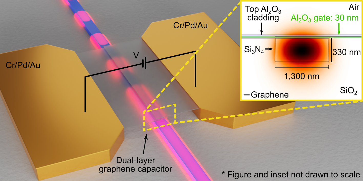
Light guided by the waveguide passes through the modulator and is absorbed by the graphene capacitor. Inset: device cross-section consisting of two graphene sheets (black lines) separated by a 30 nm ALD \chAl2O3 gate dielectric (green layer) and a 330 nm tall \chSi3N4 waveguide. The widths of the waveguide and graphene capacitor are 1.3 µm. We superimpose the simulated fundamental quasi-TE mode of the waveguide with the device structures to show graphene capacitor’s proximity to the mode for strong coupling via evanescent waves. We deposit a 30 nm \chAl2O3 cladding above the top graphene sheet to protect the capacitor.
The capacitor consists of two graphene sheets (black lines in the inset of Figure 1) separated by a 30 nm ALD \chAl2O3 gate dielectric (green layer) to form a parallel plate capacitor. We modulate graphene absorption and propagation loss by applying voltage to the capacitor. This electrostatically gates the two graphene sheets which induces Pauli-blocking and suppresses interband transitions of carriers [12, 13]. As shown in the inset of Figure 1, we maximize the coupling between graphene and the fundamental quasi-TE mode via evanescent waves by placing the capacitor directly above the waveguide.
2 Graphene transmitter chip fabrication
We fabricate an 8 mm 1 mm chip with 32 graphene electro-absorption modulators to characterize variations in modulation depth, bandwidth, and data transmission quality. We outline the fabrication steps for the graphene modulator in Figure 2.
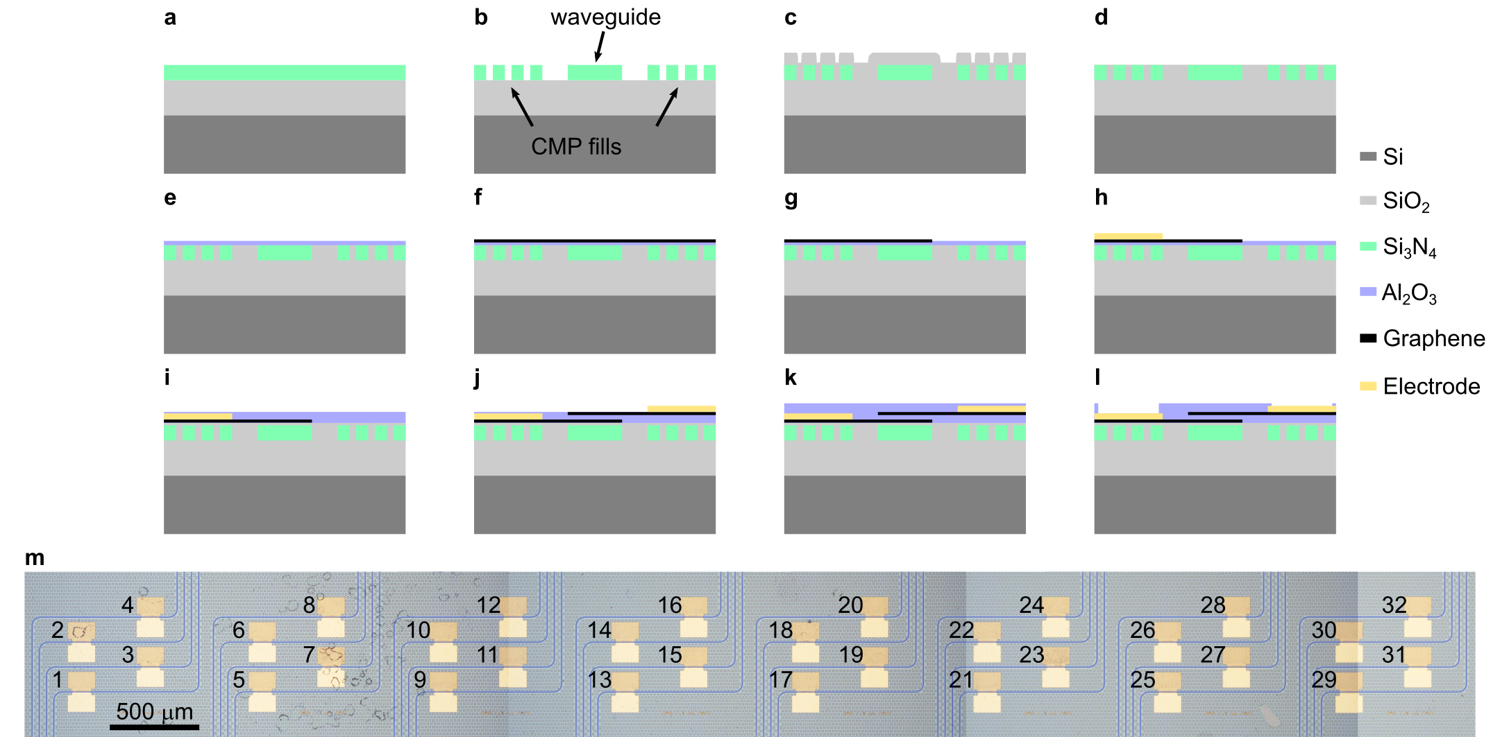
(a) Deposition of 330 nm of LPCVD \chSi3N4 on 4.3 µm-thick thermal \chSiO2 on silicon substrate. (b) Patterning and etching of the waveguides and 10 µm by 10 µm square fills for CMP. (c) Cladding deposition of PECVD \chSiO2. (d) Top cladding removal and planarization of the chip surface with CMP to expose the top of the \chSi3N4 waveguide. (e) Deposition of 10 nm of ALD \chAl2O3. (f) Transferring of CVD graphene on copper foil (Grolltex Inc.) via electrochemical delamination wet transfer (also see Supplementary Information). (g) Etching of the transferred graphene film with \chO2 plasma to form the bottom capacitor plate. (h) Deposition of the electrode (Cr/Pd/Au, 1 nm/45 nm/50 nm) using e-beam evaporation at high vacuum ( Torr). (i) Thermal evaporation of 1 nm of aluminum to serve as a seed layer (after electrode lift-off) for subsequent deposition of 30 nm ALD \chAl2O3 gate dielectric. (j) Transferring and patterning of the second graphene layer similarly to the first one, followed by electrode deposition (steps f-h). (k) Deposition of a final of 30 nm thick ALD \chAl2O3 on top of the second graphene sheet to protect the capacitor. (l) Opening vias with buffered oxide etch (50:1) to remove \chAl2O3 and access the electrodes. (m) Tiled optical micrograph of the 8 mm 1 mm transmitter chip with 32 graphene electro-absorption modulators. The waveguides are false-colored in blue to stand out among CMP fills. Each device consists of a 100 µm long and 1.3 µm wide dual-layer graphene capacitor to modulate waveguide transmission. Therefore, the device’s active area only covers approximately 370 µm2.
We first deposit 330 nm of LPCVD \chSi3N4 on 4.3 µm-thick thermal \chSiO2 on silicon substrate. We then pattern and etch the waveguides and 10 µm by 10 µm square fills for CMP (see Figure 2b). We deposit a cladding layer over the \chSi3N4 patterns with PECVD \chSiO2. We remove the top cladding and planarize the chip with CMP to expose the top surface of the \chSi3N4 waveguide. This planarization step helps prevent damage to the graphene sheets during transfer and ensures that the graphene is in direct contact with the waveguide, maximizing mode overlap. To screen charge impurities on the surface and minimize undesired substrate doping to graphene, we deposit 10 nm of \chAl2O3 via ALD. We transfer CVD graphene on copper foil (Grolltex Inc. [14]) via electrochemical delamination wet transfer. This method enables transfer of large-area films with ease and minimal chemical/mechanical damage to the graphene [15, 16] (see Supplementary Information). We etch the transferred graphene film with \chO2 plasma to form the bottom capacitor plate, followed by deposition of the electrode (Cr/Pd/Au, 1 nm/45 nm/50 nm) using e-beam evaporation at high vacuum ( Torr). After electrode lift-off, we thermally evaporate 1 nm of aluminum to serve as a seed layer for subsequent deposition of 30 nm ALD \chAl2O3 gate dielectric. We transfer and pattern the second graphene layer similarly to the first one, followed by electrode deposition (Figure 2f-h). In order to protect the capacitor, we deposit a final layer of 30 nm thick ALD \chAl2O3 on top of the second graphene sheet. We open vias using buffered oxide etch (50:1) to remove \chAl2O3 and access the electrodes. The fabricated graphene transmitter chip is shown in the tiled optical micrograph in Figure 2m. The waveguides are false-colored in blue to stand out among CMP fills. Each device consists of a 100 µm long and 1.3 µm wide dual-layer graphene capacitor used to modulate waveguide transmission.
3 Experimental Results
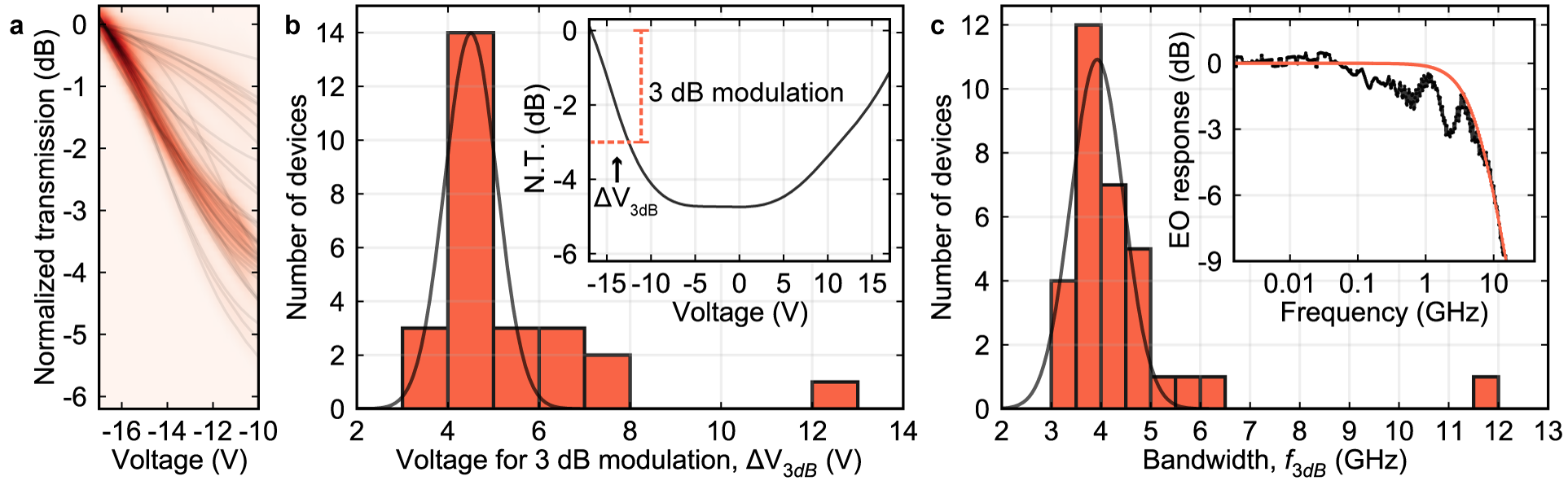
(a) Normalized transmission of 32 modulators as a function of voltage around the operating region (V = –17 V to –10 V). We superimpose the transmission density plot of all modulators (red) over the individual curve of each modulator (gray solid lines). The modulators exhibit similar transmission characteristics, especially around –17 V to –13 V, as shown by the dark and narrow width of the density curve. (b) Histogram of the measured voltage changes required for 3 dB modulation from maximum transmission, V3dB. Inset: example transmission curve describing V3dB. The solid line in the histogram is a normal distribution fit to the data with a standard deviation of 0.57 V ( 13% of the mean 4.50 V). (c) Histogram of the measured modulator bandwidths. The standard deviation is 0.53 GHz ( 14% of the mean 3.92 GHz). Inset: example frequency response curve along with the fit to a single-pole transfer function (solid orange line), where is the frequency and is the modulator time constant.
We show standard deviation of less than 13% for both modulation efficiency (4.5 V for 3 dB modulation) and bandwidth (3.9 GHz) despite the devices exhibiting graphene residual doping variation of more than 30% across the same chip area (8 mm 1 mm, see Figure S5 in the Supplementary Information). We show in Figure 3a the normalized transmission of 32 modulators with respect to voltage around the operating region (V = –17 V to –10 V). We superimpose the transmission density plot of all modulators (red) over the individual curve of each modulator (gray solid lines). The modulators exhibit similar transmission characteristics, especially around –17 V to –13 V, as shown by the dark and narrow width of the density curve. To quantify modulation efficiency, we measure the voltage required for 3 dB modulation from maximum transmission, V3dB, and plot a histogram in Figure 3b (the inset of Figure 3b shows an example transmission curve describing V3dB). We fit a normal distribution to the histogram (black solid line in Figure 3b) and measure a standard deviation of 0.57 V, which is less than 13% of the mean (4.50 V). We also measure the modulators’ bandwidths and plot the histogram in Figure 3c. We measure a standard deviation of 0.5 GHz from the fit, which is about 13% from the mean (3.9 GHz). In the inset of Figure 3c, we show an example of the frequency response curve of one of the modulators. The orange line corresponds to the fit to a single-pole transfer function , where is the frequency and is the modulator time constant.
We measured 94% yield (30 out of 32 devices) with bit error rate (BER) below the hard-decision forward error correction (HD-FEC) limit (BER ) [17] at 7 Gbits/s, amounting to a total aggregated data rate of 210 Gbits/s for the chip. In Figure 4 we show the measured eye diagram of each modulator driven with 2 non-return-to-zero (NRZ) pseudorandom binary sequence (PRBS) at 7 Gbits/s and Vpp = 6 V (the modulator number corresponds to that shown in the tiled optical micrograph in Figure 2b).
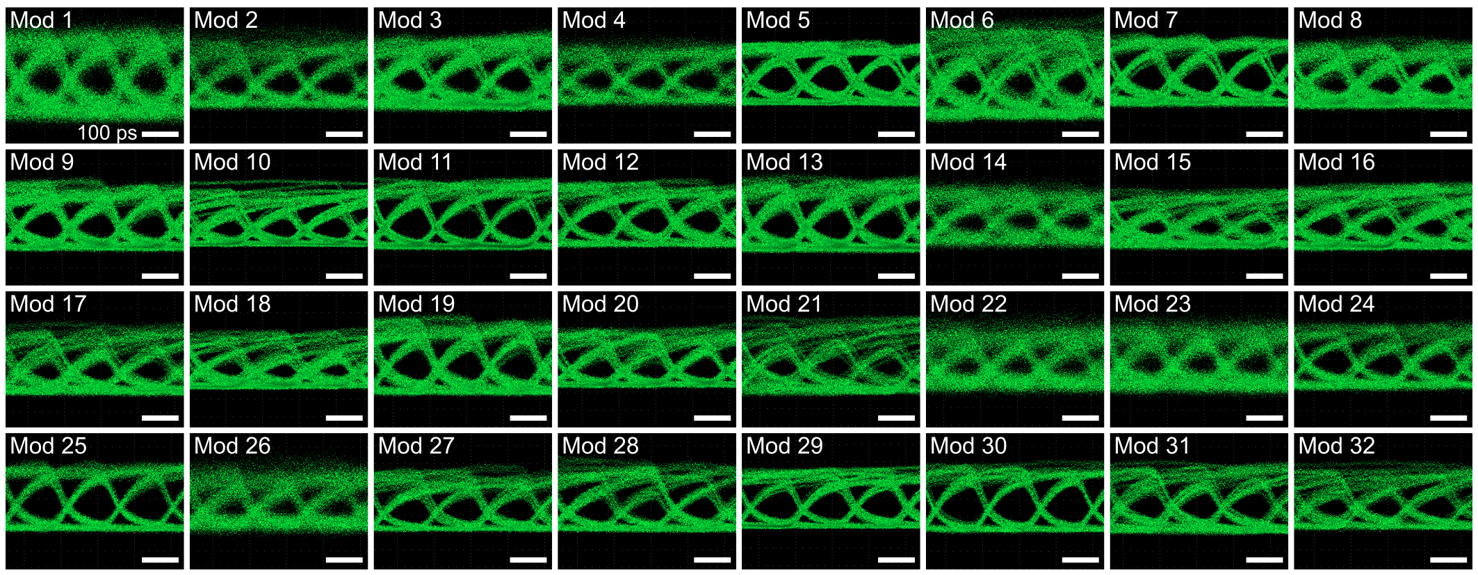
Eye diagrams of each modulator driven with 2 NRZ PRBS at 7 Gbits/s and Vpp = 6 V. We achieve 94% yield (30 out of 32 devices) with BER below the HD-FEC limit (BER ) at 7 Gbits/s, amounting to a total data rate of 210 Gbits/s for the chip. The eye diagrams display similar eye opening and OSNR as implied by the narrow spread of the histogram of Q-factor in Figure S6 of the Supplementary Information. The modulator number corresponds to that shown in the tiled optical micrograph in Figure 2b. The scale bars in all eye diagrams are 100 ps.
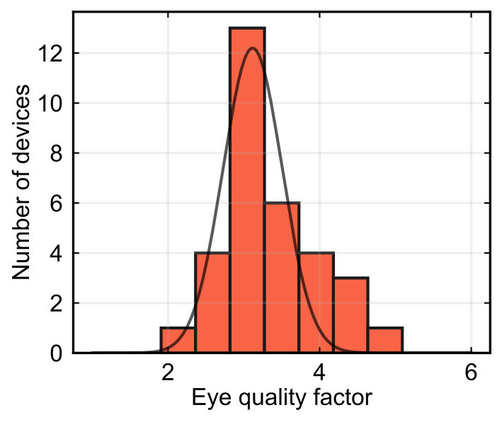
The eye diagrams display similar eye opening and OSNR as implied by the narrow spread of the histogram of Q-factor in Figure S6 of the Supplementary Information. The small variation of both modulation efficiency (V3dB) and bandwidth () enable modulators to transmit data with consistent performance across the chip at high speeds.
The modulators currently consume about 1.6 pJ/bit (from ), which is mostly dissipated by the termination resistor. The modulator impedance is dominated by the small device capacitance of around 180 fF. To reduce reflections caused by the impedance mismatch between the capacitive load and 50 transmission line, we terminated the modulator using a second set of probes with a d.c. block capacitor and 50 RF termination. This shunt termination reduces the voltage drop on the modulator by approximately 50%, so the applied voltage to the modulator is Vpp/2.
4 Design optimization towards Tbits/s data transmission
We show that with further optimization in device design, we can achieve stronger modulation extinction ratio and exceed the current aggregate data rate of 210 Gbits/s of the graphene transmitter chip. Figure 5a shows a schematic of an optimized device with higher dielectric constant () based on hafnia (\chHfO2) and, for comparison, Figure 5b shows a schematic of our current modulator.
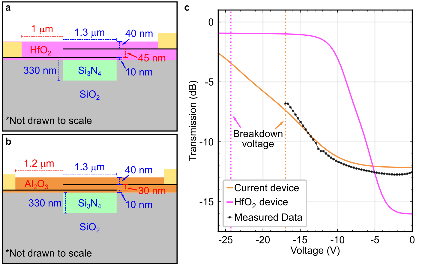
(a) Optimized device cross-section with high- gate. Here we simulate with \chHfO2. The blue and red labels indicate unchanged and changed parameters between the two designs, respectively. (b) Current device cross-section. The \chSi3N4 waveguide is 1,300 nm 330 nm and the graphene capacitor width is identical to the waveguide, 1.3 µm. The bottom encapsulating \chAl2O3 is 10 nm, the gate \chAl2O3 is 30 nm, and the top encapsulating \chAl2O3 is 30 nm. The electrodes are 1.2 µm away from the waveguides. (c) The expected transmission curve versus applied voltage for the optimized design in (a) as purple curve and current devices in (b) as orange curve which is in close agreement with the measured data (black dots). One can see that with the optimized design (purple curve) we expect to achieve a modulation depth of 15 dB before breakdown with 1 dB insertion loss as it reaches further into Pauli-blocking, in contrast to our current device (orange curve) where we achieve a modulation of 5 dB with 7 dB insertion loss.
The new design exhibits a stronger modulation extinction ratio due to both higher extrinsic doping and stronger overlap of the mode with the graphene. The extrinsic doping, , is about for Vpp = 6 V due to higher dielectric, corresponding to six times the mean intrinsic doping while for our current device in Figure 5b, is about for the same Vpp, corresponding to twice the intrinsic doping value. This stronger extrinsic doping in the optimized design leads to a greater contrast between graphene’s absorptive and transparent state. In addition, the mode overlap with the graphene in the device shown in Figure 5a is slightly higher, because \chHfO2 has higher refractive index than \chAl2O3 (2.07 versus 1.63 at 1,550 nm, respectively), further contributing to stronger extinction ratio. In order to ensure that the larger of \chHfO2 does not decrease the RC bandwidth, we design the device with an increased gate thickness from 30 nm to 45 nm and place the electrodes closer to the waveguide (1.0 µm compared to 1.2 µm for our current devices) to reduce graphene sheet resistance while adding negligible metal absorption. In Figure 5c we show the expected transmission curve versus applied voltage for the new design (purple curve) and, for comparison, we also show the transmission curve for our current device (orange curve) which is in close agreement with the measured data (black dots). One can see that with the new design we expect to achieve a modulation depth of 15 dB before breakdown with 1 dB insertion loss as it reaches further into Pauli-blocking, in contrast to our current device where we achieve a modulation of 5 dB with 7 dB insertion loss.
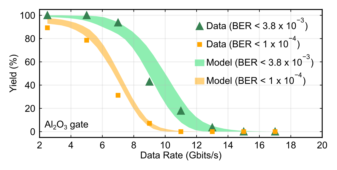
We show with optimized design we can achieve 80% yield at data rate up to 20 Gbits/s, indicating scalability of the platform to higher data rates. We show that optimizing device cross-section has stronger effect on yield than lowering graphene doping, confirming that doping effects can be mitigated solely by device design. Using Monte Carlo method (see the Supplementary Information for the description of our model), we simulate yield as a function of data rate for the different device design as shown in Figure 6.

Yield of devices in Figure 5a and Figure 5b as a function of data rate. The green triangle points correspond to the measured yield for BER , and the colored curves are simulated yield curves where the upper and lower boundaries are 95% interval (1.96 standard deviation). The green curve is the simulated yield for current device in (a) under variations of graphene doping measured in Figure S5, and is in good agreement with the measured data. The gray curve is the simulated yield for the current design with lower = and = . The red and blue curves are the simulated yields for the optimized high- gate devices with \chHfO2 for BERs and , respectively.
The upper and lower boundaries of the curves are 95% interval (1.96 standard deviation). We first confirm that the Monte Carlo model of our current device design with doping distribution from Figure S5 (green curve in Figure 6) is in good agreement with the measured yield (green triangles) for BER (also see Figure S7 in the Supplementary Information for BER ). The simulated yield for the optimized high- gate devices and similar distribution of graphene doping as current modulators for BER and (error-free for certain applications [18, 17]) are shown in the red and blue curves, respectively. In the gray curve of Figure 6, we show the simulated yield for a device with \chAl2O3 (same as current device) but with lower level of graphene doping and its variation, = and = , respectively, which are reported values for graphene encapsulated with BN [19, 20]. One can see that despite having larger distribution of graphene doping, the optimized devices with high- exhibit yield close to 100% at 12.5 Gbits/s at BER (red curve) in contrast to 12% yield at same data rate and BER of our current devices (gray curve). It is also evident that the optimized high- devices exhibit greater yield (close to 85%) even with stricter BER (blue curve) than current devices with assumed lower doping (gray curve), suggesting larger extrinsic doping improves data transmission more significantly than lowering and .
5 Conclusion
We have demonstrated that optimizing graphene-mode overlap and device capacitance of graphene-based modulators can minimize the effect of large inhomogeneities of CVD graphene films on device yield. We have achieved small variation in modulation efficiency and bandwidth for our modulators that allow them to transmit data with high fidelity. We also demonstrate the feasibility of data rates approaching Tbits/s with graphene modulators by further optimizing mode confinement and device capacitance using high- gate dielectric such as \chHfO2. This demonstration places graphene as the electro-optic material capable of simultaneously supporting high bandwidth, consuming low power, and achieving high integration density. In addition, as these modulators are not based on resonant cavities, they are capable of broadband and athermal operation [21], which paves the way for graphene-based wavelength and spatial division multiplexing to further enhance data transmission capacity.
Acknowledgment
The authors would like to thank Dr. Aseema Mohanty for the fruitful discussions and experimental support. This work was performed in part at the City University of New York Advanced Science Research Center NanoFabrication Facility and in part at the Columbia Nano Initiative (CNI) shared labs at Columbia University in the City of New York.
Funding
We gratefully acknowledge support Programmable Quantum Materials, an Energy Frontier Research Center funded by the U.S. Department of Energy (DOE), Office of Science, Basic Energy Sciences (BES), under award DE-SC0019443.
References
- [1] M Romagnoli, V Sorianello, M Midrio, et al. Graphene-based integrated photonics for next-generation datacom and telecom. Nature Reviews Materials, 3(10):392–414, 2018.
- [2] Z Li and N Yu. Modulation of mid-infrared light using graphene-metal plasmonic antennas. Applied Physics Letters, 102(13):131108, 2013.
- [3] CT Phare, YD Lee, J Cardenas, and M Lipson. Graphene electro-optic modulator with 30 ghz bandwidth. Nature Photonics, 9(8):511–514, 2015.
- [4] MA Giambra, V Sorianello, V Miseikis, S Marconi, A Montanaro, P Galli, S Pezzini, C Coletti, and M Romagnoli. High-speed double layer graphene electro-absorption modulator on soi waveguide. Optics Express, 27(15):20145–20155, 2019.
- [5] X Li, W Cai, J An, et al. Large-area synthesis of high-quality and uniform graphene films on copper foils. Science, 324(5932):1312–1314, 2009.
- [6] S Bae, H Kim, Y Lee, et al. Roll-to-roll production of 30-inch graphene films for transparent electrodes. Nature Nanotechnology, 5(8):574, 2010.
- [7] JD Buron, DH Petersen, P Bøggild, et al. Graphene conductance uniformity mapping. Nano Letters, 12(10):5074–5081, 2012.
- [8] Y Gong, X Zhang, G Liu, et al. Layer-controlled and wafer-scale synthesis of uniform and high-quality graphene films on a polycrystalline nickel catalyst. Advanced Functional Materials, 22(15):3153–3159, 2012.
- [9] LG Rizzi, M Bianchi, A Behnam, et al. Cascading wafer-scale integrated graphene complementary inverters under ambient conditions. Nano Letters, 12(8):3948–3953, 2012.
- [10] J Heo, K Byun, J Lee, et al. Graphene and thin-film semiconductor heterojunction transistors integrated on wafer scale for low-power electronics. Nano Letters, 13(12):5967–5971, 2013.
- [11] PC Theofanopoulos, S Ageno, Y Guo, S Kale, Q Wang, and GC Trichopoulos. High-yield fabrication method for high-frequency graphene devices using titanium sacrificial layers. Journal of Vacuum Science & Technology B, Nanotechnology and Microelectronics: Materials, Processing, Measurement, and Phenomena, 37(4):041801, 2019.
- [12] F Wang, Y Zhang, C Tian, et al. Gate-variable optical transitions in graphene. Science, 320(5873):206–209, 2008.
- [13] M Liu, X Yin, E Ulin-Avila, et al. A graphene-based broadband optical modulator. Nature, 474(7349):64–67, 2011.
- [14] Grolltex Inc. http://www.grolltex.com/.
- [15] K Verguts, J Coroa, C Huyghebaert, S De Gendt, and S Brems. Graphene delamination using ‘electrochemical methods’: an ion intercalation effect. Nanoscale, 10(12):5515–5521, 2018.
- [16] Y Zhu, Y Li, G Arefe, et al. Monolayer molybdenum disulfide transistors with single-atom-thick gates. Nano Letters, 18(6):3807–3813, 2018.
- [17] Govind P Agrawal. Fiber-optic communication systems, volume 222. John Wiley & Sons, 2012.
- [18] B Stern, X Zhu, CP Chen, et al. On-chip mode-division multiplexing switch. Optica, 2(6):530–535, 2015.
- [19] CR Dean, AF Young, I Meric, et al. Boron nitride substrates for high-quality graphene electronics. Nature Nanotechnology, 5(10):722–726, 2010.
- [20] J Xue, J Sanchez-Yamagishi, D Bulmash, and othersJ. Scanning tunnelling microscopy and spectroscopy of ultra-flat graphene on hexagonal boron nitride. Nature Materials, 10(4):282–285, 2011.
- [21] H Dalir, Y Xia, Y Wang, and X Zhang. Athermal broadband graphene optical modulator with 35 GHz speed. ACS Photonics, 3(9):1564–1568, 2016.
Supplementary Information
1 Graphene transfer via electrochemical delamination
We describe the electrochemical delamination transfer in Figure S8. We start with large area (75 mm 75 mm) CVD graphene on copper substrate (25 µm-thick) grown by Grolltex Inc. \citeSupsupgrolltex. We spin coat 400 nm-thick PMMA 495K A6 on graphene to provide mechanical support during the delamination. We dry the PMMA layer overnight at ambient conditions without additional baking steps. For the electrolyte we prepare 1M \chNaOH solution. The PMMA/graphene/Cu foil acts as a cathode and another bare Cu foil as an anode. We apply –2.2 V to the graphene sheet with respect to the copper anode, and slowly submerge both the anode and PMMA/graphene/Cu cathode into the electrolyte. The PMMA/graphene stack begins to delaminate due to ion intercalation effect \citeSupsupverguts2018graphene and floats due to surface tension. The delamination takes about 10 - 15 seconds for film size around 20 mm x 20 mm. We then transfer the floating PMMA/graphene stack to a fresh de-ionized (DI) water bath using a glass slide to rinse the electrolyte. We rinse the PMMA/graphene stack in two DI water baths, 5 minutes in each bath. We transfer the graphene film onto a substrate with flat surface pre-treated with \chO2 plasma. Cleaning the substrate with \chO2 plasma strips residues and makes the surface hydrophilic, which facilitates the removal of trapped water between graphene and the surface during the drying step. We dry the wet substrate in a vacuum desiccator with a base pressure of around 0.5 Torr for at least 24 hours to pump out residual water. Fully drying the sample significantly reduced tears in the graphene. After vacuum-drying the sample, we bake it on a hot plate at 180 for two hours and strip the PMMA film in acetone bath for at least 1 hour.
2 Modeling device yield with Monte Carlo Simulations
2.1 Screening influential parameters with sensitivity analysis
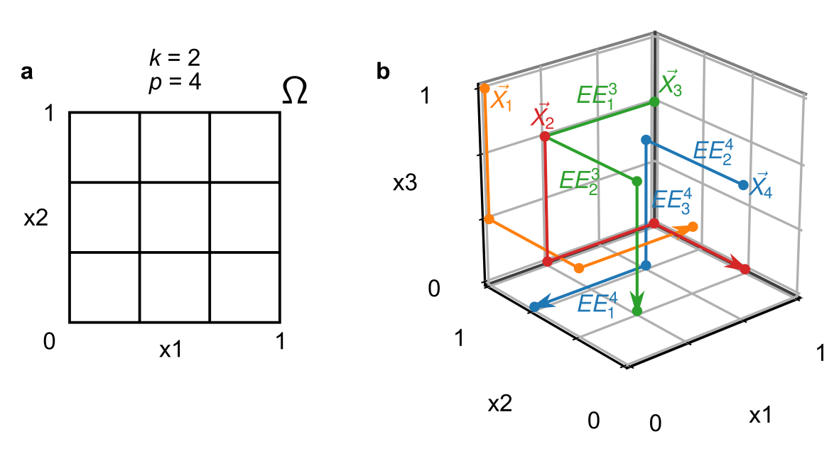
We first perform sensitivity analysis with elementary effect test (EET) method \citeSupmorris1991factorial to identify device parameters that have strong influence on extinction ratio. By identifying the most influential parameters, we focus on varying these variables while fixing others constant in our Monte Carlo simulations to save computational cost \citeSupwaqas2017sensitivity.
EET method is based on calculating a number of differential ratios, called elementary effects (EEs), for a given input vector, from which statistics are computed to derive sensitivity information. To illustrate EET, let us assume there are input variables, such as waveguide width, thickness, etc., and is the input vector. Next, we assume that each parameter is varied across -levels, such that the whole -dimensional input space is discretized as a -point grid, which we call it region . We show with and in Figure S1a, and with and in Figure S1b as examples. Let be the output of interest (e.g. extinction ratio, insertion loss, etc.) from a model ,
| (S1) |
The gist of EET is to randomly sample number of input vectors or initial points (, , …, ) and then move these points in by randomly changing each variable in one-at-a-time fashion, creating a ()-point trajectory for each initial point. We illustrate this with input points (, …, ) sampled in with and grid in Figure S1b. Each input point randomly moves in a basis direction (, , or in Figure S1b), and during each step through the trajectory we calculate an EE defined by:
| (S2) |
where , is the variable being moved (), and is incremental step chosen from the set (in Figure S1b, for example, we choose ). Some EEs are labeled in Figure S1b to their corresponding edges. For a given , sufficient number of samples, , should be chosen such that the trajectories effectively cover without trading off computational cost.
Once all the EEs are computed for all trajectories taken by randomly sampled input vectors, for each input factor we measure and , which are mean and standard deviation of EEs related to input , defined as \citeSupcampolongo2007effective:
| (S3) | |||
| (S4) |
These statistical parameters of EEs provide a direct qualitative knowledge on the influence of input on the model. The mean, assesses the overall influence of a parameter on the model output, and describes non-linear effects \citeSupmorris1991factorial. A large indicates that the parameter is interacting with others in a non-linear way because its EEs vary greatly depending on which trajectories they originate from.
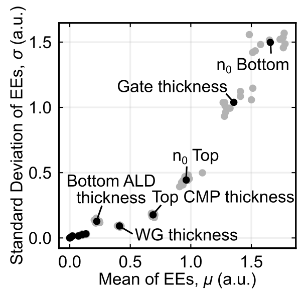
We perform EET for our modulator design, which has a total of 12 parameters, and determine that graphene residual doping (for both top and bottom sheets) and gate thickness are the most influential parameters on extinction ratio as they have the greatest . As expected, parameters that directly relate to Pauli-blocking in graphene and control the degree of graphene-mode overlap are the most influential parameters. Moreover, since bottom graphene sheet has stronger interaction with the mode, its level of doping is expected to have stronger influence on extinction ratio than the top graphene doping. For subsequent Monte Carlo iterations, we fix other parameters constant at their designed values to save computational cost. We run [45] independent studies and plot the mean and standard deviations of EE for each parameter in Figure S2. The black dots are average values of and from [45] iterations. In the background we superimpose all the points from [45] iterations as gray dots to show the full statistics.
2.2 Implementation of Monte Carlo simulations
We perform Monte Carlo simulations based on statistical measurements of the most influential parameters on extinction ratio identified using EET sensitivity analysis. These are graphene residual doping and gate dielectric thickness, and measurements of these parameters are summarized in Table S1. We measure graphene residual doping, , by measuring charge neutral points, , of 28 graphene field-effect transistors (GFETs) evenly placed over similar chip area to our transmitter chip (8 mm 1 mm), and calculate via the relation , where the capacitance is measured via graphene Hall bar structures. We plot residual doping histogram in Figure S5, whose measured mean and standard deviation from normal distribution fit are = and = , respectively. For the gate dielectric thickness we measure a standard deviation of 2 nm. We measure the thickness variation by depositing 30 nm (target thickness) ALD \chAl2O3 on silicon substrate and measure the thickness of film at various points (across 8 mm 1 mm area) with an ellipsometer. Dielectric constant is deduced from capacitance measurements using a graphene Hall bar as = 4.2.
| Parameter | Mean | Std |
|---|---|---|
| n0 ( cm-2) | 7.3 | 2.3 |
| Gate thickness (nm) | 29.1 | 2.0 |
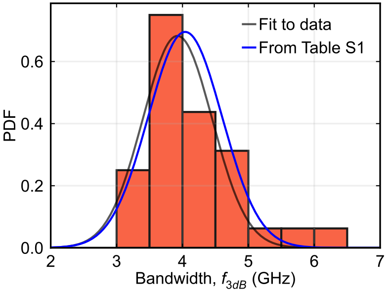
We also measure contact resistance and Hall mobility (for sheet resistance) of = 10.5 1.3 kµm and = 1420 26 cm/Vs, respectively. We finally note that our measured variations of RC related parameters (Table S1, , , etc.) provide similar distribution of calculated bandwidth as our measured data in Figure 3c, as shown in Figure S3. The bandwidth calculated from variations of RC related parameters (blue solid curve) has similar mean and standard deviation (mean = 4.0 GHz, std = 0.56 GHz) as the data and its fit (black solid curve).
We describe the flow of our Monte Carlo simulations for emulating device performance and data transmission yield in Figure S4. We first construct the input voltage square pulses in the time domain at a given data rate, , and find its Fourier coefficients (Figure S4a). We subsequently calculate device bandwidth by sampling RC related parameters from our measured distributions and compute as a function of frequency (Figure S4b). We multiply with Fourier coefficients of the input signal to deduce the voltage applied to the modulator,, limited by its bandwidth (Figure S4c). We construct the modulator cross-section using sampled doping concentration for bottom and top graphene and gate thickness as shown in Figure S4d. Then, we extract the extinction ratio due to with a finite difference eigenmode (FDE) solver (Lumerical \citeSuplumerical) and calculate the BER.
We compute BER by first calculating Q-factor \citeSupsupagrawal2012fiber:
| (S5) |
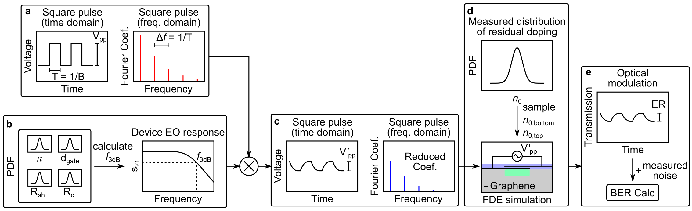
(a) We construct the input voltage square pulses (to emulate NRZ PRBS) with peak-to-peak amplitude equal to the drive voltage reduced by 50 termination (Vpp/2) in the time domain at a given data rate, , and find its Fourier coefficients. (b) We calculate the device RC bandwidth by sampling RC related parameters – dielectric constant (), gate thickness (), sheet resistance (), contact resistance () – and calculate and resulting as a function of frequency. (c) We multiply the Fourier coefficients of the square pulse with the frequency response of the device to calculate the new pulse applied to the device. This new amplitude () is applied to the modulator. (d) We sample graphene residual doping for both sheets of graphene in the capacitor and gate thickness from (a) to create a new device geometry, and calculate the extinction ratio with the drive voltage (). with a FDE solver. (e) We use the calculated extinction ratio from (d) in order to calculate the quality factor and BER according to Equation S5.
where and are optical power and RMS noise of level 1 and level 0, respectively, measured by the receiver, and is the extinction ratio, , and is the total RMS noise normalized to level 0. We measure average of [0.11], which we use in the Monte Carlo simulations. Once we calculate the Q-factor, the BER is equal to BER = 0.5erfc(Q/) [17], where erfc is the complementary error function.
3 Supplementary Figures
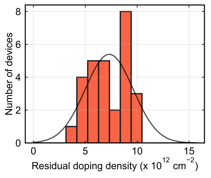
We characterize residual doping in graphene sheets prepared with electrochemical delamination (see Figure S8). We measure the Dirac point of graphene channels in GFETs fabricated evenly throughout a test chip of similar size to our graphene transmitter chip (8 mm 1 mm). We sweep the gate voltage and measure the voltage that yields minimum drain-source current. We calculate the residual doping from this voltage, by , where C is the measured GFET capacitance of and is the positive elementary charge. The solid line is the normal distribution fit to the data with mean = and standard deviation = (32% of mean).
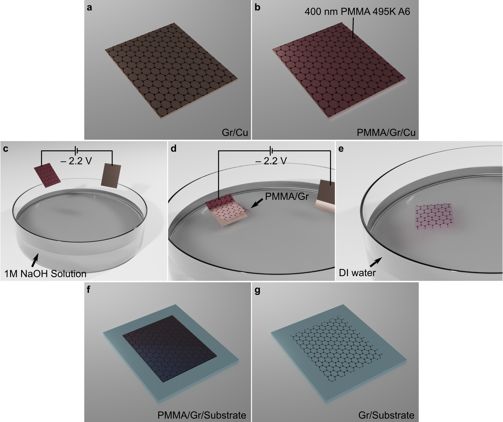
(a) We start with large area (75 mm 75 mm) CVD graphene on copper substrate (25 µm-thick) grown by Grolltex Inc. \citeSupsupgrolltex. (b) We spin coat 400 nm-thick PMMA 495K A6 on graphene to provide mechanical support during the delamination. We dry the PMMA layer overnight at ambient conditions without additional baking steps. (c) For the electrolyte we prepare 1M \chNaOH solution. The PMMA/graphene/Cu foil acts as a cathode and another bare Cu foil as an anode. (d) We apply –2.2 V to the graphene sheet with respect to the copper anode, and slowly submerge both the anode and PMMA/graphene/Cu cathode into the electrolyte. The PMMA/graphene stack begins to delaminate due to ion intercalation effect \citeSupsupverguts2018graphene and floats due to surface tension. The delamination takes about 10 - 15 seconds for film size around 20 mm x 20 mm. (e) We transfer the floating PMMA/graphene stack to a fresh de-ionized (DI) water bath using a glass slide to rinse the electrolyte. We rinse the PMMA/graphene stack in two DI water baths, 5 minutes in each bath. (f) We transfer the graphene film onto a substrate with flat surface pre-treated with \chO2 plasma. We dry the wet substrate in a vacuum desiccator with a base pressure of around 0.5 Torr for at least 24 hours to pump out residual water. (g) We bake the sample on a hot plate at 180 for two hours and strip the PMMA film in acetone bath for at least 1 hour.
unsrt \bibliographySupSReferences