First-Principles Prediction of Electronic Transport in Experimental Semiconductor Heterostructures via Physics-Based Machine Learning
Abstract
First-principles techniques for electronic transport property prediction have seen rapid progress in recent years. However, it remains a challenge to model heterostructures incorporating variability due to fabrication processes. Machine-learning (ML)-based materials informatics approaches (MI) are increasingly used to accelerate design and discovery of new materials with targeted properties, and extend the applicability of first-principles techniques to larger systems. However, few studies exploited MI to learn electronic structure properties and use the knowledge to predict the respective transport coefficients. In this work, we propose an electronic-transport-informatics (ETI) framework that trains on ab initio models of small systems and predicts thermopower of silicon/germanium heterostructures beyond the length-scale accessible with first-principles techniques, matching measured data. We demonstrate application of MI to extract important physics that determines electronic transport in semiconductor heterostructures, breaking from combinatorial strategies pursued especially for thermoelectric materials. We anticipate that ETI would have broad applicability to diverse materials classes.
Semiconductor heterostructures have brought about tremendous changes in our everyday lives in the form of telecommunication systems utilizing double-heterostructure lasers, heterostructure light-emitting diodes, or high-electron-mobility transistors used in high-frequency devices, including satellite television systems [1]. Silicon (Si)/germanium (Ge) heterostructures, in particular, have emerged as key materials in numerous electronic [2, 3, 4, 5], optoelectronic [6, 7, 8], and thermoelectric devices [9, 10], and promising host of spin qubits [11]. Recent developments of nanofabrication and characterization techniques achieved great control over the growth of Si/Ge heterostructures [12, 13, 14, 15, 16]. Nevertheless, fabrication of heterostructures is strongly affected by strain relaxation in component layers [5], and the resulting electronic properties show high variability due to inconsistent fabrication dependent structural parameters [17, 10, 18, 10]. A few theoretical studies discussed the effect of non-idealities on electronic properties of heterostructures [19, 20], however, these studies were parametric in nature. It is essential to acquire a comprehensive understanding of the complex relationship between growth dependent parameters and electronic properties, to attain targeted semiconductor heterostructure design with reliable electronic performance. Ab initio techniques enable prediction of materials properties with minimal experimental input, however, often come with large computational costs. In particular, the calculations of electronic transport coefficients (such as, thermopower or conductivity) require large number of individual energy calculations and computational costs can accrue quickly. It remains a challenge to model electronic transport coefficients of technologically relevant heterostructures incorporating full structural complexity, representing the vast fabrication dependent structural parameter space.
Recent studies demonstrated the ability of data driven techniques to predict the results of new calculations at little additional computational cost, using previous ab initio model data as input [21, 22]. The use of machine learning (ML) models showed remarkable successes in accelerating atomistic computations and extending applicability of first-principles techniques to predict properties of larger systems [23, 24, 25, 26]. Machine-learning-based materials informatics (MI) are increasingly being used to accelerate design and discovery of new materials and structures [27, 28, 29], facilitated by large amounts of data generated with high-throughput density functional theory (DFT) calculations [22] or available through databases [30, 31]. Most of these studies aimed at identifying structures that optimize the target property. ML models are being used to explore the relationship between structure and electronic transport property, especially in the context of thermoelectric materials. However, the focus remained on combinatorial approaches to identify compounds that optimize the relevant electronic transport coefficients, such as thermopower [32] or electronic power factor [33]. Only recently, some attempts have been made to use MI to learn and predict atomic scale dynamics [34]. Few studies exploited ML techniques to establish relationship between the electronic structure properties and the respective transport coefficients [35, 36]. A vast amount of information is generated during a single ab initio electronic structure property calculation. Therefore, there is great benefit to develop approaches that can harvest information from previous calculations to predict properties of new systems, a priori.
In this work, we propose a first-principles-based electronic-transport-informatics (ETI) framework that is trained on the electronic structure properties of small systems and predicts transport coefficients, namely the thermopowers of experimental semiconductor heterostructures. The framework is built on the hypothesis that functional relationships between local atomic configurations, , and their contributions to global energy states, , are preserved when the configurations are part of a nanostructure with different composition and/or dimensions. The rationale for the hypothesis is rooted in the fundamental insight that material’s physical properties, ranging from mechanical to electronic, are intimately tied to the underlying symmetry of the crystal structure [37]. This conjecture allows one to probe the local configuration-energy state relationships, , in few-atom fragment units with varied atomic environments, and harness the information to predict ’s that develop in larger nanostructures, hosting similar local environments, . We implement this hypothesis to extrapolate the insight acquired from small ab-initio models to predict local ’s in experimental semiconductor heterostructures. We estimate the global energy states of the heterostructure with known ’s by assimilating the predicted ’s. The energy states are then used to predict Seebeck coefficients () or thermopowers, that are validated against numerical results obtained with first-principles methods (DFT), or experimental data. We anticipate that the hypothesis can be similarly applied to obtain other electronic transport coefficients. Our ETI framework thus establishes that MI can be exploited to address the gap between ideal ab-initio models and systems realized with nanofabrication techniques.
I Results and Discussion
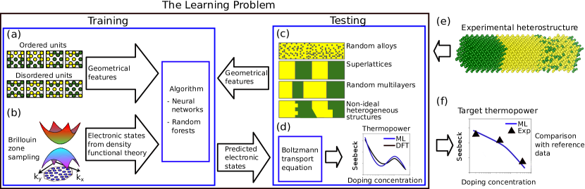
Figure 1 shows the outline of the ETI framework that provides first-principles prediction of thermopowers of experimental Si/Ge heterostructures. The ML model learns the relationships between atomic configurations () and electronic bands (, panel (b)) present in 16-atom fragment training models (cartoons in panel (a)), and predicts environment-electronic state correlations, , existing in larger heterostructures (panels (c, e)). The components of our ETI framework are: (1) creation of a data resource to harvest , (2) formulation of a representation that can uniquely describe , and help characterize , in a fragment unit or target heterostructure, (3) choice of ML algorithms to discover correlations in training data, and, (4) testing ML predictions for new structures against known data.
(1) Creation of Data Resource: We explored materials property databases, such as Material Project [30] and NOMAD Repository & Archive [31] to collect training data. However, the electronic structure property data of only limited number of Si/Ge structures are available. Additionally, the available data do not provide necessary sampling of the structure Brillouin zones (BZ) to converge electronic transport coefficients, requiring us to create our own data resource. In order to minimize data generation efforts, we limit the number of electronic property calculations, and instead, mine the large amount of information generated in individual calculations. In our recent publications, we presented extensive investigations of the electronic structure and transport properties of Si/Ge heterostructures [38, 39, 40, 41]. These past data and insights greatly facilitate the development of the ETI framework. Based on the acquired insights [39, 40, 41], we follow two strategies: (i) careful choice of fragment training units, and (ii) utilizing atomistic information generated from individual DFT calculations of the units as training data.
The first strategy is implemented by choosing Si/Ge systems with varied strain environment as training fragments. The choice is guided by the fact that the bands of Si/Ge heterostructures are significantly affected by strain [39, 41, 40, 42]. Application of strain led to more than an order of magnitude variation in electronic properties over the non-strained materials [43, 44, 45]. In heterostructures, strain is generated due to various mechanisms including structural (lattice mismatch, presence of defects), thermal expansion or chemical (phase transition) changes. Naturally, the strain environment is variable, and the resulting electronic properties are unpredictable, making the problem ideal for the application of ML techniques. Panel (a) of Fig. 1 shows cartoon representations of the two categories of the fragment training systems. The 16-atom models include ordered layered Si/Ge superlattices (SLs) and disordered Si-Ge “alloys” (see Methods section for details). We acknowledge that the small size of the model units along with the imposed periodic boundary conditions do not reflect true randomized alloy configurations. Nevertheless, the models allow us to explore in these binary systems as a function of variable atomic environments. The remarkable successes shown by MI approaches using DFT generated data [21, 22] inspired us to use DFT to generate training data. The DFT computed electronic structure properties and energy bands of the model units serve as training data and benchmark for cross-validation tests.
(2) Formulation of Representation: Identification of a minimal set of features is crucial to formulate relevant structure-property relationships [21, 46, 47]. For our ETI framework, it is essential that the features describe sub-Angstrom-scale structural details because of the following reasons: (i) electronic transport in a heterostructure is highly sensitive to local structural environment, and (ii) success of ETI is based on the hypothesis that is preserved across structures hosting similar environment, and determines the electronic transport properties. Thus, it is essential that the correlations, , are built upon fine details of , to ensure the transferability of the framework across structures. However, is expected to be multivariate and highly nonlinear. Hence, we are tasked to identify a feature subset that is strongly correlated with the electronic transport properties, from a large structural parameter space. A diverse set of elemental properties are used as features in MI [46]. Since our heterostructures are binary, the elemental-property-based features differ only slightly across the various configurations and are not expected to provide unique information to develop . We consider only one elemental-property-based feature, computed from the electronegativity difference of the species (Si, Ge). Instead, we include multiple global and local structural features that are directly affected by strain. Global features include atomic composition of the systems (e.g., Ge concentration) and lattice constants ().
To determine the relevant local features describing , we express the structures as crystal graphs that encode both atomic information and bonding environments [48, 49, 26]. Crystal graph based ML models have shown great success in recent years for first-principles materials property prediction [46, 48, 49, 26]. Figure 2(a) shows a representative crystal graph of a typical SiGe configuration. The atom and the neighboring atoms form nodes, and the interatomic distances constitute the edges. We identify the neighboring atoms from Voronoi tessellations (VT) of the crystal structure. Figure 2(b) shows VT of a model Si4Ge4 SL. The neighbors occupy adjoined cells and share faces in the tessellations. Thus, each face of a Voronoi cell marks a specific nearest neighbor of the selected atom. Figure 2(c) shows a representative Voronoi cell in a representative Si/Ge configuration. The VT approach is particularly beneficial for our study since the tessellations are uniquely defined for a given local environment, and are insensitive to global dimensions of the structure. Therefore, VT-derived features help transfer ’s across structures of varying dimensions. VT-derived features has facilitated successful MI prediction of formation enthalpies [46].
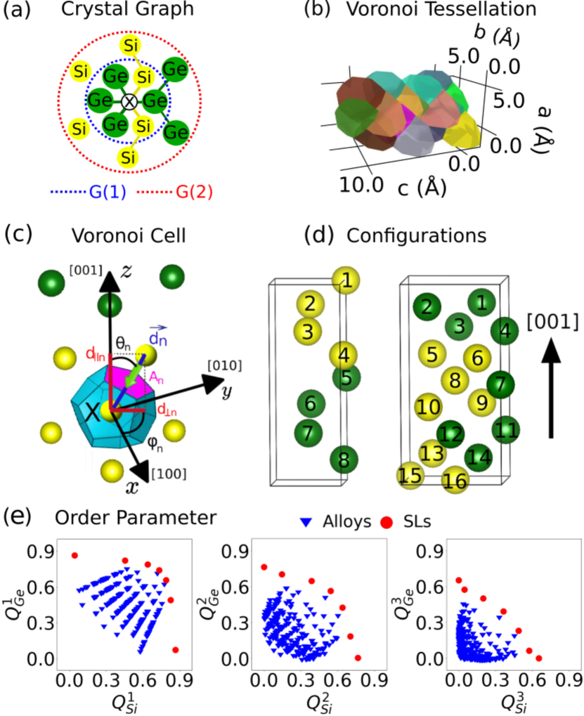
In total, we describe of each configuration with 100 features. We have included extensive discussions of all the features in SI. The relative feature importance data shown in Fig. S7 reflects the strong influence of VT-derived features on the performance of the ETI framework.
In our feature set, the local spatial ordering of atoms is represented by order parameters, [50, 46], where
| (1) |
The paths connect all neighboring atoms up to a specified order in the crystal graph, e.g., (blue), (red) in Fig. 2(a). We limit to order (), because higher order graphs do not significantly impact the predictions, however, the cost to construct them increases proportionally with the volume containing the neighbors, order3. The Kronecker delta function in the numerator further restricts consideration of paths connecting only atoms of same type as , yielding species aware crystal graphs. For example, the paths connecting the Si (yellow) or the Ge (green) circles in Fig. 2(a) assume atom to be of type Si (yellow) or Ge (green), respectively. A typical step along a path connecting neighbors to is shown by the arrow (green) in Fig. 2(c). The step crosses the face of index and area (magenta), normal to its direction. The ratio between area, , and the sum over all areas the step could possibly cross, , that are part of other non-backtracking paths, determines the fractional weight (Eq. 1). Thus, the fractional weight of each step can be understood as the probability of taking the step. The product of fractional weights of all steps in a path determines the effective weight, the probability of choosing the path. The sum of the effective weights of all possible non-backtracking paths in results in . Figure 2(e) shows the variations of and , for the 357 ordered (7) and disordered (350) fragment units. The scatter plot illustrates that we can distinguish each SiGe configuration by and . For example, the distinct clusters of data points representing the layered SL and the “alloy” configurations can be noted. Thus, the order parameters are highly effective in distinguishing configurations with different degrees of structural ordering. From left to right in Fig. 2(e), higher order parameter values decrease at a fast rate for disordered “alloy” configurations, but only slightly for SLs.
To further distinguish the anisotropic bonding environment of a SL compared to a disordered unit, we define directionally-biased order parameters, . The bias is implemented by calculating the fractional weights using projections of along a chosen direction only (see SI). In Table 1, we show ’s of the atoms of the Si4Ge4 SL configuration shown in Fig. 2(d). As a reference, these order parameters are all equal to for bulk systems. The in-plane order parameters, , , are equal, due to the rotational symmetry of the configuration around -axis, aligned along [001]. In comparison, is lower and decreases faster with the order number, reflecting heterogeneous stacking along direction. can be used to identify the different atomic environments along direction, e.g., represents interface atoms and indicates inner atoms. The order parameter values are higher for inner atoms and lower for interface atoms. This is due to the presence of greater number of same species neighbors resulting in more paths contributing to order parameters of inner atoms. The order parameters also highlight the reflection symmetry with respect to the plane, yielding identical values for atom pairs such as and . In comparison, the order parameters of the Si8Ge8 random “alloy” configuration shown in Fig. 2(d) do not show any specific pattern and decrease fast with the order number reflecting the disordered atomic arrangement (See SI Table III). In Fig. S6, we show the species-aware, directionally-biased order parameters of all SL and “alloy” training units.
| Atom | # | |||||||||
|---|---|---|---|---|---|---|---|---|---|---|
| Si | 1 | 0.55 | 0.55 | 0.51 | 0.49 | 0.49 | 0.45 | 0.36 | 0.36 | 0.29 |
| Si | 2 | 0.95 | 0.95 | 0.89 | 0.64 | 0.64 | 0.53 | 0.43 | 0.43 | 0.34 |
| Si | 3 | 0.95 | 0.95 | 0.89 | 0.64 | 0.64 | 0.53 | 0.43 | 0.43 | 0.34 |
| Si | 4 | 0.55 | 0.55 | 0.51 | 0.49 | 0.49 | 0.45 | 0.36 | 0.36 | 0.29 |
| Ge | 5 | 0.53 | 0.53 | 0.49 | 0.47 | 0.47 | 0.46 | 0.37 | 0.37 | 0.30 |
| Ge | 6 | 0.97 | 0.97 | 0.94 | 0.70 | 0.70 | 0.58 | 0.47 | 0.47 | 0.36 |
| Ge | 7 | 0.97 | 0.97 | 0.94 | 0.70 | 0.70 | 0.58 | 0.47 | 0.47 | 0.36 |
| Ge | 8 | 0.53 | 0.53 | 0.49 | 0.47 | 0.47 | 0.46 | 0.37 | 0.37 | 0.30 |
The order parameter feature is particularly important since directional ordering controls the atomic orbital contributions to energy bands in Si/Ge heterostructures [41]. We have included further illustrations of the order parameter concept in SI.
(3) Choice of ML algorithm: We use supervised neural network (NN) and random forests (RF) algorithms to learn , and compare performance of the two algorithms in predicting for given .
NN Model: Our model consists of an input layer consisting of 128 nodes, three fully connected hidden layers each with 256 nodes, and an output layer with nodes equal to the number of energy values, : . We consider six valence and six conduction bands , and a -point mesh to sample the respective BZ, resulting in values for each training configuration. We tested that such sampling of -values yields necessary convergence of Seebeck coefficients [39, 41] (Fig. S9). The size of the model input is equal to the number of features considered. We use 100 features to describe each training unit and a batch size of 32 structures to train the model. Therefore, the NN algorithm is supplied with input values at each iteration during training. The NN model is tasked to formulate , relating features of and the target electronic states , parametrized by weights . The training is performed by iteratively updating the weights to minimize the mean absolute error (MAE) between the calculated and the predicted energies,
| (2) |
We employ the ADAM stochastic optimization method for gradient descent to minimize the loss function (MAE). The high-level NNs are implemented using the Keras library [51] written in Python. In all NN models, the Rectified Linear Unit activation functions are utilized. Five-fold cross-validation tests are performed to avoid overfitting. The optimized weights,
| (3) |
are then used to predict values for unknown systems.
RF model: RF models [52] are shown to be computationally inexpensive and robust to overfitting of data [46]. The algorithm assembles results of several decision trees, each built from random selection of training data that include both features and example training energy values. The selected data is further partitioned into subsets based of decision rules that constitute branches of the tree. For example, the subsets can be formed based on order parameter values, e.g., , representing different atomic environments (see Table 1). The decision rules identify features that minimize the intrasubset variation of electronic energies. The leaves of the tree are then assigned to an energy value that maximizes fitting over the subset data. Such tree generation process is then repeated for other random subsets of training data. The final predictions are obtained by averaging the predicted energies over all trees. We implement the RF module available in the scikit-learn Python package [53]. The input and output are identical to the ones used for the NN algorithm. We use 100 regression trees per ensemble and set all other parameters to default values recommended for the package. We did not observe any notable change in the predicted energy values by increasing the number of trees to 200 and 300.
In the following, we discuss the performance of the two ML algorithms in predicting electronic transport coefficients of three classes of SiGe heterostructures: (1) ideal strained superlattices, (2) non-ideal heterostructures with irregular layer thicknesses and imperfect layers, and (3) experimental heterostructures.
I.1 Strained Ideal Superlattices
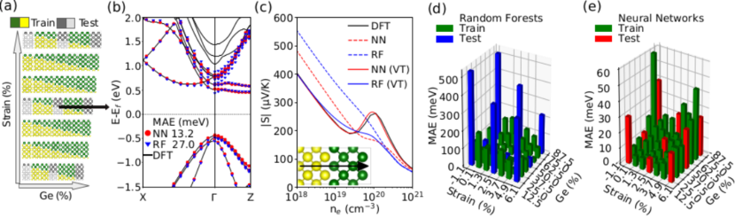
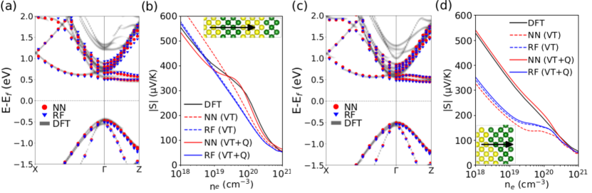
We test the effectiveness of our ETI framework in predicting the thermopowers of ideal SLs, considered to be grown on substrates inducing epitaxial strain. We use the term ideal to refer to SLs with sharp interfaces. We consider 7 applied strain values ranging uniformly from to , resulting in 49 different SLs, depicted by cartoons in Fig. 3(a). Strains in the range of have been observed in Si/Ge nanowire heterostructures with compositionally abrupt interfaces, grown via the VLS process [54]. We consider some extreme strains to probe the predictive power of our ML models. The models are trained on 40 and tested on 9 SLs. In Fig. 3(b), we show the bands of a strain-symmetrized Si4Ge4 SL along symmetry directions of a tetragonal BZ. Both NN and RF algorithms predict energies remarkably close to DFT results, with MAEs given by 13.2 meV and 27.0 meV, respectively. The train and test MAE for the two predictions are shown in Fig. 3(d,e). MAE is relatively small for small strain systems and higher for high strain boundary values. Both the algorithms yield small train MAE while their testing errors are considerably different. For example, the NN-predicted degenerate bands at 0.8 eV along compare well with DFT results but the RF predictions deviate moderately. The band gap is also predicted better by the NN algorithm. In Fig. 3(c), we show of strain-symmetrized -type Si4Ge4 SLs as a function of carrier concentration, , which can be controlled by chemical or electrostatic doping methods [55]. Within BTE, is obtained by integrating a function including band energies, Fermi-Dirac distribution function and transport distribution function [56] over the respective BZ, as outlined in the Method section. Thus, the discrepancy in predicted bands leads to an accumulated error in prediction. The closer match of the NN-predicted lowest conduction bands with the DFT results in a better prediction of the resulting . Figure 3(c) shows that the predictions significantly improve when the ML models are trained using VT-derived features (solid curves) in addition to using only global features (dashed curves). This analysis emphasizes the importance of considering local environment features in order to predict thermopowers with higher accuracy.
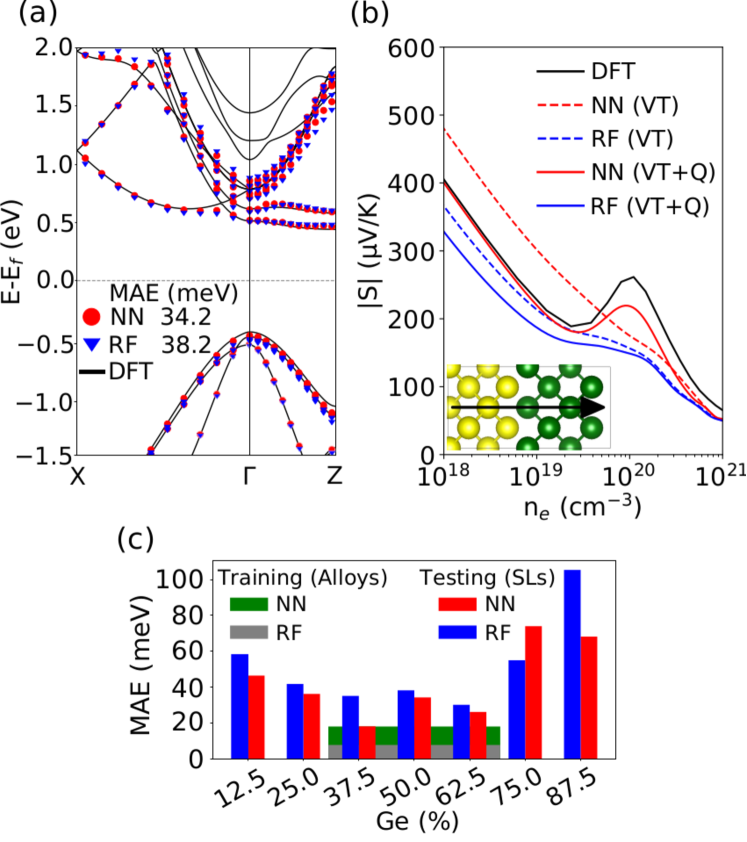
In the following, we provide further discussion on the effectiveness of training ML models with features describing local atomic environments. In Fig. 4(a,b), we show the bands of a strain-symmetrized Si4Ge4 SL along with the corresponding . Similar to Fig. 3(b), the predictions match DFT results closely, with MAEs of 34.2 meV (NN) and 38.2 meV (RF), respectively. The remarkable aspect of these results is that the ML models are trained only on disordered fragment units and the predictions are made for ordered structures. These results provide a direct demonstration of our central hypothesis that the local atomic configurations-energy states relationship, , is preserved across configurations with different compositions. Figure 4(b) further highlights that training ML models including order parameter features improves predictions (solid curves). The MAE for the 7 relaxed SL configurations of varying Ge concentrations are shown in Fig. 4(c). The high MAE for the samples with the lowest and the highest Ge concentrations can be attributed to the limited number of disordered training units with similar Ge concentrations (see Fig 2(e)). The order parameter maps thus provide great insight into the expected performance of the ML models for different test structures. These results demonstrate that our ML models capture the necessary information regarding the true interatomic interactions present in these binary heterostructures in an unbiased manner. We leverage this knowledge and the central hypothesis to probe in 16-atom ordered and disordered fragment units, and extrapolate the insight to predict the energy states and transport coefficients of larger heterostructures as demonstrated below. We train the ML models with both global and VT-derived features to achieve this objective.
I.2 Non-Ideal Heterostructures
To prove the transferability of the ETI framework, we task our ML models to predict electronic transport properties of 32-atom non-ideal SLs. The two types of “non-idealities” we probe are represented by SLs with irregular layer thicknesses (Fig. 5(b)), and imperfect layers (Fig. 5(d)). These systems are explorable with first-principles techniques, but larger in size compared to the 16-atom training units. As a result, we face a challenge to validate the ML predicted bands against DFT results due to the size difference between train and test structures. The ML models predict energy bands sampling the first BZ of 16-atom models, as shown in Fig. 3 and 4. However, the 32-atom test systems have a smaller BZ and as a result, several bands are zone-folded. Additionally, as the system size increases, so does the number of bands in both valence and conduction zones, making it challenging to keep track of. We resort to a band structure unfolding technique that allows to identify effective band structures (EBS), by projecting onto a chosen reference BZ [57, 58]. We obtain the EBS of different 32-atom test configurations by projecting the DFT computed bands onto the BZ of 16-atom reference cells, and compare with the ML predicted bands sampling a similar size BZ. This technique has been illustrated for different random substitutional alloy compositions: to probe to which extent band characteristics are preserved at different band indices, and -points, compared to the respective bulk systems (see Methods section for details). Although this technique has not been applied to probe SL bands, we argue that these systems, especially non-ideal SLs, are closer to alloy systems due to broken translational symmetry. In Fig. 5(a), we show the EBS of a 32-atom random multilayered heterostructure, Si4Ge4Si5Ge3. Here the indices represent the number of MLs in each component layers, as can be identified from the configuration in the inset of Fig. 5(b). Figure 5(c) shows the EBS of a 32-atom imperfect layer heterostructure, as represented by the configuration in the inset of Fig. 5(d). The remarkable agreement between ML-predicted bands and EBS can be noted from both the figures. Similar to the example shown in Fig. 3, the NN algorithm provides a slightly better estimate of band gap. As demonstrated in Fig. 5(b,d), the inclusion of the order parameters () is crucial for accurate prediction of thermopower. We tested the ML models on a class of such non-ideal heterostructures and include other results in SI (see Fig. S11).
I.3 Experimental Heterostructures
As we discussed previously, the domain of application of first-principles approaches is often limited to ideal systems that do not reflect the structural complexity of experimental heterostructure, mainly due to the required computational expenses. As a consequence, we resort to parametric approaches to predict electronic properties of experimental systems. It is highly desirable to establish a bridge between the domains of (A) ab initio accessible ideal systems and (B) experimental systems realized with nanofabrication techniques, to acquire parameter-free predictions of electronic properties of real systems. Our training units, as represented by cartoons in Fig. 1(a), fall within domain (A). A most challenging task faced by data-driven approaches arises in scenarios when the ML models are tested on cases that fall outside the domain of prior data. Below, we demonstrate that our ETI framework successfully predicts electronic properties of test systems representing domain (B), and thus establishes a bridge between the two domains.
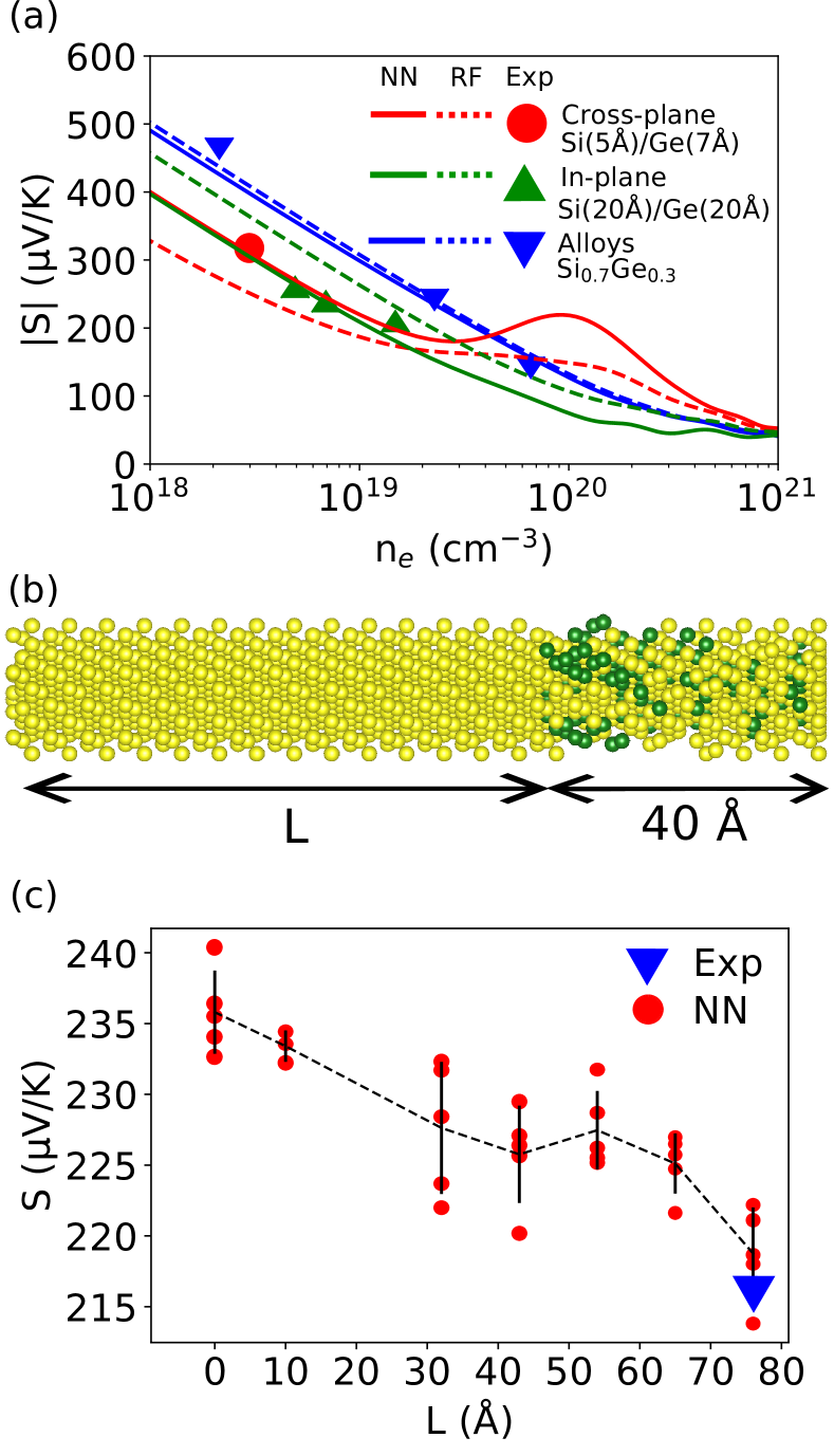
In Fig. 6, we demonstrate the agreement between ML predicted thermopowers (solid (NN) and dashed (RF)) and measured values (circle and triangles) taken from Ref. 59, 60, 18. We chose three system categories to demonstrate the extrapolating power of our ETI framework: -type Si/Ge SLs [18, 59], -type SiGe alloys [60] and -type Si/SiGe SLs [61]. The triangles (green) in Fig. 6(a) represent in-plane thermopowers of -type Si(20Å)/Ge(20Å) SL grown along [001] direction at 300K [18]. We construct our model including 112 Si and 112 Ge atoms, relax the geometry as described in the Methods section, and extract features to obtain the ML prediction. The circle (red) in Fig. 6(a) represents cross-plane thermopower of -type Si(5Å)/Ge(7Å) SL grown along [001] direction at 300K [59]. We extract features from a model Si/Ge SL with 8 Si and 8 Ge atoms to acquire the prediction. The inverted triangles (blue) represent thermopowers of -type Si0.7Ge0.3 alloys at 300K [60], which we model by substituting 19 Si atoms with Ge in a 64-atom bulk Si supercell. The ML predictions show a good agreement for both cross-plane and in-plane thermopowers across all different carrier concentrations. The small deviations between ML results and experimental data can be attributed to the differences between local environments in the models and the experimental samples. We anticipate that the error in ML prediction would fall within experimental uncertainties. This comparison also reveals that ML predictions can be utilized to optimize the thermopowers of these systems by varying carrier concentrations.
In Fig. 6(c), we further establish that the ETI framework can guide heterostructure design with optimized electronic transport properties. We show the NN predicted cross-plane thermopowers of -type Si/SiGe SLs at a carrier concentration cm-3, as a function of varying Si layer thickness (). A representative configuration of a Si/Si0.7Ge0.3 SL is shown in Fig. 6(b). We model systems with a constant width alloy region and varied . As can be noted from the figure that our predictions approach the experimental data obtained for the Si(80Å)/Si0.7Ge0.3(40Å) SL grown on a Si substrate [61] as we approach 80Å. For each system with a given , the spread in ML data refers to five models with different randomized substitutional alloy configurations. Our results establish the remarkable extrapolating power of the framework and also reveal that thermopower of Si/SiGe SLs can be optimized by choosing an appropriate system size guided by ML prediction. We argue that the extension of the prediction domain is enabled by our central hypothesis that local environment-electronic states relationships are preserved across configurations with different compositions. Training ML models with these relationships allows us to predict electronic transport properties of experimental heterostructures. This physics-based extrapolation is thus possible because of accumulating knowledge from “known” environments.
I.4 Scalability of ETI Framework
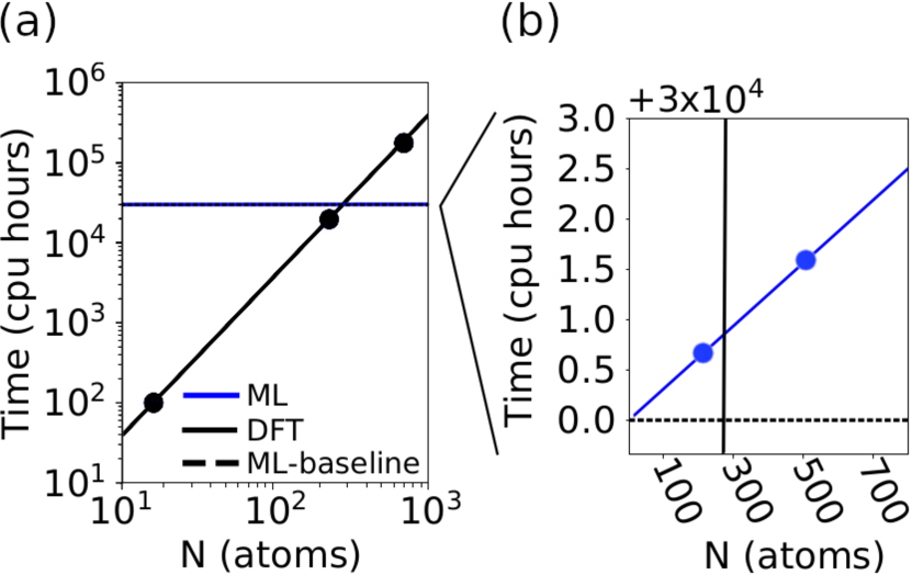
In order to further establish the claim that our ETI framework will help bridge the gap between ab initio accessible and fabricated systems, we explore the scalability of our framework with increasing system size. In Fig. 7, we compare the computational cost of using ETI model to predict electronic properties with direct DFT calculations, with increasing system size. The ML runtime is divided in two parts: the constant baseline, shown by the dashed line in inset of Fig. 7(b) refers to generation of training data with DFT; and the rest is devoted to feature extraction of DFT-relaxed test configurations. The plot shows that runtime for DFT calculations scales as while that for feature extraction scales linearly with , where is number of atoms. Figure 7 establishes the remarkable advantage of the ETI framework for parameter-free prediction of thermopowers of large structures that can not be fully explored with DFT. We acknowledge that identifying the upper bound of this plot would be beneficial but leave it for future work.
In summary, we demonstrate that the problem of predicting electronic properties of technologically relevant heterostructures can be largely solved by combining first-principles methods with ML techniques into a common framework. We illustrate that ML models are capable of extracting information regarding the true interatomic interactions present in ordered (layered) /disordered (alloy) semiconductor structures as a function of variable atomic environment, from the large body of atomistic data generated with individual DFT calculations. We train the ML models on the local environment-electronic state relationships in few-atom fragment units of varied atomic environments, and task the models to predict the environment-state relationships that develop in larger nanostructures, hosting similar local environments. The ML models show remarkable success in predicting thermopowers of experimental heterostructures, validated against experimental data. Our ETI framework establishes a bridge between ideal systems accessible with first-principles approaches and real systems realized with nanofabrication techniques. We elucidate that the extension of the prediction domain is facilitated by a central hypothesis that the local environment-electronic states relationship is preserved across configurations with different global compositions. Our prescription for electronic transport property prediction through codifying correlations in DFT generated electronic structure property data, breaks from previously developed methods that pursued a combinatorics-inspired optimization strategy, especially in the context of thermoelectric materials. Our viewpoint provides a path to extract important physics that determines transport properties of heterostructures, and allows to extend the applicability of first-principles techniques for technologically relevant heterostructures. We anticipate that this viewpoint would give our approach broad applicability to diverse materials classes.
II Methods
II.1 Training and Testing System Details
We model SinGem SLs and “alloys” with different compositions to generate the training data, where and refer to the number of Si and Ge atoms, respectively. We create a fragment unit SinGem () supercell by replicating a 8-atom conventional Si unit cell (CC) twice along the symmetry direction [001] and replacing Si atoms with Ge atoms, since both Si and Ge have stable FCC diamond lattice structures [62, 63]. By replacing Si monolayers (ML) with Ge, we obtain 7 Si8-xGex SLs, where is the number of MLs: . The disordered SiGe structures are prepared with similar 16 atom supercells, two conventional 8-atom cells (CC) stacked along the [001] direction. For each chosen Ge concentration , we generate 50 substitutional “alloy” configurations, resulting in 350 total disordered fragment training units. To generate train and test strained SL structures, we consider applied strains ranging uniformly from to with a total of 7 different strain values, resulting in 49 different SLs, as shown in Fig. 3. We estimate the in-plane strain in the SLs from the lattice constants by [64] with .
The non-ideal heterostructures shown in Fig. 5(b) and Fig. 5(d) are modeled with 32 atom supercells (4 CCs). We construct the model Si(20Å)/Ge(20Å) SL from CCs including 112 Si and 112 Ge atoms and relax the geometry without any applied constraints. We model the Si(5Å)/Ge(7Å) SL shown in Fig. 6(a) with CCs that include 8 Si and 8 Ge atoms. The Si0.7Ge0.3 alloy is modelled using a randomly substituted 64-atom CCs system that includes 45 Si and 19 Ge atoms. The experimental structures shown in Fig. 6(b) are modeled with a SiGe random alloy region ( CCs) and a Si layer of varied lengths between 0 and 10 CCs. We model systems with total size varied from (224 atoms) to CCs (544 atoms) by increasing and keeping the width of the alloy region constant to CCs. For each system with a given , we model the substitutional alloy region with five different randomized configurations.
II.2 DFT Computational Details
The relaxed geometries of the structures are obtained using Vienna Ab Initio Simulation Package (VASP) package. The lattice constants and the atomic positions in SinGem structures are optimized using Broyden-Fletcher-Goldfarb-Shanno Quasi-Newton algorithm, sampling the Brillouin zone (BZ) with -point mesh. To simulate SLs under applied strain, we keep the cell volume fixed and relax the cell shape in every direction. We perform the electronic structure calculations with DFT using the generalized gradient approximation (GGA) implemented in the Vienna Ab initio Simulation Package (VASP) [65, 66] with the Perdew-Burke-Ernzenhof (PBE) exchange-correlation functional [67]. The ultra-soft projector-augmented wave (PAW) pseudopotential [68, 69] with a cutoff energy of 400 eV was used to describe the interaction between the valence electrons and the ions. For the self-consistent calculations, the energy convergence threshold was set to eV. We haven’t included spin-orbit interaction in our analysis since the magnitude of the lattice strain induced splittings is larger than the spin-orbit splittings [70]. The electronic bands are plotted along the symmetry direction of the BZ with 11 points resolution. Following relaxation, we perform non self-consistent field (NSCF) calculations to obtain the band energies using a dense -centered Monkhorst-Pack -point mesh [71], to sample the irreducible Brillouin zone (IBZ). Such sampling is necessary to converge the calculation of the electronic transport coefficients. Once the electronic structure calculations are completed, we employ the semi-classical Boltzmann transport theory [72] as implemented in BoltzTraP code [73] to compute the room temperature Seebeck coefficients. The -point mesh is chosen after systematic studies to converge Seebeck coefficients with increasing the mesh size. In Fig. S8 and S9, we show the convergence of of two representative configurations with increasing the -sampling and number of included bands, respectively.
II.3 Effective Band Structures
Following the approach outlined in Ref. 58, we transform the band structures of larger configurations into EBS of a reference cell consisting of 16 atoms, using spectral decomposition [74]. The reference cell contains the same number of atoms as the training units and is approximately of the same size as 2 CCs stacked along [001] direction. However, the dimensions of the reference cells that each test configuration is projected to are different, and are obtained by dividing the supercells as multiples of 2 CCs and taking an average. We calculate the eigenstates of the test supercells using DFT, sampling the BZ with a -point mesh, where is the band index. The spectral weight that quantifies the amount of character of Bloch states of the reference unit cell preserved in at the same energy , can be written as
| (4) |
The spectral function (SF) can then be defined as
| (5) |
where is a continuous variable of a chosen range over which we probe for the preservation of the Bloch character of the supercell eigenstates. The delta function in Eq. 5 is modeled with a Lorentzian function with width 0.002 eV. are normalized by dividing the spectral functions by .
II.4 Seebeck Coefficients
We compute the Seebeck coefficients using the semi-classical BTE as implemented in the BoltzTraP code [73]. All thermopower calculations are performed at room temperature and for technologically relevant high doping regime ranging from n to cm-3. is obtained from , where is the electron charge, is temperature, and the generalized in-plane () or cross-plane () -order conductivity moments are,
| (6) |
The integrand is computed from the energy difference () to the power, the Fermi energy level (), the derivative of the Fermi-Dirac distribution function () with respect to energy , and the transport distribution function (TDF) [56]. TDF can be expressed as
| (7) |
within the constant relaxation time () approximation. The area-integral is given by the DOS () weighted by the squared group velocities, .
It is known that the PBE-GGA approach poorly predicts semiconductor band gaps [75, 76], as opposed to using hybrid functionals [77]. Nevertheless, the PBE-GGA approximation has been regularly employed to compute the electron/hole transport coefficients of semiconductors, including thermoelectric properties of [111]-oriented Si/Ge SLs [42]. These studies demonstrate the effectiveness of the PBE-GGA approximation to depict the role of lattice environment on electronic properties of Si-based systems. In previous publications, we discussed the discrepancy in bandgap predictions in detail [39] as well as shown comparisons of of Si4Ge4 SLs predicted using the Heyd-Scuseria-Ernzerhof [78] and the PBE functionals [41]. We find that the PBE-predicted vs ne relationship closely follows the HSE prediction for low strain cases, and shows small deviations at low doping concentrations for high strain cases, which can be attributed to bandgap discrepancies [41]. In addition, we tested that using a scissors operator for band gap correction using the HSE predicted gaps (See Ref. 41) or experimental band gap (Fig. S8), essentially leaves the vs ne curve unchanged. This systematic analysis showed the robustness of our results highlighting the relationship between lattice environment and electronic transport in heterostructures, independent of the numerical approach used, and motivated us to use PBE-GGA-BTE approach to analyze the thermopowers of SinGem heterostructures. In the present article, we use a static correction ( eV [42]) to match the PBE predicted band gap to the measured band gap value for bulk silicon. The PBE approach is especially suited for data driven studies since it is far less expensive compared to a more accurate hybrid functional. For example, the electronic bands calculation of a Si4Ge4 SL using PBE, over a -point mesh, required 31 CPU hours and compared to 1075 hours of CPU time when using the hybrid functional.
We used a constant relaxation time () approximation for all the calculations presented in this manuscript. This approximation allows us to calculate without any free parameters. It is a common practice to obtain by fitting experimental mobility data for specific carrier concentrations with empirical approximations, and adjust the first-principle results accordingly to reproduce experimental findings. For example, the first-principles estimation of electronic transport properties of strained bulk Si used relaxation times fitted from the measured mobility data of unstrained Si [42]. One main reason is that first-principles computation of is highly expensive for model systems containing greater than a few atoms. As a result, only a handful of previous studies exist that analyzed the electronic properties of highly technologically relevant Si/Ge heterostructures using first-principle methods, especially with including the complex effects of strain or non-idealities. It is known that strain could alter the dominant scattering processes in bulk Si [79], however, the role of different scattering mechanisms on electron relaxation in Si/Ge heterostructures due to lattice strain or defects is relatively unexplored. In an earlier publication, we estimated the relaxation time assuming that the electron-phonon scattering rates in non-polar semiconductors generally are proportional to the density of states (DOS), and provided a comparison between computed with constant and with [39]. We noted that trends match quite well between the two approximations, although the exact values differ. These observations motivate us to follow a similar approach to compute the electronic transport coefficients in this article. We acknowledge that a detailed analysis of the validity of this approximation would be highly beneficial. However, such a study is out of scope of the present manuscript, especially since our test systems include 100s of atoms. Our aim here is to establish that the local functional relationships present in small models can be harnessed to achieve parameter free prediction of the electronic transport properties of experimental heterostructures. And we have provided a proof of concept by demonstrating that our predictions, made using a constant relaxation time, match the measured data.
III Data availability
The authors declare that the data supporting the findings of this study are available within the main article and the Supplementary Information document.
IV Acknowledgements
The project is funded by the Defense Advanced Research Projects Agency (Defense Sciences Office) [Agreement No.: HR0011-16-2-0043]. This work utilized resources from the University of Colorado Boulder Research Computing Group, which is supported by the National Science Foundation (awards ACI-1532235 and ACI-1532236), the University of Colorado Boulder, and Colorado State University. This work used the Extreme Science and Engineering Discovery Environment (XSEDE), which is supported by National Science Foundation grant number ACI-1548562.
V Author contributions
A.K.P contributed to the acquisition and the analysis of data and the creation of new scripts used in the study; S.N. contributed to the conception and the design of the work, the interpretation of data, drafting and revision of the manuscript.
VI Competing interests
The authors declare no competing interests.
References
- Alferov [2001] Z. I. Alferov, Nobel lecture: The double heterostructure concept and its applications in physics, electronics, and technology, Reviews of modern physics 73, 767 (2001).
- Thompson et al. [2004] S. E. Thompson, M. Armstrong, C. Auth, M. Alavi, M. Buehler, R. Chau, S. Cea, T. Ghani, G. Glass, T. Hoffman, et al., A 90-nm logic technology featuring strained-silicon, IEEE Transactions on Electron Devices 51, 1790 (2004).
- Meyerson [1994] B. S. Meyerson, High-speed silicon-germanium electronics, Scientific American 270, 62 (1994).
- Nissim and Rosencher [2012] Y. Nissim and E. Rosencher, Heterostructures on silicon: one step further with silicon, Vol. 160 (Springer Science & Business Media, 2012).
- Paul [2004] D. J. Paul, Si/sige heterostructures: from material and physics to devices and circuits, Semiconductor science and technology 19, R75 (2004).
- Koester et al. [2006] S. J. Koester, J. D. Schaub, G. Dehlinger, and J. O. Chu, Germanium-on-soi infrared detectors for integrated photonic applications, IEEE Journal of selected topics in quantum electronics 12, 1489 (2006).
- Liu et al. [2010] J. Liu, X. Sun, R. Camacho-Aguilera, L. C. Kimerling, and J. Michel, Ge-on-si laser operating at room temperature, Optics letters 35, 679 (2010).
- Tsaur et al. [1994] B.-Y. Tsaur, C. K. Chen, and S. A. Paul, Heterojunction ge x si 1-x/si infrared detectors and focal plane arrays, Optical engineering 33, 72 (1994).
- Alam and Ramakrishna [2013] H. Alam and S. Ramakrishna, A review on the enhancement of figure of merit from bulk to nano-thermoelectric materials, Nano Energy 2, 190 (2013).
- Taniguchi et al. [2020] T. Taniguchi, T. Ishibe, N. Naruse, Y. Mera, M. M. Alam, K. Sawano, and Y. Nakamura, High thermoelectric power factor realization in si-rich sige/si superlattices by super-controlled interfaces, ACS Applied Materials & Interfaces (2020).
- Shi et al. [2011] Z. Shi, C. Simmons, J. Prance, J. King Gamble, M. Friesen, D. Savage, M. Lagally, S. Coppersmith, and M. Eriksson, Tunable singlet-triplet splitting in a few-electron si/sige quantum dot, Applied Physics Letters 99, 233108 (2011).
- Euaruksakul et al. [2013] C. Euaruksakul, M. M. Kelly, B. Yang, D. E. Savage, G. K. Celler, and M. G. Lagally, Heteroepitaxial growth on thin sheets and bulk material: Exploring differences in strain relaxation via low-energy electron microscopy, Journal of Physics D: Applied Physics 47, 025305 (2013).
- Brehm and Grydlik [2017] M. Brehm and M. Grydlik, Site-controlled and advanced epitaxial ge/si quantum dots: fabrication, properties, and applications, Nanotechnology 28, 392001 (2017).
- Lee et al. [2019] C. Lee, Y.-S. Yoo, B. Ki, M.-H. Jang, S.-H. Lim, H. G. Song, J.-H. Cho, J. Oh, and Y.-H. Cho, Interplay of strain and intermixing effects on direct-bandgap optical transition in strained ge-on-si under thermal annealing, Scientific reports 9, 1 (2019).
- Chen et al. [2013] P. Chen, N. Katcho, J. Feser, W. Li, M. Glaser, O. Schmidt, D. G. Cahill, N. Mingo, and A. Rastelli, Role of surface-segregation-driven intermixing on the thermal transport through planar si/ge superlattices, Physical review letters 111, 115901 (2013).
- David et al. [2018] T. David, J.-N. Aqua, K. Liu, L. Favre, A. Ronda, M. Abbarchi, J.-B. Claude, and I. Berbezier, New strategies for producing defect free sige strained nanolayers, Scientific reports 8, 2891 (2018).
- Samarelli et al. [2013] A. Samarelli, L. Ferre Llin, S. Cecchi, J. Frigerio, T. Etzelstorfer, E. Müller, Y. Zhang, J. Watling, D. Chrastina, G. Isella, et al., The thermoelectric properties of ge/sige modulation doped superlattices, Journal of applied physics 113, 233704 (2013).
- Koga et al. [2000] T. Koga, S. Cronin, M. Dresselhaus, J. Liu, and K. Wang, Experimental proof-of-principle investigation of enhanced z 3d t in (001) oriented si/ge superlattices, Applied Physics Letters 77, 1490 (2000).
- Watling and Paul [2011] J. R. Watling and D. J. Paul, A study of the impact of dislocations on the thermoelectric properties of quantum wells in the si/sige materials system, Journal of Applied Physics 110, 114508 (2011).
- Vargiamidis and Neophytou [2019] V. Vargiamidis and N. Neophytou, Hierarchical nanostructuring approaches for thermoelectric materials with high power factors, Physical Review B 99, 045405 (2019).
- Ramprasad et al. [2017] R. Ramprasad, R. Batra, G. Pilania, A. Mannodi-Kanakkithodi, and C. Kim, Machine learning in materials informatics: recent applications and prospects, npj Computational Materials 3, 1 (2017).
- Schleder et al. [2019] G. R. Schleder, A. C. Padilha, C. M. Acosta, M. Costa, and A. Fazzio, From dft to machine learning: recent approaches to materials science–a review, Journal of Physics: Materials 2, 032001 (2019).
- Snyder et al. [2012] J. C. Snyder, M. Rupp, K. Hansen, K.-R. Müller, and K. Burke, Finding density functionals with machine learning, Physical review letters 108, 253002 (2012).
- Behler [2016] J. Behler, Perspective: Machine learning potentials for atomistic simulations, The Journal of chemical physics 145, 170901 (2016).
- Xia and Kais [2018] R. Xia and S. Kais, Quantum machine learning for electronic structure calculations, Nature communications 9, 1 (2018).
- Gong et al. [2019] S. Gong, T. Xie, T. Zhu, S. Wang, E. R. Fadel, Y. Li, and J. C. Grossman, Predicting charge density distribution of materials using a local-environment-based graph convolutional network, Physical Review B 100, 184103 (2019).
- Ward et al. [2016] L. Ward, A. Agrawal, A. Choudhary, and C. Wolverton, A general-purpose machine learning framework for predicting properties of inorganic materials, npj Computational Materials 2, 1 (2016).
- Meredig et al. [2014] B. Meredig, A. Agrawal, S. Kirklin, J. E. Saal, J. Doak, A. Thompson, K. Zhang, A. Choudhary, and C. Wolverton, Combinatorial screening for new materials in unconstrained composition space with machine learning, Physical Review B 89, 094104 (2014).
- Jain et al. [2016] A. Jain, Y. Shin, and K. A. Persson, Computational predictions of energy materials using density functional theory, Nature Reviews Materials 1, 1 (2016).
- Jain et al. [2013] A. Jain, S. P. Ong, G. Hautier, W. Chen, W. D. Richards, S. Dacek, S. Cholia, D. Gunter, D. Skinner, G. Ceder, and K. a. Persson, The Materials Project: A materials genome approach to accelerating materials innovation, APL Materials 1, 011002 (2013).
- Draxl and Scheffler [2019] C. Draxl and M. Scheffler, The nomad laboratory: From data sharing to artificial intelligence (2019).
- Iwasaki et al. [2019] Y. Iwasaki, I. Takeuchi, V. Stanev, A. G. Kusne, M. Ishida, A. Kirihara, K. Ihara, R. Sawada, K. Terashima, H. Someya, et al., Machine-learning guided discovery of a new thermoelectric material, Scientific reports 9, 1 (2019).
- Hou et al. [2019] Z. Hou, Y. Takagiwa, Y. Shinohara, Y. Xu, and K. Tsuda, Machine-learning-assisted development and theoretical consideration for the al2fe3si3 thermoelectric material, ACS applied materials & interfaces 11, 11545 (2019).
- Xie et al. [2019] T. Xie, A. France-Lanord, Y. Wang, Y. Shao-Horn, and J. C. Grossman, Graph dynamical networks for unsupervised learning of atomic scale dynamics in materials, Nature communications 10, 1 (2019).
- Li et al. [2020] K. Li, J. Lu, and F. Zhai, Neural networks for modeling electron transport properties of mesoscopic systems, Physical Review B 102, 064205 (2020).
- Lopez-Bezanilla and von Lilienfeld [2014] A. Lopez-Bezanilla and O. A. von Lilienfeld, Modeling electronic quantum transport with machine learning, Physical Review B 89, 235411 (2014).
- Nye et al. [1985] J. F. Nye et al., Physical properties of crystals: their representation by tensors and matrices (Oxford university press, 1985).
- Proshchenko et al. [2019a] V. S. Proshchenko, P. P. Dholabhai, T. C. Sterling, and S. Neogi, Heat and charge transport in bulk semiconductors with interstitial defects, Physical Review B 99, 014207 (2019a).
- Proshchenko et al. [2019b] V. S. Proshchenko, M. Settipalli, and S. Neogi, Optimization of seebeck coefficients of strain-symmetrized semiconductor heterostructures, Applied Physics Letters 115, 211602 (2019b).
- Settipalli and Neogi [2020] M. Settipalli and S. Neogi, Theoretical prediction of enhanced thermopower in n-doped si/ge superlattices using effective mass approximation, Journal of Electronic Materials 49, 4431 (2020).
- Proshchenko et al. [2019c] V. Proshchenko, M. Settipalli, A. K. Pimachev, S. Neogi, et al., Modulation of semiconductor superlattice thermopower through symmetry and strain, arXiv preprint arXiv:1907.03461 (2019c).
- Hinsche et al. [2012] N. Hinsche, I. Mertig, and P. Zahn, Thermoelectric transport in strained si and si/ge heterostructures, Journal of Physics: Condensed Matter 24, 275501 (2012).
- Peter and Cardona [2010] Y. Peter and M. Cardona, Fundamentals of semiconductors: physics and materials properties (Springer Science & Business Media, 2010).
- Ridley [1999] B. Ridley, Quantum Processes in Semiconductors (Oxford Univ. Press, 1999).
- Schäffler [1997] F. Schäffler, High-mobility si and ge structures, Semiconductor Science and Technology 12, 1515 (1997).
- Ward et al. [2017] L. Ward, R. Liu, A. Krishna, V. I. Hegde, A. Agrawal, A. Choudhary, and C. Wolverton, Including crystal structure attributes in machine learning models of formation energies via voronoi tessellations, Physical Review B 96, 024104 (2017).
- Ghiringhelli et al. [2015] L. M. Ghiringhelli, J. Vybiral, S. V. Levchenko, C. Draxl, and M. Scheffler, Big data of materials science: critical role of the descriptor, Physical review letters 114, 105503 (2015).
- Xie and Grossman [2018a] T. Xie and J. C. Grossman, Crystal graph convolutional neural networks for an accurate and interpretable prediction of material properties, Physical review letters 120, 145301 (2018a).
- Xie and Grossman [2018b] T. Xie and J. C. Grossman, Hierarchical visualization of materials space with graph convolutional neural networks, The Journal of chemical physics 149, 174111 (2018b).
- Cowley [1950] J. Cowley, An approximate theory of order in alloys, Physical Review 77, 669 (1950).
- Chollet et al. [2015] F. Chollet et al., Keras (2015).
- Breiman and Cutler [2014] L. Breiman and A. Cutler, Random forests, 2001, Mach. Learn 45 (2014).
- Pedregosa et al. [2011] F. Pedregosa, G. Varoquaux, A. Gramfort, V. Michel, B. Thirion, O. Grisel, M. Blondel, P. Prettenhofer, R. Weiss, V. Dubourg, et al., Scikit-learn: Machine learning in python, Journal of machine learning research 12, 2825 (2011).
- Wen et al. [2015] C.-Y. Wen, M. C. Reuter, D. Su, E. A. Stach, and F. M. Ross, Strain and stability of ultrathin ge layers in si/ge/si axial heterojunction nanowires, Nano letters 15, 1654 (2015).
- Gupta et al. [2017] G. Gupta, B. Rajasekharan, and R. J. Hueting, Electrostatic doping in semiconductor devices, IEEE transactions on electron devices 64, 3044 (2017).
- Mahan and Sofo [1996] G. Mahan and J. O. Sofo, The best thermoelectric, Proceedings of the National Academy of Sciences 93, 7436 (1996).
- Popescu and Zunger [2010] V. Popescu and A. Zunger, Effective band structure of random alloys, Physical review letters 104, 236403 (2010).
- Popescu and Zunger [2012] V. Popescu and A. Zunger, Extracting e versus k effective band structure from supercell calculations on alloys and impurities, Physical Review B 85, 085201 (2012).
- Yang et al. [2001] B. Yang, J. Liu, K. Wang, and G. Chen, Characterization of cross-plane thermoelectric properties of si/ge superlattices, in Proceedings ICT2001. 20 International Conference on Thermoelectrics (Cat. No. 01TH8589) (IEEE, 2001) pp. 344–347.
- Dismukes et al. [1964] J. Dismukes, L. Ekstrom, E. Steigmeier, I. Kudman, and D. Beers, Thermal and electrical properties of heavily doped ge-si alloys up to 1300 k, Journal of Applied Physics 35, 2899 (1964).
- Zhang et al. [2002] Y. Zhang, G. Zeng, R. Singh, J. Christofferson, E. Croke, J. E. Bowers, and A. Shakouri, Measurement of seebeck coefficient perpendicular to sige superlattice, in Thermoelectrics, 2002. Proceedings ICT’02. Twenty-First International Conference on (IEEE, 2002) pp. 329–332.
- Pearsall [1991] T. P. Pearsall, Strained-Layer Superlattices: Materials Science and Technology, Vol. 33 (Academic Press, 1991) p. 225.
- Manasreh et al. [1991] M. O. Manasreh, S. T. Pantelides, and S. Zollner, Optoelectronic Properties of Semiconductors and Superlattices, Vol. 15 (Taylor & Francis Books, INC, 1991).
- Van de Walle and Martin [1986] C. G. Van de Walle and R. M. Martin, Theoretical calculations of heterojunction discontinuities in the si/ge system, Physical Review B 34, 5621 (1986).
- Kresse and Furthmüller [1996a] G. Kresse and J. Furthmüller, Efficiency of ab-initio total energy calculations for metals and semiconductors using a plane-wave basis set, Computational materials science 6, 15 (1996a).
- Kresse and Furthmüller [1996b] G. Kresse and J. Furthmüller, Efficient iterative schemes for ab initio total-energy calculations using a plane-wave basis set, Physical review B 54, 11169 (1996b).
- Perdew et al. [1996] J. P. Perdew, K. Burke, and M. Ernzerhof, Generalized gradient approximation made simple, Physical review letters 77, 3865 (1996).
- Kresse and Joubert [1999] G. Kresse and D. Joubert, From ultrasoft pseudopotentials to the projector augmented-wave method, Physical Review B 59, 1758 (1999).
- Blöchl [1994] P. E. Blöchl, Projector augmented-wave method, Physical review B 50, 17953 (1994).
- Hybertsen and Schlüter [1987] M. S. Hybertsen and M. Schlüter, Theory of optical transitions in si/ge (001) strained-layer superlattices, Physical Review B 36, 9683 (1987).
- Monkhorst and Pack [1976] H. J. Monkhorst and J. D. Pack, Special points for brillouin-zone integrations, Physical review B 13, 5188 (1976).
- Ziman [1960] J. M. Ziman, Electrons and phonons: the theory of transport phenomena in solids (Oxford university press, 1960).
- Madsen and Singh [2006] G. K. Madsen and D. J. Singh, Boltztrap. a code for calculating band-structure dependent quantities, Computer Physics Communications 175, 67 (2006).
- Wang et al. [1998] L.-W. Wang, L. Bellaiche, S.-H. Wei, and A. Zunger, “majority representation” of alloy electronic states, Physical review letters 80, 4725 (1998).
- Perdew et al. [2017] J. P. Perdew, W. Yang, K. Burke, Z. Yang, E. K. Gross, M. Scheffler, G. E. Scuseria, T. M. Henderson, I. Y. Zhang, A. Ruzsinszky, et al., Understanding band gaps of solids in generalized kohn–sham theory, Proceedings of the National Academy of Sciences 114, 2801 (2017).
- Morales-García et al. [2017] Á. Morales-García, R. Valero, and F. Illas, An empirical, yet practical way to predict the band gap in solids by using density functional band structure calculations, The Journal of Physical Chemistry C 121, 18862 (2017).
- Hummer et al. [2009] K. Hummer, J. Harl, and G. Kresse, Heyd-scuseria-ernzerhof hybrid functional for calculating the lattice dynamics of semiconductors, Physical Review B 80, 115205 (2009).
- Heyd et al. [2003] J. Heyd, G. E. Scuseria, and M. Ernzerhof, Hybrid functionals based on a screened coulomb potential, Journal of chemical physics 118, 8207 (2003).
- Dziekan et al. [2007] T. Dziekan, P. Zahn, V. Meded, and S. Mirbt, Theoretical calculations of mobility enhancement in strained silicon, Physical Review B 75, 195213 (2007).