Hyper-doped silicon nanoantennas and metasurfaces for tunable infrared plasmonics
Abstract
Abstract.— We present the experimental realization of ordered arrays of hyper-doped silicon nanodisks, which exhibit a localized surface plasmon resonance. The plasmon is widely tunable in a spectral window between 2 and 5 m by adjusting the free carrier concentration between 1020 and 1021 cm-3. We show that strong infrared light absorption can be achieved with all-silicon plasmonic metasurfaces employing nano-structures with dimensions as low as 100 nm in diameter and 23 nm in height. Our numerical simulations show an excellent agreement with the experimental data and provide physical insights on the impact of the nanostructure shape as well as of near-field effects on the optical properties of the metasurface. Our results open highly promising perspectives for integrated all-silicon-based plasmonic devices for instance for chemical or biological sensing or for thermal imaging.
keywords. – Hyper Doped Silicium, Localized Surface Plasmon Resonance, Mid Infrared, Metasurface
Common methods to enhance optical absorption and scattering, and to localize light at subwavelength dimensions are based on either plasmonic Maier et al. (2003) or high refractive index dielectric nanoantennas Kuznetsov et al. (2016) or metasurfaces Genevet et al. (2017).
In the visible spectrum, semiconductor nanostructures tend to receive a growing interest and compete nanostructures of noble metals, thanks to their low losses Kuznetsov et al. (2016); Boltasseva and Atwater (2011) and their direct compatibility with large-scale fabrication techniques from microelectronics.
In the mid-infrared (MIR), in particular at wavelengths ranging from 2 to 15 m, region of interest for chemical or biological sensing and for thermal imaging Tittl et al. (2015, 2018); Fernández-Hurtado et al. (2017); Bareza et al. (2020), those approaches have limitations. For noble metals, it is difficult to support localized surface plasmon resonance (LSPR) in the MIR spectrum, because of their very high free electron concentration (about 1023 cm-3) Luther et al. (2011), or their behavior close to a perfect conductor. Law et al. (2013)
For high index dielectric nanoantennas, the nanostructure dimensions required to send the optical Mie resonances in the MIR are huge (micron size), thus unsuitable for applications such as high resolution infrared detectors requiring a high density of small size pixels.
A promising alternative to enable plasmonics covering a large infrared spectrum are therefore doped semiconductors Li and Ning (2011); Baldassarre et al. (2015); Taliercio and Biagioni (2019), as their LSPR is tunable through the dopant concentration in addition to other parameters such as shape and size Luther et al. (2011). Potential candidates include impurity-doped metal oxides or vacancy-doped copper chalcogenides Kriegel et al. (2017), III-V compounds Law et al. (2014), or germanium. Pellegrini et al. (2018); Baldassarre et al. (2015); Fischer et al. (2016) Though most of these materials supply full compatibility with microelectronics fabrication processes, massively doped silicon (Si) nanostructure arrays are obviously excellent candidates for mass-production of highly integrated low-cost MIR plasmonic devicesNaik et al. (2013).
Carrier concentrations up to a few 1019 cm-3 are common in doped bulk Si. Surface Plasmon Polaritons (SPP) have been demonstrated on and -doped Si layers Ginn et al. (2011); Shahzad et al. (2011), showing improved SPP confinement with respect to metal-dielectric interfaces. However, doping Si nanostructures remains a challenge and is actually far from being mastered. Only few papers report on tunable LSPR in the IR range from doped Si nanostructures. These works involve non-thermal plasma methods and concern free-standing size-distributed nanocrystals, randomly doped at the nanocrystal level.Rowe et al. (2013); Zhou et al. (2015); Kramer et al. (2015)
In this article, we show that the Si overlayer of a Silicon-On-Insulator (SOI) substrate can be massively and homogeneously doped over a wide range of active dopant concentrations, at the state of the art (from 1020 to a few 1021 cm-3). We demonstrate the fabrication of a metasurface composed of dense single crystal Si nanodisks (Si-ND) on silica. We furthermore show that such Si-ND metasurfaces strongly interact with infrared light due to a LSPR, tunable between 2.5 and 5 m, which proves that both the concentration and scattering time of the free carriers are nearly conserved after nanostructuration process. The experimental results are supported by numerical simulations using the Green Dyadic Method (GDM), which allowed us to explore the impact of several parameters on the LSPR, like the exact 3D-shape of the Si nanoantennas, as well as optical near-field interactions in the dense metasurface lattice.
Our top-down approach avoids a statistical distribution of the dopant concentration for hyper-doped Si nanostructures. In a first step, the thin Si overlayer of a SOI is doped by means of a pulsed Laser Thermal Annealing (LTA) melt, a method which has gained recently a considerable interest in microelectronics.Huet et al. (2017); Cristiano et al. (2016) LTA allows reducing the annealing time down to a few tens of nanoseconds while still reaching the melting threshold. In such extremely out-of-equilibrium conditions, concentrations of electrically active dopants beyond the equilibrium solid solubility limit can be achieved in localized regions, while the integrity of the surrounding areas is preserved Huet et al. (2017). The different steps of the elaboration process are summarized in Fig. 1. The starting substrates are SOI wafers with a 23 2 nm nominal thickness (001)-oriented Si overlayer and 20 nm thick SiO2 buried oxide (BOx), lying on an intrinsic Si substrate (See Fig. 1(a)).
Phosphorus (P) is implanted, at low energy (4 keV), in the Si overlayer using four increasing doses (see Table 1). For each dose, only samples corresponding to the optimal LTA conditions are considered for the next process steps, i.e. exhibiting a defect-free single crystal Si (sc-Si) top layer. From those layers, Si-NDs of diameter nm and height 1 nm as measured in Transmission Electron Microscopy (TEM) are obtained by low energy electron beam (e-beam) lithography and reactive-ion etching (RIE) Y Guerfi (2013). The Si-NDs are arranged on a dense hexagonal grid with a periodicity of nm, covering a square area of m2 (see Scanning Electron Miceroscopy image in Fig. 1(b)). Both the Si-ND diameter and lattice periodicity have been chosen to maximize the filling factor of the metasurface (), hence maximizing the light-matter interaction for optical measurements.
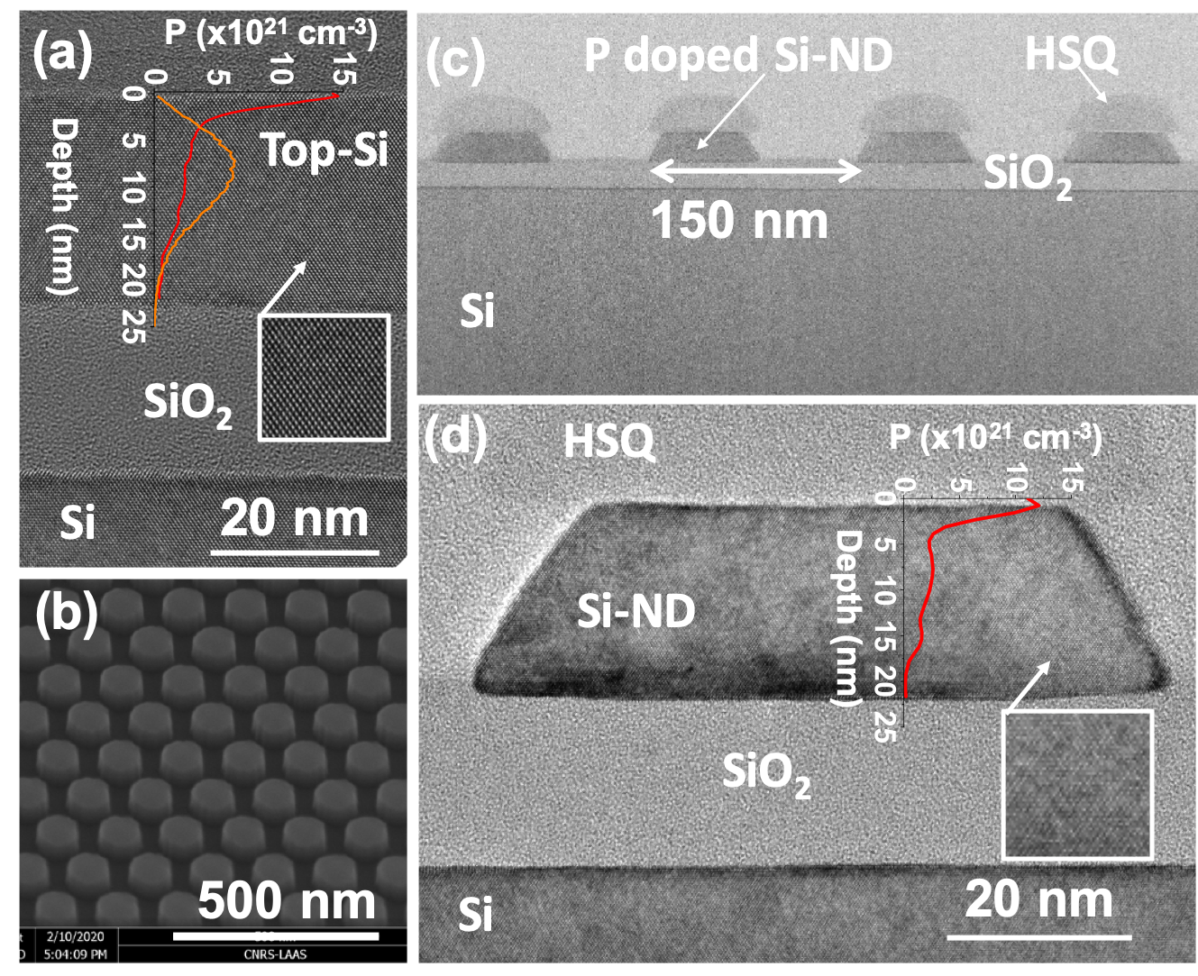
Fig. 1(c) shows a TEM cross-section of several Si-NDs, showing that shape and dimensions are identical, and that a certain amount of under-etching causes a truncated cone shape of the disks. They are covered by a 20 nm Hydrogen Silesquioxane (HSQ) cap, leading to a kind of mushroom shape. The HSQ resist cap is a leftover RIE mask which we is not removed to avoid accidental lift-off of the Si-NDs. All Si-NDs are of identical dimensions and doping level. The latter was evidenced by Scanning TEM - Energy Dispersive X-Ray Spectroscopy (STEM-EDX) measurement of the phosphorus redistribution upon LTA, carried out on several Si-NDs (see P concentration profile, superimposed in Fig. 1(d) and Fig. S1 in Supplementary). A homogeneous P redistribution (plateau) is found in the melted region (Si-ND volume), however with a pile-up of P atoms at the interface of the Si-NDs with the HSQ top layer. The P content in the plateau rises with increasing implanted dose, reaching a saturation value of 2.51021 cm-3 (5 at.). Note that these values are identical to the ones measured in the continuous Si overlayer prior nanostructuration (see Fig. 1(a) and Fig. S1 in Supplementary). This saturation value largely exceeds the solid solubility limit of phosphorus in bulk Si at thermal equilibrium. The pile-up of P at the surface takes place in the annealed SOI layer before nanopatterning and is the result of liquid phase epitaxy of the silicon top layer amorphized by the P implantation. First, during melt, due to dopant diffusivities in the liquid silicon being 108 times greater than in solid silicon, the implanted dopants rapidly redistribute within the melted layer, so that the initial gaussian-like dopant distribution transforms into a much flatter distribution. Then, during solidification, the P atoms are pushed to the melt from solid/liquid interface, i. e. towards the surface, due to the lower solubility of P in solid Si than that in liquid Si Baeri and Rimini (1996); Reitano et al. (1994). This mechanism implies continuous rejection of impurities on the liquid side of the moving interface until, when the total solidification is accomplished, a substantial fraction of the total amount of impurities is accumulated on the surface of the sample.
| Nominal implanted dose D(cm-2) | Nominal concentration (cm-3) | Free carrier density (cm-3) in SOI | Scattering time (fs) | Activation ratio () | |
|---|---|---|---|---|---|
| P1 | (1.8 at.) | – | 6.15–9.22 | 7010 | |
| P2 | (7.2 at.) | – | 4.27–5.64 | 4610 | |
| P3 | (12.5 at.) | – | 3.33–4.61 | 409 | |
| P4 | (18at.) | – | 2.82–3.92 | 3215 |
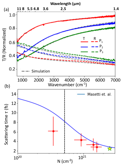
Infrared spectra to quantify the free carrier absorption were measured at room temperature using a Fourier Transform Infrared Spectrometer (FTIR) coupled to a Cassegrain microscope. Fig. 2(a) shows the transmittance and reflectance spectra, recorded on the continuous doped layers for three implanted dopant concentrations P1, P2 and P3 (see Table 1). The transmittance spectra are normalized using a reference, for which the 23 nm thick doped Si overlayer has been completely removed (), allowing the impact of this layer to be determined. Reflectance data are normalized to a thin area of sputtered gold on the same substrate (). The normalized transmittance curves display a value close to unity at high frequency, which strongly decreases at low frequency (below 3000 cm-1). This reduced transmission is linked to light absorption by the free electrons in the -doped layer. As expected, it is associated with a simultaneous increase of the reflectance. As the P concentration increases, obviously linked to an increasing free carrier density, it is evident that the transmittance minimum (resp. reflectance maximum) at low frequency is more pronounced. The transmittance drops to values as low as for sample P3 with the highest concentration.
To extract more quantitative information from our optical measurements, we model the radiative properties of the multilayer structure: doped Si ( nm)/SiO2 ( nm)/intrinsic Si ( m) (Simulations in Fig. 2(a)). The complex refractive index is used to calculate the complex reflectivity and transmissivity for each interface and layer. The radiation inside the film and inside the substrate are treated as coherent and incoherent, respectively. The dielectric functions for SiO2 and intrinsic Si are taken from Chandler-Horowitz and Amirtharaj (2005). The dielectric function of the doped Si layer is described using a Drude-Lorentz model:
| (1) |
where =13 is the value of the dielectric function at high frequency, = the plasma frequency, and the scattering rate. In these expressions, is the electron effective mass in Si, the elementary charge, the free carrier concentration, the scattering time and the electron mobility. Kuzmenko (2005) The free parameters used to fit the experimental data are only and , the other parameters being fixed. For a given phosphorus dose, and are fitted simultaneously Kuzmenko (2005), giving one set of fitting parameters. The dot-dashed black lines in Fig. 2(a) correspond to the best fit for each dose. The fitting lines are nearly indistinguishable from the corresponding experimental transmittance and reflectance curves for all the P doses. This excellent agreement between the experiment and a model taking into account only one Drude term suggests that the active dopant scattering rate (and therefore concentration) is mostly homogeneous (no observable doping gradient), contrary to what has been reported on thicker layers of doped silicon Basu et al. (2010). This indicate that the observed phosphorus piling-up at the interface with the native SiO2 shown by the EDX profile in Fig. 1(f) does not significantly contribute to the optical response of the material.
The extracted free carrier densities displayed in table 1 go from cm-3 for P1 up to cm-3 for P4, exceeding the solid solubility limit and most importantly the electrically active P concentration in bulk Si at thermal equilibrium Pichler (2004) (vertical dashed line in Fig. 2(b)). Our best value nearly reaches the highest reported active P concentration in bulk Si obtained after pulsed laser annealing, with comparable mobilities (star symbol in Fig. 2(b)) Huet et al. (2017). From the free carrier densities we deduced the activation ratio of implanted P ions of 70 for P1, 46 for P2, 40 for P3 and 32 for P4. One can see that not only a large fraction of P is not contributing to the free electron density, but also the activation ratio drops with increasing P concentration.
To determine the impact of the non-activated P fraction on the electronic properties, we compare in Fig. 2(b) scattering time plotted versus the free electron density to the model function developed by Masetti et al.Masetti et al. (1983) () for ideal samples annealed in thermodynamical equilibrium and presenting 100 dopant activation. The agreement suggests that our dopant activation process, while reaching state-of-the-art values, does not dramatically deteriorate the electron mobility and that most, if not all, of the excess P atoms form electrically inactive precipitates.Nobili et al. (1982) Note that the error bars in Fig. 2(b) represent the variations of both mobility and carrier density that can be measured over the laser annealed zone. The uncertainty due to the fitting procedure is significantly smaller.
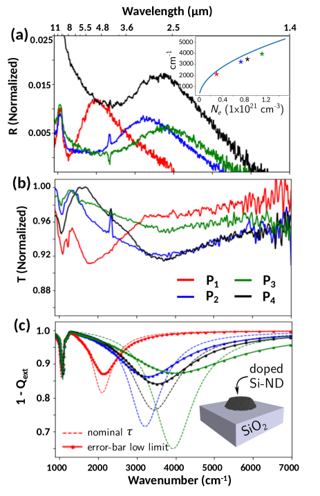
We now investigate the Si-ND metasurfaces with the four P concentrations. Fig. 3(a) and (b) show their reflectance and transmittance spectra. The transmission minima (resp. reflection maxima) no longer appear centered at zero frequency as in the continuous layer case, but are shifted to finite frequency values. Furthermore, the peak shifts towards higher frequency as the free carrier density increases, unambiguously proving that a LSPR is supported by the Si-NDs. The variation of the plasma frequency versus is shown in inset of Fig. 3(a). It displays the typical square root close to the behavior of smaller than the wavelength particle given by:
| (2) |
where is the average dielectric function of the surrounding environment Maier (2007).
The doping range we achieved allows the Si-NDs to interact efficiently with the infrared light over a large spectral range from about 5.5 to 2.5 m. For P1, the LSPR is observed at 1900 cm-1, corresponding to m. The degree of optical field confinement achieved , where is the Si-ND diameter, is comparable, at the same wavelength, to the reduction of the plasmon wavelength in graphene Poumirol et al. (2013); Tamagnone et al. (2018). This is also far better than what can be obtained using noble metals. As a matter of fact, a micron-scale gold stripe would be necessary to support a LSPR at the same energy Law et al. (2013); Liu et al. (2011). Thus, despite the size mismatch between wavelength and Si-NDs, at the plasmon frequency, the metasurface is able to block, either absorb or reflect, around 10 of the incoming light.
To model our experimental results, we performed numerical simulations based on the Green Dyadic Method (GDM) with our homemade simulation toolkit “pyGDM” Wiecha (2018), following the work done by Girard et al. Majorel et al. (2019). This method is based on a volume discretization of the nanostructure and numerical solving of Maxwell’s equations in the frequency domain. From the Lippmann-Schwinger equation
| (3) |
the time Fourier transform of the local electric field is self-consistently obtained at any location, as a function of the incident electric field . The field propagator allows to compute the extinction and scattering efficiencies as well as the near- and far-field radiation patterns of an individual doped Si-ND.Girard et al. (2008)
Please note that the simulations take into account the real dielectric environment (SiO2 substrate), and the real shape of the antennas (a truncated cone with a base diameter of nm and top diameter of nm, as shown in inset of Fig. 3(c)). In order to correctly describe the shape of the nanodisks, the discretization step needs to be small. We use 2454 dipoles on a hexagonal mesh for a Si-ND. As a result of the reduced effective LSPR cavity size, we find that the deviation of the antenna shape from a perfect cylinder causes a 4 redshift of the plasmon frequency.
Fig. 3(c) shows the extinction efficiencies of a single Si-ND on SiO2, using either the average experimental values for the scattering time (dashed lines) or their lower limits from the confidence interval (solid-dot lines, see also Fig. 2(b)). The simulations of the extinction efficiency are in rather good agreement with the corresponding experimental LSPR, reproducing precisely the resonance shift as function of the free carrier concentration. However, while the free carrier concentration determines the spectral position of the LSPR, the width of the resonance is proportional to the damping, hence to the free-carrier scattering rate Khurgin (2015). As can be seen, the lower limits for describe the LSPR broadening much more accurately. This might be an indication that the patterning process reduced the electron mobility in the Si-NDs, which is not surprising as the RIE step may create defects at the Si-ND surfaces.
The single-particle simulations in Fig. 3(c) qualitatively reproduce the extinction, however, the according scattering efficiencies are very low (4-5 orders of magnitude lower than , not shown). The measured reflectance on the other hand is in the order of . To understand the emergence of the relatively pronounced reflectance, we model a hexagonal compact grid of Si-NDs, separated by a 50 nm gap between neighbors, corresponding to the nanodisk distribution on our sample (see inset in Fig. 4(c)). Such a system can per se not be described by the GDM (too many discretization cells). Therefore we use a dipolar effective polarizability approximation for each Si-ND.
The effective polarizability of the truncated cone is extracted as described by Patoux et al.Patoux et al. (2020), and re-injected in the GDM (Eq. 3), in order to calculate the optical response of the plane wave illuminated Si-ND array. The solid lines in Fig. 4(a)-(b) show the calculated reflectance and transmittance spectra, obtained by integration of the energy flux through a plane surface above and below the metasurface and normalization to the respective energy fluxes in the empty environment (without metasurface). The simulations are in very good quantitative agreement with the experimental data. To study the effect of near-field coupling and multiple scattering between the Si-NDs in the dense array, we subsequently switched off artificially the optical near-field interactions between Si-NDs in the simulation (dashed lines in Fig. 4(a)-(b)). We find that the transmittance (resp. the reflectance) is increased (resp. decreased), as a result of near-field coupling compared to the absence of coupling, by about 20 near the LSPR frequency. At the same time, the resonance experiences a slight redshift.
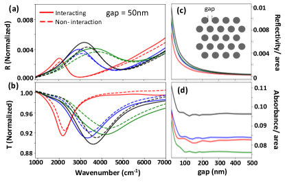
In Fig. 4(c)-(d), we finally show the effect of the lattice periodicity (spacing between the Si-NDs) on the reflectance and absorptance at the LSPR frequency, divided by the nanodisk-covered area. The values are normalized such that the physically correct value is shown for a gap of 50 nm. While the absorptance remains roughly constant and only increases for very small gaps 50 nm, the reflectance strongly increases with decreasing spacing. We observe more than a 10-fold increase in the reflectance per covered area when the spacing goes from 500 nm to 50 nm. At the same time the normalized absorptance remains almost constant. Since near-field coupling causes only about increase of the reflectance for a 50 nm gap (Fig. 4(a)), we attribute the over-proportional enhancement of the reflectance to constructive interference of the scattered light by the individual Si-NDs. This coherent effect offers an additional adjustable parameter to control the metasurface optical properties, since the fine tuning of the lattice periodicity allows to independently adjust the absorptance and reflectance (see Fig. S3 in Supplementary for complete simulated radiation pattern).
In conclusion, by processing hyper-doped overlayers of SOI substrates, we realized all-silicon-based plasmonic metasurfaces formed by submicrometer small doped-Si nanodisks (Si-NDs). We demonstrated that such nanostructures support localized surface plasmon resonances, tunable via the free carrier density of the silicon. State-of-the-Art active dopant concentrations above 1021 cm-3 allow to reach the NIR regime. Despite a huge mismatch between the wavelength (2-5 m) and the Si-ND diameter (nm), the LSPR enables a strong interaction with IR light resulting in a drop of the transmittance of up to 10 at the resonance (see Fig. S4 for performance comparaison with same size gold nanodisk). Via numerical simulations we investigated the optical properties of a single nanodisk as well as of the full metasurface. We identified collective effects and near-field coupling in the metasurface, explaining also its distinct reflectance. Their tunable and high absorptance renders all-silicon-based plasmonic metasurfaces very appealing for applications requiring broadband and high resolution IR detection schemes, such as micro-integrated bolometers or miniaturized IR cameras.
Acknowledgements: This work was partly funded by ANR DONNA (ANR-18-CE09-0034). The authors acknowledge the CALMIP computing facility (grant P12167), the Raimond Castaing characterization platform,the LAAS-CNRS micro and nanotechnologies platform, a member of the French RENATECH network, and SCREEN for the access to the LTA system, C. Bourgerette and S. Pinault (CEMES), F. Carcenac, B. Reig and A. Lecestre (LAAS) for helpful technical support.
References
- Maier et al. (2003) Maier, S. A.; Kik, P. G.; Atwater, H. A.; Meltzer, S.; Harel, E.; Koel, B. E.; Requicha, A. A. G. Local detection of electromagnetic energy transport below the diffraction limit in metal nanoparticle plasmon waveguides. Nature Materials 2003, 2, 229–232.
- Kuznetsov et al. (2016) Kuznetsov, A. I.; Miroshnichenko, A. E.; Brongersma, M. L.; Kivshar, Y. S.; Luk’yanchuk, B. Optically resonant dielectric nanostructures. Science 2016, 354, aag2472.
- Genevet et al. (2017) Genevet, P.; Capasso, F.; Aieta, F.; Khorasaninejad, M.; Devlin, R. Recent advances in planar optics: from plasmonic to dielectric metasurfaces. Optica 2017, 4, 139.
- Boltasseva and Atwater (2011) Boltasseva, A.; Atwater, H. A. Low-Loss Plasmonic Metamaterials. Science 2011, 331, 290–291.
- Tittl et al. (2015) Tittl, A.; Michel, A.-K. U.; Schäferling, M.; Yin, X.; Gholipour, B.; Cui, L.; Wuttig, M.; Taubner, T.; Neubrech, F.; Giessen, H. A Switchable Mid-Infrared Plasmonic Perfect Absorber with Multispectral Thermal Imaging Capability. Advanced Materials 2015, 27, 4597–4603.
- Tittl et al. (2018) Tittl, A.; Leitis, A.; Liu, M.; Yesilkoy, F.; Choi, D.-Y.; Neshev, D. N.; Kivshar, Y. S.; Altug, H. Imaging-based molecular barcoding with pixelated dielectric metasurfaces. Science 2018, 360, 1105–1109.
- Fernández-Hurtado et al. (2017) Fernández-Hurtado, V.; García-Vidal, F. J.; Fan, S.; Cuevas, J. C. Enhancing Near-Field Radiative Heat Transfer with Si-based Metasurfaces. Physical Review Letters 2017, 118.
- Bareza et al. (2020) Bareza, N. J.; Gopalan, K. K.; Alani, R.; Paulillo, B.; Pruneri, V. Mid-infrared Gas Sensing Using Graphene Plasmons Tuned by Reversible Chemical Doping. ACS Photonics 2020, 7, 879–884.
- Luther et al. (2011) Luther, J. M.; Jain, P. K.; Ewers, T.; Alivisatos, A. P. Localized surface plasmon resonances arising from free carriers in doped quantum dots. Nature Materials 2011, 10, 361–366.
- Law et al. (2013) Law, S.; Podolskiy, V.; Wasserman, D. Towards Nano-Scale Photonics with Micro-Scale Photons: The Opportunities and Challenges of Mid-Infrared Plasmonics. Nanophotonics 2013, 2, 103–130, Publisher: De Gruyter Section: Nanophotonics.
- Li and Ning (2011) Li, D.; Ning, C. Z. All-semiconductor active plasmonic system in mid-infrared wavelengths. Optics Express 2011, 19, 14594.
- Baldassarre et al. (2015) Baldassarre, L.; Sakat, E.; Frigerio, J.; Samarelli, A.; Gallacher, K.; Calandrini, E.; Isella, G.; Paul, D. J.; Ortolani, M.; Biagioni, P. Midinfrared Plasmon-Enhanced Spectroscopy with Germanium Antennas on Silicon Substrates. Nano Letters 2015, 15, 7225–7231.
- Taliercio and Biagioni (2019) Taliercio, T.; Biagioni, P. Semiconductor infrared plasmonics. Nanophotonics 2019, 8, 949–990.
- Kriegel et al. (2017) Kriegel, I.; Scotognella, F.; Manna, L. Plasmonic doped semiconductor nanocrystals: Properties, fabrication, applications and perspectives. Physics Reports 2017, 674, 1–52.
- Law et al. (2014) Law, S.; Roberts, C.; Kilpatrick, T.; Yu, L.; Ribaudo, T.; Shaner, E.; Podolskiy, V.; Wasserman, D. All-Semiconductor Negative-Index Plasmonic Absorbers. Physical Review Letters 2014, 112, 017401.
- Pellegrini et al. (2018) Pellegrini, G.; Baldassare, L.; Giliberti, V.; Frigerio, J.; Gallacher, K.; Paul, D. J.; Isella, G.; Ortolani, M.; Biagioni, P. Benchmarking the Use of Heavily Doped Ge for Plasmonics and Sensing in the Mid-Infrared. ACS Photonics 2018, 5, 3601–3607.
- Fischer et al. (2016) Fischer, M. P.; Schmidt, C.; Sakat, E.; Stock, J.; Samarelli, A.; Frigerio, J.; Ortolani, M.; Paul, D. J.; Isella, G.; Leitenstorfer, A.; Biagioni, P.; Brida, D. Optical Activation of Germanium Plasmonic Antennas in the Mid-Infrared. Physical Review Letters 2016, 117, 047401.
- Naik et al. (2013) Naik, G. V.; Shalaev, V. M.; Boltasseva, A. Alternative Plasmonic Materials: Beyond Gold and Silver. Advanced Materials 2013, 25, 3264–3294.
- Ginn et al. (2011) Ginn, J. C.; Jarecki, R. L.; Shaner, E. A.; Davids, P. S. Infrared plasmons on heavily-doped silicon. Journal of Applied Physics 2011, 110, 043110.
- Shahzad et al. (2011) Shahzad, M.; Medhi, G.; Peale, R. E.; Buchwald, W. R.; Cleary, J. W.; Soref, R.; Boreman, G. D.; Edwards, O. Infrared surface plasmons on heavily doped silicon. Journal of Applied Physics 2011, 110, 123105.
- Rowe et al. (2013) Rowe, D. J.; Jeong, J. S.; Mkhoyan, K. A.; Kortshagen, U. R. Phosphorus-Doped Silicon Nanocrystals Exhibiting Mid-Infrared Localized Surface Plasmon Resonance. Nano Letters 2013, 13, 1317–1322.
- Zhou et al. (2015) Zhou, S.; Pi, X.; Ni, Z.; Ding, Y.; Jiang, Y.; Jin, C.; Delerue, C.; Yang, D.; Nozaki, T. Comparative Study on the Localized Surface Plasmon Resonance of Boron- and Phosphorus-Doped Silicon Nanocrystals. ACS Nano 2015, 9, 378–386.
- Kramer et al. (2015) Kramer, N. J.; Schramke, K. S.; Kortshagen, U. R. Plasmonic Properties of Silicon Nanocrystals Doped with Boron and Phosphorus. Nano Letters 2015, 15, 5597–5603.
- Huet et al. (2017) Huet, K.; Mazzamuto, F.; Tabata, T.; Toqué-Tresonne, I.; Mori, Y. Doping of semiconductor devices by Laser Thermal Annealing. Materials Science in Semiconductor Processing 2017, 62, 92–102.
- Cristiano et al. (2016) Cristiano, F.; Shayesteh, M.; Duffy, R.; Huet, K.; Mazzamuto, F.; Qiu, Y.; Quillec, M.; Henrichsen, H.; Nielsen, P.; Petersen, D.; La Magna, A.; Caruso, G.; Boninelli, S. Defect evolution and dopant activation in laser annealed Si and Ge. Materials Science in Semiconductor Processing 2016, 42, 188–195.
- Y Guerfi (2013) Y Guerfi, G. L., F Carcenac High resolution HSQ nanopillar arrays with low energy electron beam lithography” Microelectronic engineering 110, (2013) 173-176. Microelectronic engineering 2013, 173–176.
- Ziegler (2004) Ziegler, J. F. SRIM-2003. Nuclear Instruments and Methods in Physics Research Section B: Beam Interactions with Materials and Atoms 2004, 219-220, 1027–1036.
- Baeri and Rimini (1996) Baeri, P.; Rimini, E. Laser annealing of silicon. Materials Chemistry and Physic 1996, 169–177.
- Reitano et al. (1994) Reitano, R.; Smith, P. M.; Aziz, M. J. Solute trapping of group III, IV, and V elements in silicon by an aperiodic stepwise growth mechanism. Journal of Applied Physics 1994, 76, 1518.
- Masetti et al. (1983) Masetti, G.; Severi, M.; Solmi, S. Modeling of carrier mobility against carrier concentration in arsenic-, phosphorus-, and boron-doped silicon. IEEE Transactions on Electron Devices 1983, 30, 764–769.
- Pichler (2004) Pichler, P. In Intrinsic Point Defects, Impurities, and Their Diffusion in Silicon; Selberherr, S., Ed.; Computational Microelectronics; Springer Vienna: Vienna, 2004.
- Chandler-Horowitz and Amirtharaj (2005) Chandler-Horowitz, D.; Amirtharaj, P. M. High-accuracy, midinfrared refractive index values of silicon. Journal of Applied Physics 2005, 97, 123526.
- Kuzmenko (2005) Kuzmenko, A. B. Kramers–Kronig constrained variational analysis of optical spectra. Review of Scientific Instruments 2005, 76, 083108.
- Basu et al. (2010) Basu, S.; Lee, B. J.; Zhang, Z. M. Infrared Radiative Properties of Heavily Doped Silicon at Room Temperature. Journal of Heat Transfer 2010, 132.
- Nobili et al. (1982) Nobili, D.; Armigliato, A.; Finnetti, M.; Solmi, S. Precipitation as the phenomenon responsible for the electrically inactive phosphorus in silicon. Journal of Applied Physics 1982, 53, 1484–1491.
- Maier (2007) Maier, S. Plasmonics: Fundamentals and applications., springer ed.; 2007; p 67.
- Poumirol et al. (2013) Poumirol, J. M.; Yu, W.; Chen, X.; Berger, C.; de Heer, W. A.; Smith, M. L.; Ohta, T.; Pan, W.; Goerbig, M. O.; Smirnov, D.; Jiang, Z. Magnetoplasmons in Quasineutral Epitaxial Graphene Nanoribbons. Physical Review Letters 2013, 110, 246803.
- Tamagnone et al. (2018) Tamagnone, M.; Slipchenko, T. M.; Moldovan, C.; Liu, P. Q.; Centeno, A.; Hasani, H.; Zurutuza, A.; Ionescu, A. M.; Martin-Moreno, L.; Faist, J.; Mosig, J. R.; Kuzmenko, A. B.; Poumirol, J.-M. Magnetoplasmonic enhancement of Faraday rotation in patterned graphene metasurfaces. Physical Review B 2018, 97, 241410.
- Liu et al. (2011) Liu, X.; Tyler, T.; Starr, T.; Starr, A. F.; Jokerst, N. M.; Padilla, W. J. Taming the Blackbody with Infrared Metamaterials as Selective Thermal Emitters. Physical Review Letters 2011, 107, 045901, Publisher: American Physical Society.
- Wiecha (2018) Wiecha, P. R. pyGDM—A Python Toolkit for Full-Field Electro-Dynamical Simulations and Evolutionary Optimization of Nanostructures. Computer Physics Communications 2018, 233, 167–192.
- Majorel et al. (2019) Majorel, C.; Paillard, V.; Patoux, A.; Wiecha, P. R.; Cuche, A.; Arbouet, A.; Bonafos, C.; Girard, C. Theory of plasmonic properties of hyper-doped silicon nanostructures. Optics Communications 2019, 453, 124336.
- Girard et al. (2008) Girard, C.; Dujardin, E.; Baffou, G.; Quidant, R. Shaping and manipulation of light fields with bottom-up plasmonic structures. New Journal of Physics 2008, 10, 105016.
- Khurgin (2015) Khurgin, J. B. How to deal with the loss in plasmonics and metamaterials. Nature Nanotechnology 2015, 10, 2–6.
- Patoux et al. (2020) Patoux, A.; Majorel, C.; Wiecha, P. R.; Cuche, A.; Muskens, O. L.; Girard, C.; Arbouet, A. Polarizabilities of Complex Individual Dielectric or Plasmonic Nanostructures. Physical Review B 2020, 101, 235418, Publisher: American Physical Society arXiv: 1912.04124.