Programmable Multifunctional Plasmonic Waveguide System based on Coding Metamaterials and Inverse Design
Abstract
In this article, we propose a programmable plasmonic waveguide system (PPWS) to achieve several different functions based on metal coding metamaterials (MCMs) and inverse design technology. There is no need to spend much time on considering the relation between the function and the structure because the MCMs in the PPWS are reprogrammable. In order to demonstrate the effectiveness of the PPWS, we utilize it to achieve several filtering functions, including bandstop and bandpass filters. The simulation results exhibit that the performance of filters is improved based on genetic algorithm, particle swarm optimization, multi-traversal direct-binary search and simulated annealing. Especially, the bandwidth and quality factor for the narrow-band filter can reach 6.5 nm and 200.5. In addition to the simple filtering functions, some relatively complex transmission characteristics can be obtained by using the PPWS, such as plasmon-induced transparency-like effects. In conclusion, genetic algorithm is considered as the most efficient inverse design method for our system due to its less optimization time and stable performance. In comparison with the previous works, our proposed PPWS not only provides a general framework for obtaining an effective, flexible and compact plasmonic device but also shows the applications of inverse design on photonics devices.
keywords:
Plasmonic devices, inverse design, optimization, plasmon-induced transparencyIR,NMR,UV
![[Uncaptioned image]](/html/2011.06800/assets/x1.png)
Table of Contents Entry for Programmable Multifunctional Plasmonic Waveguide System based on Coding Metamaterials and Inverse Design by Yihang Dan, Tian Zhang, Jian Dai, and Kun Xu.
Plasmon-induced transparency-like effect in a metal-dielectric-metal waveguide system is realized based on metal coding metamaterials and inverse design. The metal coding metamaterials marked with green dotted line is optimized by gradient free methods.
1 Introduction
Surface plasmon polaritons (SPPs) are especial electromagnetic waves which occur and propagate at the interface of metal and dielectric and they carry energy and information overcoming the diffraction limit 1. The appearance of SPPs provides a new way to manipulate light at the nanoscale so it is considered to be the most potential way to realize highly integrated optical system in the future 2. Since SPPs are discovered, researchers have studied different ways to excite SPPs, such as grating excitation 3, prism coupling 4, 5, waveguide mode coupling 6, end-fire coupling 7 and local excitation 8. The transmission of SPPs usually depends on special waveguide systems, for example metal-dielectric-metal (MDM) waveguide 9, insulator-metal-insulator waveguide 10, hybrid waveguide 11 and so on. Due to their compact footprint and easy integration, MDM waveguide systems have been widely applied in plasmonic filters 12, 13, splitters 14, 15, optical switches 16, modulators 16, 17, 18, absorbers 19, sensors 20, couplers 21, 22, logic gates 23 and so on. However, in order to realize different functions, researchers often spend much time on searching for and designing the nano-resonators with different shapes 24, 25, 26. For example, the plasmon-induced transparency (PIT) effect 27, 28, which has applications in refractive index sensors and slow light, is a hot spot in the field of SPPs. In order to achieve the PIT effects in the transmission spectrum, various structures of waveguide systems with different resonators have been proposed, such as ring resonators 29, stub resonators 30, T-shaped resonators 31, H-shaped resonators 32, rectangular resonators 33, side-coupled multiple resonators 34, 35, 36, 37 and so on. Obviously, it is cumbersome to construct different resonators for a special purpose. It is expected to improve the design efficiency of photonics devices if there exists a general framework, which can realize multiple functions and avoid repetitive design works. It has been demonstrated that the coding metamaterials, which consist of two types of unit cells, can provide a flexible and controllable platform by using a field-programmable gate array 38. The coding metamaterials are effectively designed to achieve high-performance and easily integrated photonics devices based on the inverse design technology 39, 40, 41, 42. However, it should be noted that the above waveguide systems generally include dielectric coding metamaterials. There are few plasmonic waveguide systems having programmable metal coding metamaterials (MCMs) to obtain multi-functions in a general framework.
The inverse design technology based on optimization algorithms, has been used to search for the appropriate distributions and structure parameter of the MCMs. In general, there are three main ways to implement the inverse design of photonics devices: gradient based methods, gradient free methods and model-based methods 43. As a representative method of thegradient based methods, adjoint variable method (AVM) can optimize for the linear and nonlinear optical devices, but it needs physical background to derive the gradient of objective function 44. Model based methods, such as artificial neural networks (ANNs) and random forests, are also used for the inverse design of photonics devices 45. However, a lot of original data and labels are required to train the model which constructs the physical relationship between the structure parameters and corresponding optical responses. The optimization performance is highly dependent on the effect of pre-training model 46. In comparison to the model-based methods, the gradient free methods, including search strategy and evolution strategy, are simple and effective as they directly search for the optimal solution by iteration and evolution strategies. Genetic algorithm (GA) and particle swarm optimization (PSO) are two representative evolution algorithms, which are inspired by the genetic inheritance and group cooperation 47, 48. Although GA and PSO have been widely applied in the optimization and design of photonic devices 49, 50, 51, 52, 53, 54, 55, 56, they are easy to converge too early and fall into local optimal solution in sometimes. Moreover, simulated annealing (SA) and direct-binary search (DBS) are traditional search algorithms which require less time to converge 56, 57. However, these two algorithms also easily fall into local optimal solution because they are sensitive to the initial states and optimization parameter settings. For specific inverse design tasks with different frameworks, the performance of these algorithms are very different. It is necessary to select the most suitable algorithm according to the actual performance.
In this paper, we propose a programmable plasmonic waveguide system (PPWS) based on MCMs and the inverse design to obtain several different functions. Four optimization algorithms, including GA, PSO, SA and DBS, are used to design for the MCMs in the PPWS to realize multiple optical filtering functions, such as narrowband band stop filter (NBSF), broadband band stop filter (BBSF), narrowband band pass filter (NBPF) and broadband band pass filter (BBPF). The numerical simulation results exhibit that the performance of filters is improved based on the inverse design and weighting operation. For instance, the bandwidth and quality factor of the optimized NBSF can reach 6.5 nm and 200.5, respectively. In addition, some relatively complex transmission characteristics can also be obtained by using the PPWS, for example single plasmon-induced transparency (PIT)-like effect, double PIT-like effects and wavelength-tunable PIT-like effects. In conclusion, GA is considered as the most efficient inverse design method for our system due to less optimization time and stable performance.
2 Device design and simulation results
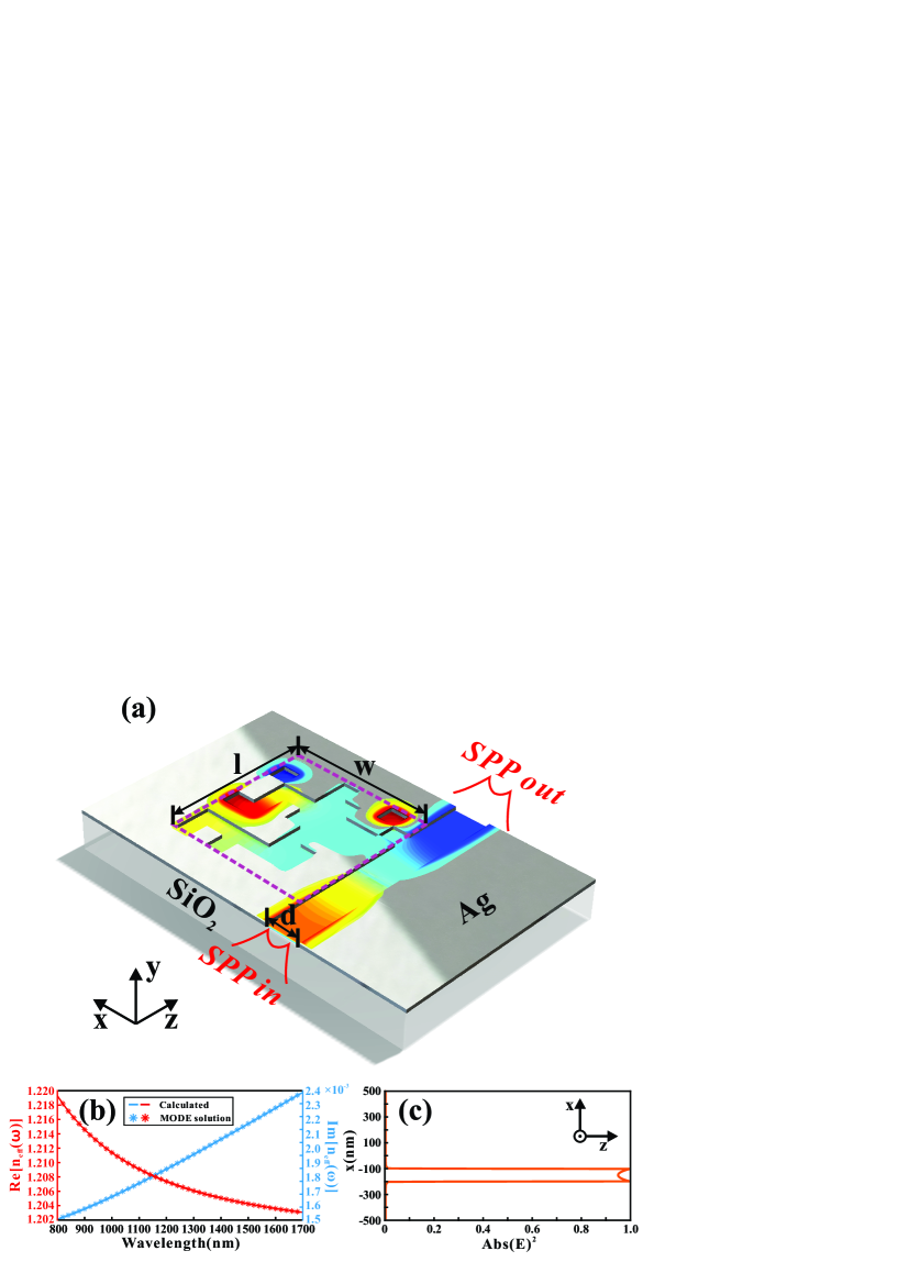
As shown in Fig. 1(a), our proposed PPWS consists of a MDM waveguide and MCMs. The MDM waveguide and MCMs are placed on a SiO2 substrate. Here, the MCMs whose footprint is nm2 and composition is square pixels are placed on one side of the MDM waveguide. Each pixel in the MCMs can be selectively filled by Ag or air, corresponding to the logical state "0" or "1", respectively. Obviously, MCMs provide a relatively broad programming space which is expected to realize different functions based on the inverse design technology. In the PPWS, the length and width of the MDM waveguide which transmits the transverse magnetic (TM) polarized light are 620 nm and 100 nm, respectively. The TM mode in the MDM waveguide can be coupled into the MCMs partially and then be coupled back into the MDM waveguide. The excited modes in the MCMs will have impact on the optical transmission characteristics in the transmission spectrum. In our simulations, the transmission spectrums are calculated by using the 2-dimensional (2D) finite-difference time-domain (FDTD) method (adopting Lumerical FDTD Solutions). The maximum mesh step is set as 1/4 of the length of single pixel in MCMs. The relative dielectric constant of the metal (Ag) in the FDTD simulation is modeled by the Drude model with by the following formula 58:
| (1) |
where is the interband-transition contribution to the permittivity, is the bulk plasma frequency, and is the electron collision frequency. The dispersion relation of the MDM in our system is governed by the following dispersion equation:
| (2) |
where and are the relative dielectric constants of the dielectric and the metal, respectively. is the width of the inner dielectric. and are the transverse propagation constants in the dielectric and the metal, respectively, which are related to the effective refractive index as:
| (3) |
The real part and imaginary part of theoretically calculated and numerically simulated by Lumerical MODE Solutions (which has the same solution in FDTD Solutions) are plotted in Fig. 1(b). The results show that our 2D FDTD simulations is in consistent with theory. Moreover, Fig. 1(c) exhibits the electric field intensity distribution of direction in MDM which is a kind of symmetric TM mode. All the transmission spectrums in our simulations are calculated from 800 nm to 1700 nm in the near infrared region. It should be noted that the MDM waveguide system is usually simulated by using 2D FDTD simulation because of the less simulation time and high accuracy 59, 60, 61. Although the 3D FDTD simulations are more close to the practical devices, their time consumption is relatively high.
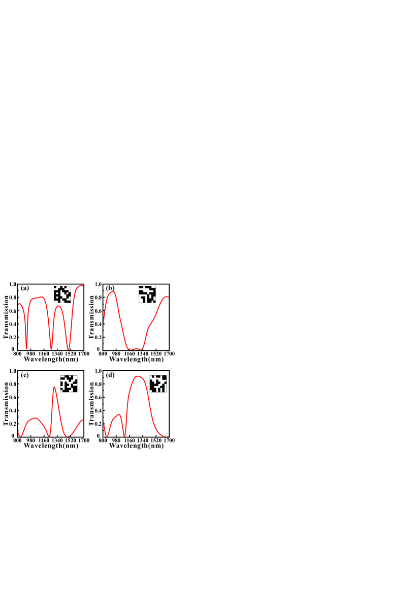
As mentioned above, the PPWS provides a relatively broad programming space to support different functions. In practice, the MCMs can be dynamically controlled by using a field-programmable gate array 38. Here, we randomly select several MCMs to exhibit the transmission characteristics of the PPWS, and the simulation results are shown in Fig. 2. In this simulation, the MCMs whose composition is 88 square pixels reveal that the PPWS has a programming space with 264 distributions although some distributions are senseless and repetitive for one same objective. From Fig. 2(a-d), it can be observed that those transmission spectrums are expected to achieve multi-functional filtering, which is a fundamental and important unit in the integrated plasmonic circuits. And these transmission spectrums are simulated for the MCMs randomly selected from all possible distributions. Obviously, it indicates that the distribution of MCMs could greatly influence the output transmission spectrums and the performance metrics of these filters can be further improved based on the inverse design or optimization algorithms.
3 Multifunctional photonic device
3.1 Multifunctional filter
In section II, we have preliminarily proved that the PPWS has potential as multifunctional filters. It is expected to further improve the performance metrics of the filtering based on the inverse design technology. For example, we want to design a NBSF whose central wavelength and 3dB bandwidth are 1300 nm and 20 nm, respectively. From the beginning, we randomly generate a number of MCMs whose transmission spectrums are simulated by using the 2D FDTD simulation. Then, the MCMs are optimized by using the GA, PSO, SA and DBS to achieve better performance, such as a narrower bandwidth. GA is a highly parallel and adaptive optimization algorithm, which encodes the solutions as genes to achieve evolutionary optimization. Because of the complexity of gene coding, the binary coding, which is suitable for our MCMs, is often used as a simplified substitution 49. The algorithmic details of the GA used here are outlined as follows: (i) an initial population consisted of individuals are randomly generated. Here, each individual in the initial population represents a distribution of MCMs whose pixels are randomly initialized as "0" or "1" state. It should be noted that is an important parameter of the population which has influence on the convergence speed and optimization results. (ii) For all MCMs, the transmission spectrums are calculated by using the 2D FDTD simulation. The Euclidean distance between the simulated transmission spectrum and the targeted transmission spectrum is defined as the optimization objective function (loss) for the GA. And it can determine whether one individual should be eliminated or not in the evolution. Furthermore, the setting of optimization objective function will be discussed in detail as a single part at the end of this section. (iii) A new population are generated by using the selection, crossover and mutation procedures. In the selection process, two parent individuals are selected from previous generation based on the roulette-wheel selection with a gap selection ratio of 0.9 45. In the crossover process, the selected MCMs cross over to generate a new MCMs based on the uniform crossover method with a crossover probability of 0.3. In the mutation process, each pixel in the MCMs has 3% probability to flip from 0 (1) to 1 (0). (iv) The newly generated MCMs are evaluated to determine the GA whether to stop or not. If the genetic generation reaches to 100 or the value of optimization objective function remains unchanged for more than 30 times, then GA stops, otherwise, proceeds to Step (ii).
In comparison to GA, PSO is an evolution algorithm based on group cooperation, which is inspired from the foraging behavior of birds 48. The solution (we call it "particle") of the optimization problem is a "bird" in the search space. All particles have a fitness value determined by the optimization objective function which is the same with GA, and each particle has a velocity that determines the direction and distance for their flight. It should be noticed that the standard PSO is suitable for the decimal problem rather than binary problem so that the discrete binary PSO (DBPSO) rather than the standard PSO is used to optimize the MCMs 62. In the DBPSO, the calculation method for the velocity is as same as the standard PSO. But the velocity of the standard PSO directly affects the position of particle, while that of DBPSO is converted to a flip probability based on the sigmoid function 63. Then, this flip probability determines whether the pixels in the MCMs are changed or not. It should be noted that the velocity range, inertia weight and acceleration constants of the DBPSO in the optimization are set as -11, 1, and 64, respectively. SA is a typical search algorithm which imitates the physical annealing in the quenching based on Monte Carlo iterative solution strategy 65. At the initial stage, SA searches for the solution in a broad optimization space by accepting a worse solution with a certain probability. It can effectively alleviate the local optima problem in the GA and PSO to some extent 66, 67. As the temperature decreases, the solution changes in a small range to speed up the convergence of SA. Here, in each iteration, the MCMs are randomly generated and simulated by the 2D FDTD simulation. The objective function is evaluated to determine the newly generated MCMs whether to be accepted or not with an acceptance probability determined by the Metropolis criterion 68. Here, the maximum and minimum of the temperature for the SA are set as 2000 and 1-18, respectively. And the iteration times for the SA depend on the decrease rate (0.98) of temperature. In addition, DBS is a nonlinear search algorithm which is suitable for discrete binary image 69. From the beginning, each pixel is traversed in turn, and the state with the smaller value of optimization objective function is selected and then fixed each time 57. It should be noticed that the optimal solution will only approach to the direction of convergence in this selection process, so there will be no oscillation and rebound for the value of optimization objective function. Moreover, in order to enhance the performance of PPWS, we increase the time for traversing all pixels. In this article, if the traversal times of the DBS reaches to maximum or the value of loss remains unchanged for more than 10 times, then stopping the search.
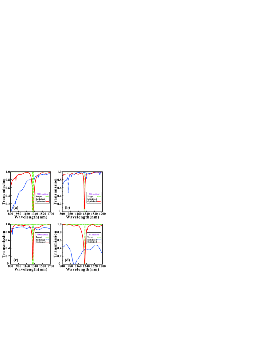
We use GA, DBPSO, SA and DBS to optimize for the MCMs in the PPWS to achieve a NBSF for demonstrating the availability and effectiveness of optimization algorithms. Here, the MCMs in the PPWS are composed of 88 pixels. The targeted central wavelength of the NBSF is set as 1300 nm and the targeted full width at half maximum (FWHM) of the transmission dip is set as 20 nm. Here, the line shape of the targeted transmission spectrum is set as rectangle function. The targeted transmission spectrums (green dash lines) and the optimized transmission spectrums (red solid lines) are shown in Fig. 3. It can be found that the transmission spectrums have a notable improvement after optimizing with four optimization methods since the optimized transmission spectrums are very close to the targeted transmission spectrums comparing with the initial transmission spectrums (blue dash line). Here, the initial transmission spectrums of the DBS and SA are calculated for the initial random distributions of the MCMs, while those of GA and DBPSO are the best individuals in the first generation. After optimizing, we can find that the minimum transmittances of the transmission dips are reduced to 0.0208, 0.0812, 0.1045 and 0.0184 for DBS, GA, DBPSO and SA, respectively. And the central wavelengths (FWHMs) of the optimized NBSFs are 1307.0 nm (7.5 nm), 1299.5 nm (7.5 nm), 1299.0 nm (10.5 nm) and 1303.0 nm (6.5 nm) for DBS, GA, DBPSO and SA, respectively. Correspondingly, the Q-factors of the optimized NBSFs can reach 174.27, 173.67, 123.71 and 200.46, respectively. Obviously, all optimization algorithms are convergent and effective because the optimized transmission spectrums are close to the targeted transmission spectrums. Even so, there exist slight performance differences of the fluctuation degree in the sideband of the optimized transmission spectrums. The max fluctuations of the sideband in the transmission spectrums optimized by the DBS, GA, DBPSO and SA are 2.28 dB, 1.32 dB, 1.48 dB and 0.64 dB, respectively. Though SA has the minimum transmittances and FWHM, which indicates it performs well in this simulation, it is unstable in the optimization process due to the sensitivity of initial condition. GA, by contrast, can get gratifying performance even if it only executes once or twice, which is more stable than others.
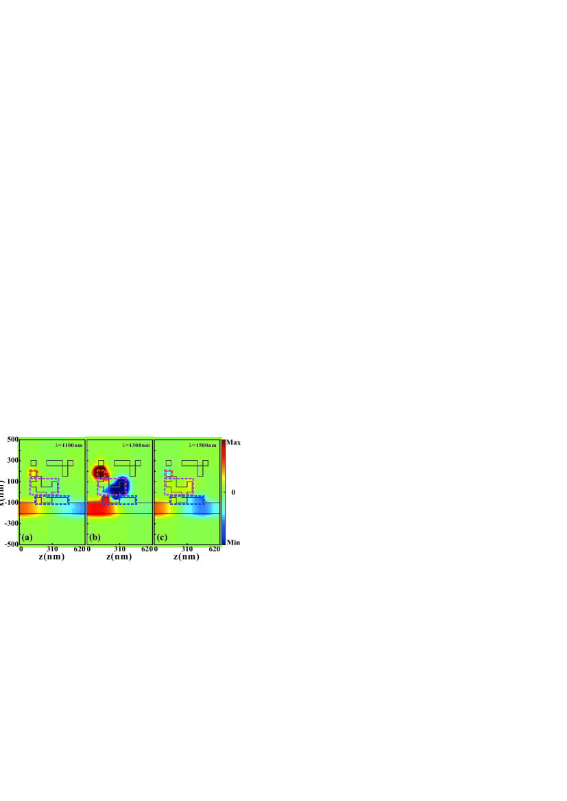
After the optimization, the distribution of the MCMs and the (real part) of the transmission characteristics for NBSF are shown in Fig. 4. The distribution of MCMs comes from the optimization results of DBS method in the Fig. 3. It can be found that for the transmission points at wavelengths 1100 nm and 1500 nm, the SPPs are slightly coupled into MCMs through the pixels surrounded by blue boxes. Obviously, it doesn’t form a stable resonant mode so that SPPs pass through the MDM waveguide with low loss. For the transmission dip at 1300nm, the SPPs are coupled into the MCMs to form a strong resonant mode between the orange zone and magenta zone. Thus, an obvious transmission dip emerges in the transmission spectrum.
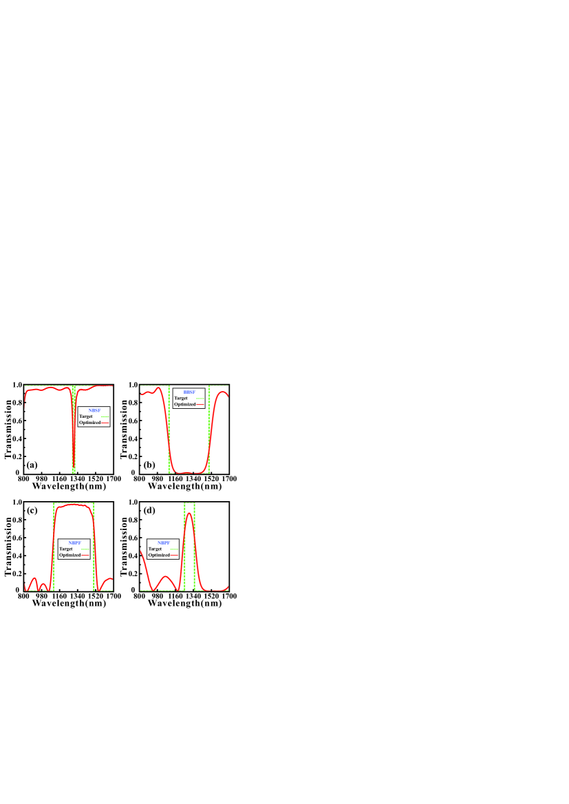
Then, we use GA to optimize for other three types of filters (BBSF, BBPF and NBPF), and corresponding simulation results are shown in Fig. 5. For contrast, the optimized results for the NBSF are shown in Fig. 5(a). Fig. 5(b) shows the optimized transmission spectrum for the BBSF, which has a wide stopband from 1100 nm to 1500 nm. It can be found that the transmittances are less than 0.01 in the stopband and higher than 0.8 in the passband, indicating this BBSF can achieve promising filtering effects. In comparison to the NBSF, the stopband of the BBSF is not enough smooth. The reason for this phenomenon is attributed to the optimized MCMs have redundant pixels, which may lead to the deterioration of performance in the stopband. In addition, Fig. 5(c) shows the optimized transmission spectrum for the BBPF that has a broad passband from 1100 nm to 1500 nm. Here, the maximum transmittance and FWHM of the BBPF reach 0.9718 and 423 nm, respectively. And the maximum fluctuation degree in the passband of the BBPF is only 0.14 dB, which indicates that the passband is very flat. Moreover, we design a NBPF whose 3 dB bandwidth is 133.5 nm, and it’s optimized transmission spectrum is shown in Fig. 5(d). It can be observed that the maximum transmittance of the transmission peak can reach 0.8668 at 1296.5 nm. Obviously, the bandwidth and sideband inhibition of the NBPF can’t be optimized as good as the NBSF. The reason for this phenomenon is related to the loss in the MCMs. In other words, the MCMs is easily used to inhibit rather than promote the transmission of specific wavelengths so that the NBSF have better performance than NBPF. In conclusion, the PPWS is demonstrated to be able to realize multiple optical filtering functions with the remarkable results. And we do not need to make any effort to analysis the resonant mode in the system ahead.
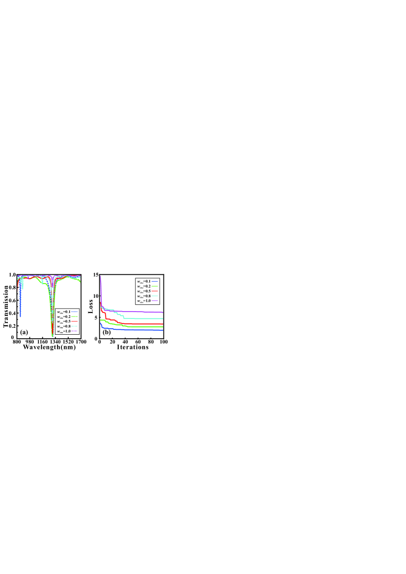
Next, two key elements which have significant influence on the optimal performance of filtering functions are discussed. Firstly, it is clear that the similarity between the simulated transmission spectrum and targeted transmission spectrum determines the performance after optimization. Here, we propose a simple but effective method named "weighting operation" to calculate the similarity for improving the performance metrics. As mentioned above, the Euclidean distances between the simulated transmission spectrums and targeted transmission spectrums are regarded as the optimization objective function (loss). Based on this, we use the weighting factor to calculate the Euclidean distance. The details are outlined as follows: (i) dividing the wavelength range of the transmission spectrums into two parts according to the importance. (ii) One part is called "The central wavelength range (TCWR)", which relates to the wavelength range of stopband or passband we focused on. The other is called "The else wavelength range (TEWR)", which has negligible influence on performance metrics. (iii) In each iteration, the loss is calculated by the following formula:
| (4) |
where is the weighting factor of TCWR, is the weighting factor of TEWR. is the function of calculating Euclidean distance. and represent the simulated transmission spectrum and targeted transmission spectrum in TCWR. While and are the simulated transmission spectrum and targeted transmission spectrum in TEWR.
In order to analyze the influence of the weighting operation, we use GA to optimize for the MCMs in the PPWS to achieve a NBSF. Here, the MCMs are composed of 88 pixels. The targeted central wavelength of the NBSF is set as 1300 nm and the FWHM of the transmission dip is set as 20 nm. TCWR includes the wavelength range from 1290 nm to 1310nm, and the rest of wavelength range belongs to TEWR. The optimized transmission spectrums for different weighting factors of TEWR are shown in Fig. 6(a). After the optimization, we find that the loss values with different weighting factors have a significant decline in Fig. 6(b). The loss values decreases from 3.72 to 1.98 with a 46.77% decline (), 4.35 to 2.77 with a 36.32% decline (), 8.58 to 3.44 with a 59.91% decline (), 7.39 to 4.69 with a 36.54% decline () and 14.69 to 6.14 with a 58.20% decline (), respectively. And the loss value has continuously decline with weighting factor reducing, indicating that the weighting factor has a significant influence on the optimization effects. In Fig. 6(a), it can be found that the minimum transmittance at transmission dip is only 0.7968 when , which is still large for filter even if the loss value has a steep and quick decline in Fig. 6(b). As weighting factor decreases, the minimum transmittance at transmission dip reduces to 0.2389, 0.0812, 0.0376 and 0.0360, respectively. However, it can be observed that the sideband has more violent fluctuations when decreases from 1.0 to 0.1. Besides, the 3dB bandwidths are 14.5 nm, 7.5 nm, 10.5 nm and 8 nm for , , and , respectively. As decreases, the fluctuations in TEWR become more and more strong because the contribution of TEWR becomes smaller. At the same time, the significance of TCWR is amplified equivalently so a small transmittance at transmission dip can be achieved when is decreased. In this article, we use a weighting factor of , which guarantees a balance between bandwidth, minimum transmittance and fluctuations of sideband. Obviously, it is better to dynamically adjust the weighting factor according to the specific application and optimization results of the PPWS.
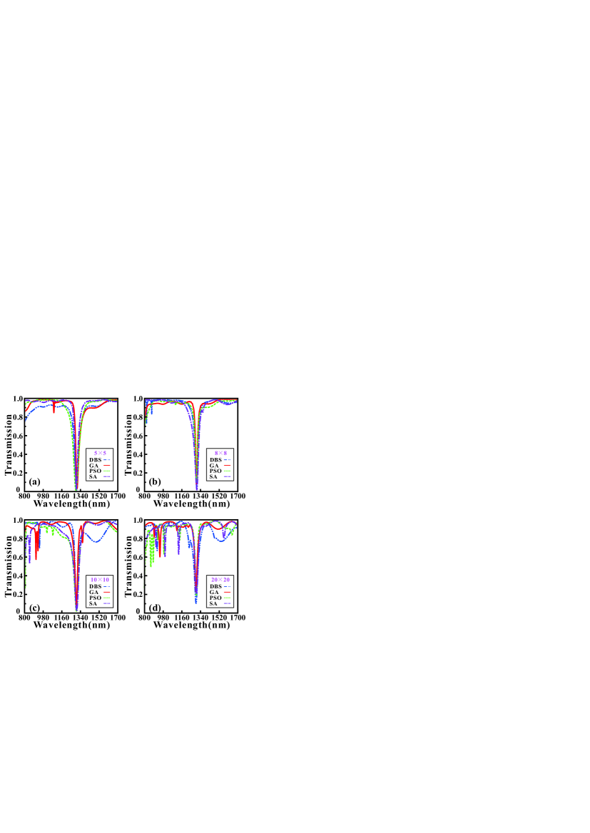
The other key element for the optimization of the PPWS is the density of pixels in MCMs. Obviously, the diversity of MCMs determines the practical functions and performance of the PPWS. Mathematically, the permutation and combination of MCMs grows exponentially as the density of pixels in MCMs increasing. It should be noted that the optimization algorithms we used are suitable for global optimization task but their ability are not infinite. Therefore, it is necessary to choose an appropriate density of pixels in MCMs, which can not only ensure the diversity of MCMs but also maintain the efficiency of the optimization algorithms. In order to analyze the influence of density on the optimization performance, we use all algorithms to optimize for a NBSF with four different densities.
The targeted central wavelength of the NBSF is set as 1300 nm and the FWHM of the transmission dip is set as 20 nm. The optimized transmission spectrums of the NBSF with the MCMs whose densities are pixels, pixels, pixels and pixels are shown in Fig. 7(a)-(d), respectively. The important performance metrics of the optimized transmission spectrums for different densities are exhibited in Table 1. Here, and are the minimum transmittance and the central wavelength of the transmission dip. It can be found that and 3dB bandwidth have remarkable declines as the density of MCMs increases. And the minimum transmittance and 3dB bandwidth for pixels perform the worst in comparison to other densities. It can not be neglected that the fluctuations in the sideband for pixels are extremely violent, which may restrict the applications of filtering function. The reason for this phenomenon is related to that the solution space of pixels is too broad for optimization algorithm to search for the global optimal solution. In addition, it should be noted that the FDTD simulation for high-density MCMs will take much more time to converge as the computational complexity of the high-density MCMs is increased significantly. The choice of density for the MCMs depends on the practical requirements. Moreover, it can be found that the performance differences between pixels, pixels and pixels are not obvious. In comparison to pixels and pixels, the inhibition of the sideband for pixels performs better because it is smoother. The 3dB bandwidth and for pixels are more competitive, but the offset of central wavelength is relatively large, which limits the precise filtering. Considering the diversity and computational efficiency, we select the MCMs with pixels to achieve most of the functionality in this article.
| Density | Method | 3dB bandwidth | ||
|---|---|---|---|---|
| DBS | 1300.5 | 0.0124 | 6.0 | |
| SA | 1299.0 | 0.0267 | 6.5 | |
| DBPSO | 1296.5 | 0.0071 | 6.0 | |
| GA | 1307.0 | 0.0330 | 7.0 | |
| DBS | 1302.5 | 0.0441 | 7.5 | |
| SA | 1303.0 | 0.0184 | 6.5 | |
| DBPSO | 1299.0 | 0.1045 | 10.5 | |
| GA | 1299.5 | 0.0812 | 7.5 | |
| DBS | 1299.5 | 0.0657 | 9.5 | |
| SA | 1302.5 | 0.0185 | 8.0 | |
| DBPSO | 1302.0 | 0.0206 | 8.5 | |
| GA | 1299.5 | 0.0737 | 10.0 | |
| DBS | 1299.5 | 0.1067 | 16.5 | |
| SA | 1302.5 | 0.2064 | 23.5 | |
| DBPSO | 1301.5 | 0.1855 | 13.5 | |
| GA | 1298.5 | 0.2364 | 19.5 |
3.2 PIT-like effect
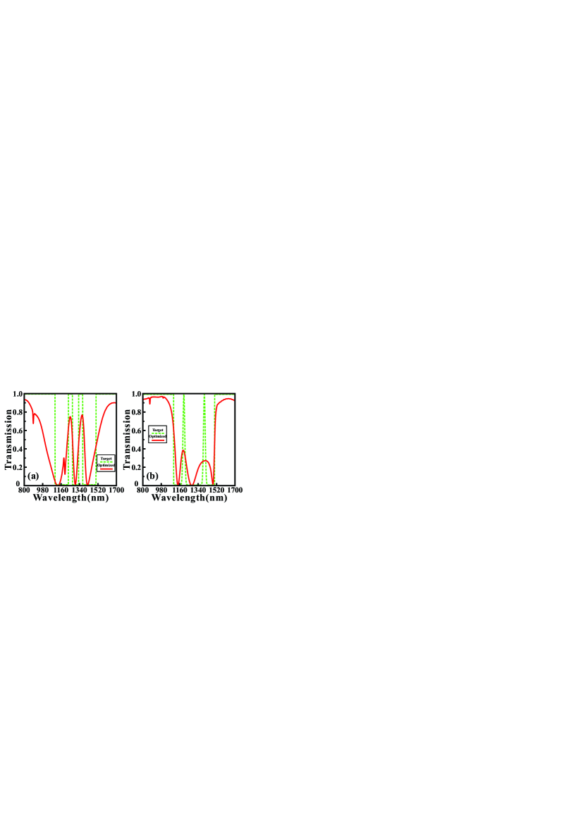
In the previous section, we show that the PPWS can achieve a variety of filtering functions, but these functions are relatively simple. Actually, the PPWS can be programmed to realize advanced functions because of the diversity of MCMs. In addition, this programmable waveguide system can also be used to achieve wavelength-tunable optical devices based on optimization algorithms and the MCMs. Here, we use the GA, whose comprehensive performance is the best in the previous section, to optimize for the MCMs to achieve the PIT-like effects in the transmission spectrum. The optical characteristic of the PIT-like effects includes a transmission peak located between two transmission dips, which has great applications in optical switches, optical data storage and slow light 27, 28. In this FDTD simulation, the MCMs are composed of 88 pixels. The targeted FWHM of the transmission peak is set as 20 nm, while the targeted FWHM of the whole transmission dip is set as 200 nm. The transmission spectrums optimized for the single PIT-like effect are shown in Fig. 8. Obviously, it can be observed that the single PIT-like effect whose center wavelength is 1297 nm is shown in Fig. 8(a), and the targeted central wavelength of the transmission peak is set as 1300 nm. The transmittance of the transmission peak reaches to 0.7115, while the transmittances of the transmission dips are 0.0084 (1251.5 nm) and 0.0086 (1333.5 nm), respectively. As a critical parameter to evaluate the performance of the PIT-like effect, the Q-factor, is calculated by the following formula:
| (5) |
where is the center wavelength of the single PIT-like effect. After the GA optimization, the in Fig. 8(a) is 35.5 nm so that the Q-factor reaches to 36.54. In fact, the Q-factor is lower in the metallic systems due to the ohmic damping 70. What’s more, there is no need to analyze the complex coupling mechanism in a metallic resonator to achieve the single PIT-like effect. In our simulation, we just focus on using efficient optimization algorithms and reasonable physical conditions to obtain the targeted optical characteristics.
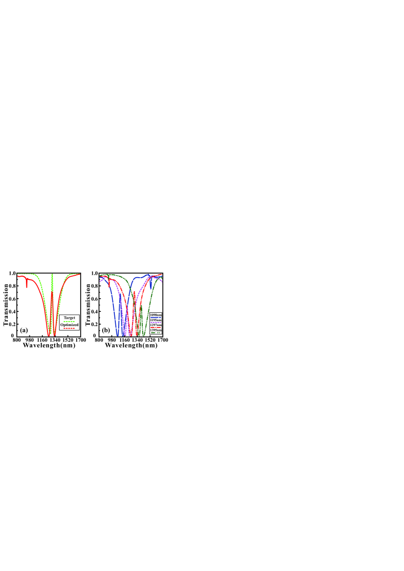
In addition to the PIT-like effects at specific wavelength, the wavelength-tunable PIT-like effects are expected to be applied in highly integrated optical circuits due to flexibility 71, 72. For example, it has been demonstrated that the tunable PIT-like effects can be applied in optical modulators, switches, sensors, slow light and so on 73. Fig. 8(b) shows the wavelength-tunable PIT-like effects based on the PPWS with different central wavelengths. In the optimization process, we only need to adjust the central position of the targeted PIT-like effects and keep other parameters fixed. The center (targeted) wavelengths of the tunable PIT-like effects are 1098 nm (1100 nm), 1195 nm (1200 nm) and 1395 nm (1400 nm), respectively. The maximum deviation between the center wavelength and targeted wavelength is only 5 nm. The corresponding FWHMs (Q-factors) of the tunable PIT- like effects are 31.5 nm (34.86), 27 nm (44.26) and 24 nm (58.13), respectively. And the extinction ratios between the transmission peak and two transmission dips are 22.53 dB (left) and 20.38 dB (right) for the PIT-like effect at 1098 nm, 20.52 dB (left) and 18.93 dB (right) for the PIT-like effects at 1195 nm, 16.55 dB (left) and 18.22 dB (right) for the PIT-like effects at 1395 nm, respectively. Obviously, the FDTD simulation results show that the tunable PIT-like effects can be obtained in the wavelength range from 1100 nm to 1400 nm, which demonstrates that the PPWS has great flexibility and controllability based on the inverse design.
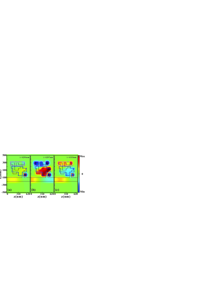
For the single PIT-like effect, the distribution of the MCMs and corresponding electromagnetic field distributions are shown in Fig. 9. Based on the magnetic field distributions, we provide a qualitative explanation for the single PIT-like effect. It can be found that SPPs are confined in these regions which are marked by the yellow rectangular box and red rectangular box, leading to the transmission dips at 1251.5 nm and 1333.5 nm, respectively. For the transmission peak at 1297 nm, SPPs are coupled into yellow zone through the red zone to form a resonant mode. And the phase is same when SPPs are coupled back into the strip waveguide so there is a transmission peak. It should be noted that it is difficult to use the bright-dark mode coupling mechanism or doublet of dressed states to explain the PIT-like effects due to the irregular shapes of MCMs 74.
Finally, we increase the complexity of the targeted transmission spectrum to achieve the double PIT-like effects. The simulated transmission spectrums are shown in Fig. 10. Here, Fig. 10(a) shows an ideal double PIT-like effects with higher transmittances, whose peaks reach to 0.7502 (left channel) and 0.7684 (right channel). By contrast, Fig. 10(b) shows the double PIT-like effects with lower transmittances in the transmission peaks. However, the optimization and matching effects of sideband in Fig. 10(b) are better than those in Fig. 10(a). It should be noted that the sampling points in wavelength range are equidistant in our simulation. But the critical wavelength range that determines the optimization performance is relatively small. Although we use the weighting operation to eliminate the influence from sideband, there still are problems to be solved to make the simulation results match the targeted spectrums perfectly. Even so, it can be observed that the PPWS can be potentially applied to achieve more complex functions from Fig. 9 and Fig. 10.
4 Conclusion
In conclusion, we propose a PPWS based on MCMs and the inverse design. Several optimization algorithms, such as GA, SA, DBS and DBPSO are applied in the design of the MCMs to achieve different functions. The weighting operation can improve the optimization performance. And the FDTD simulation results demonstrate that the optimized PPWS can not only obtain simple functions (such as filters), but also achieve more complex transmission characteristics (for example single PIT-like effect, double PIT-like effects and wavelength-tunable PIT-like effects). Although the perfect matching between the targeted transmission spectrum and optimized transmission spectrum is still difficult to achieve. These results indicate that the PPWS combined with the inverse design has great potential to realize multifunctional plasmonic devices with low cost and high efficiency. There is no need to spend much time on considering the shapes of resonators because the MCMs in the PPWS are reprogrammable. In comparison to the previous works, our proposed PPWS not only provides a general framework for obtaining an effective, flexible and compact plasmonic device but also shows the applications of the inverse design on photonic devices.
This work was supported by the National Natural Science Foundation of China (61705015, 61625104, 61431003, 61821001); Fundamental Research Funds for the Central Universities (2019RC15, 2018XKJC02); National Key Research and Development Program of China (2019YFB1803504, 2018YFB2201803, 2016YFA0301300); Fund of State Key Laboratory of IPOC (BUPT) (NO. IPOC2020ZT08), P. R. China; Beijing Municipal Science and Technology Commission (Z181100008918011).
References
- Cunningham et al. 1974 Cunningham, S.; Maradudin, A.; Wallis, R. Effect of a charge layer on the surface-plasmon-polariton dispersion curve. Phys. Rev. B 1974, 10, 3342–3355
- Zayats et al. 2005 Zayats, A. V.; Smolyaninov, I. I.; Maradudin, A. A. Nano-optics of surface plasmon polaritons. Physics Reports 2005, 408, 131–314
- Hooper and Sambles 2002 Hooper, I.; Sambles, J. Dispersion of surface plasmon polaritons on short-pitch metal gratings. Phys. Rev. B 2002, 65, 836–843
- Otto 1968 Otto, A. Excitation of nonradiative surface plasma waves in silver by the method of frustrated total reflection. Z. Phys. 1968, 216, 398–410
- Kretschmann and Raether 1968 Kretschmann, E.; Raether, H. Notizen: Radiative Decay of Non Radiative Surface Plasmons Excited by Light. Z. Naturforsch. 1968, 23, 2135–2136
- Lavers and Wilkinson 1994 Lavers, C. R.; Wilkinson, J. S. A waveguide-coupled surface-plasmon sensor for an aqueous environment. Sens. Actuators B Chem. 1994, 22, 75–81
- Stegeman et al. 1983 Stegeman, G. I.; Wallis, R. F.; Maradudin, A. A. Excitation of surface polaritons by end-fire coupling. Opt. Lett. 1983, 8, 386–388
- Hecht et al. 1996 Hecht, B.; Bielefeldt, H.; Novotny, L.; Inouye, Y.; Pohl, D. W. Local Excitation, Scattering, and Interference of Surface Plasmons. Phys. Rev. Lett. 1996, 77, 1889–1892
- Kocabaş et al. 2009 Kocabaş, Ş. E.; Veronis, G.; Miller, D. A. B.; Fan, S. Modal analysis and coupling in metal-insulator-metal waveguides. Phys. Rev. B 2009, 79, 035120
- Du et al. 2018 Du, B.; Yang, Y.; Zhang, Y.; Yang, D. Plasmonic Grating Based on Insulator-Metal-Insulator Structure at Telecom Wavelengths. IEEE Photon. Technol. Lett. 2018, 30, 1691–1694
- Hua et al. 2017 Hua, L. U.; Gan, X.; Mao, D.; Zhao, J. Graphene-supported manipulation of surface plasmon polaritons in metallic nanowaveguides. Photo. Res. 2017, 5, 162–167
- Lin and Huang 2008 Lin, X.-S.; Huang, X.-G. Tooth-shaped plasmonic waveguide filters with nanometeric sizes. Opt. Lett. 2008, 33, 2874–2876
- Lu et al. 2010 Lu, H.; Liu, X.; Mao, D.; Wang, L.; Gong, Y. Tunable band-pass plasmonic waveguide filters with nanodisk resonators. Opt. Exp. 2010, 18, 17922–17927
- Kwon et al. 2015 Kwon, M. S.; Shin, J. S.; Lee, J. H. Metal-Insulator-Silicon-Insulator-Metal Waveguide Splitters With Large-Arm Separation. J. Lightw. Technol. 2015, 33, 3843–3849
- Yang et al. 2019 Yang, L.; Li, P.; Li, Z. Plasmonic polarization beam splitting based on single silver nanowire. Opt. Exp. 2019, 27, 3851–3860
- Gómez-Díaz and Perruisseau-Carrier 2013 Gómez-Díaz, J. S.; Perruisseau-Carrier, J. Graphene-based plasmonic switches at near infrared frequencies. Opt. Exp. 2013, 21, 15490–15504
- Emboras et al. 2015 Emboras, A.; Hoessbacher, C.; Haffner, C.; Heni, W.; Koch, U.; Ma, P.; Fedoryshyn, Y.; Niegemann, J.; Hafner, C.; Leuthold, J. Electrically Controlled Plasmonic Switches and Modulators. IEEE J. Sel. Topics Quantum Electron. 2015, 21, 1–8
- Hoessbacher et al. 2017 Hoessbacher, C.; Josten, A.; Baeuerle, B.; Fedoryshyn, Y.; Leuthold, J. Plasmonic modulator with >170 GHz bandwidth demonstrated at 100 GBd NRZ. Opt. Exp. 2017, 25, 1762–1768
- Zhang et al. 2011 Zhang, B.; Zhao, Y.; Hao, Q.; Kiraly, B.; Khoo, I. C.; Chen, S.; Huang, T. J. Polarization-independent dual-band infrared perfect absorber based on a metal-dielectric-metal elliptical nanodisk array. Opt. Exp. 2011, 19, 15221–15228
- Lu et al. 2012 Lu, H.; Liu, X.; Mao, D.; Wang, G. Plasmonic nanosensor based on Fano resonance in waveguide-coupled resonators. Opt. Lett. 2012, 37, 3780–3782
- Ruoxi et al. 2010 Ruoxi,; Yang,; Rami,; A.,; Wahsheh,; Zhaolin,; Lu,; Mustafa,; A.,; and, G. Efficient light coupling between dielectric slot waveguide and plasmonic slot waveguide. Opt. Lett. 2010, 35, 649–651
- Virendra et al. 2019 Virendra,; Patel,; Prateeksha,; Sharma,; V.,; Dinesh,; Kumar, Efficient Coupling From Dielectric to Hybrid Plasmonic Waveguide Using Curved Taper. IEEE Photon. Technol. Lett. 2019, 31, 323–326
- Liu et al. 2019 Liu, Z.; Ding, L.; Yi, J.; Wei, Z.; Guo, J. Design of a multi-bits input optical logic device with high intensity contrast based on plasmonic waveguides structure. Opt. Commun. 2019, 430, 112–118
- Zhang et al. 2014 Zhang, H.; Shen, D.; Zhang, Y. Circular split-ring core resonators used in nanoscale metal–insulator–metal band-stop filters. Laser Phys. Lett. 2014, 11, 115902
- Liu et al. 2017 Liu, X.; Tian, J.; Yang, R. Surface plasmon polariton based metal-insulator-metal filter including two face-to-face concentric semi-rings with different radii. J. Opt. Technol. 2017, 84, 588–592
- Lai et al. 2018 Lai, W.; Wen, K.; Lin, J.; Guo, Z.; Hu, Q.; Fang, Y. Plasmonic filter and sensor based on a subwavelength end-coupled hexagonal resonator. Appl. Opt. 2018, 57, 6369–6374
- Han and Bozhevolnyi 2011 Han, Z.; Bozhevolnyi, S. I. Plasmon-induced transparency with detuned ultracompact Fabry-Perot resonators in integrated plasmonic devices. Opt. Exp. 2011, 19, 3251–3257
- Wang et al. 2012 Wang, G.; Lu, H.; Liu, X. Dispersionless slow light in MIM waveguide based on a plasmonic analogue of electromagnetically induced transparency. Opt. Exp. 2012, 20, 20902–20907
- Zhan et al. 2014 Zhan, S.; Li, H.; Cao, G.; He, Z.; Li, B.; Yang, H. Slow light based on plasmon-induced transparency in dual-ring resonator-coupled MDM waveguide system. J. Phys. D, Appl. Phys. 2014, 47, 205101
- Chen et al. 2012 Chen, J.; Wang, C.; Zhang, R.; Xiao, J. Multiple plasmon-induced transparencies in coupled-resonator systems. Opt. Lett. 2012, 37, 5133–5135
- Lu et al. 2011 Lu, H.; Liu, X.; Mao, D.; Gong, Y.; Wang, G. Induced transparency in nanoscale plasmonic resonator systems. Opt. Lett. 2011, 36, 3233–3235
- Chen et al. 2018 Chen, H.; Zhang, H.; Guo, X.; Liu, S.; Zhang, Y. Tunable plasmon-induced transparency in H-shaped Dirac semimetal metamaterial. Appl. Opt. 2018, 57, 752–756
- Han et al. 2015 Han, X.; Wang, T.; Li, X.; Liu, B.; He, Y.; Tang, J. Ultrafast and Low-Power Dynamically Tunable Plasmon-Induced Transparencies in Compact Aperture-Coupled Rectangular Resonators. J. Lightw. Technol. 2015, 33, 3083–3090
- Guo 2014 Guo, J. Plasmon-induced transparency in metal-insulator-metal waveguide side-coupled with multiple cavities. Appl. Opt. 2014, 53, 1604–1609
- Liu et al. 2015 Liu, H.; Ren, G.; Gao, Y.; Lian, Y.; Qi, Y.; Jian, S. Tunable subwavelength terahertz plasmon-induced transparency in the InSb slot waveguide side-coupled with two stub resonators. Appl. Opt. 2015, 54, 3918–3924
- Lu et al. 2012 Lu, H.; Liu, X.; Mao, D. Plasmonic analog of electromagnetically induced transparency in multi-nanoresonator-coupled waveguide systems. Phys. Rev. A 2012, 85, 053803
- He et al. 2014 He, Z.; Li, H.; Zhan, S.; Cao, G.; Li, B. Combined theoretical analysis for plasmon-induced transparency in waveguide systems. Opt. Lett. 2014, 39, 5543–5546
- Cui et al. 2014 Cui, T. J.; Qi, M. Q.; Wan, X.; Zhao, J.; Cheng, Q. Coding metamaterials, digital metamaterials and programmable metamaterials. Light Sci. Appl. 2014, 3, e218
- Jia et al. 2018 Jia, H.; Zhou, T.; Fu, X.; Ding, J.; Yang, L. Inverse-Design and Demonstration of Ultracompact Silicon Meta-Structure Mode Exchange Device. Amer. Chem. Soc. Photon. 2018, 5, 1833–1838
- Shen et al. 2015 Shen, B.; Polson, R.; Menon, R. Broadband asymmetric light transmission via all-dielectric digital metasurfaces. Opt. Exp. 2015, 23, 20961–20970
- Xie et al. 2020 Xie, Z.; Lei, T.; Qiu, H.; Zhang, Z.; Wang, H.; Yuan, X. Broadband on-chip photonic spin Hall element via inverse design. Photo. Res. 2020, 8, 121–126
- Wang et al. 2020 Wang, K.; Ren, X.; Chang, W.; Lu, L.; Liu, D.; Zhang, M. Inverse design of digital nanophotonic devices using the adjoint method. Photon. Res. 2020, 8, 528–533
- Molesky et al. 2018 Molesky, S.; Lin, Z.; Piggott, A. Y.; Jin, W.; Vuckovic, J.; Rodriguez, A. W. Inverse design in nanophotonics. Nature Photon. 2018, 12, 659–670
- Hughes et al. 2018 Hughes, T. W.; Minkov, M.; Williamson, I. A. D.; Fan, S. Adjoint Method and Inverse Design for Nonlinear Nanophotonic Devices. Amer. Chem. Soc. Photon. 2018, 5, 4781–4787
- Zhang et al. 2019 Zhang, T.; Wang, J.; Liu, Q.; Zhou, J.; Dai, J.; Han, X.; Zhou, Y.; Xu, K. Efficient spectrum prediction and inverse design for plasmonic waveguide systems based on artificial neural networks. Photo. Res. 2019, 7, 368–380
- Liu et al. 2018 Liu, D.; Tan, Y.; Khoram, E.; Yu, Z. Training Deep Neural Networks for the Inverse Design of Nanophotonic Structures. Amer. Chem. Soc. Photon. 2018, 5, 1365–1369
- Holland 1992 Holland, J. H. Adaptation in Natural and Artificial Systems: An Introductory Analysis with Applications to Biology, Control, and Artificial Intelligence; MIT Press, 1992
- Kennedy and Eberhart 2002 Kennedy, J.; Eberhart, R. C. Particle swarm optimization. 2002, 4, 1942–1948
- Skaar and Risvik 1998 Skaar, J.; Risvik, K. M. A genetic algorithm for the inverse problem in synthesis of fiber gratings. J. Lightw. Technol. 1998, 16, 1928–1932
- Kern and Werner 2003 Kern, D. J.; Werner, D. H. A genetic algorithm approach to the design of ultra-thin electromagnetic bandgap absorbers. Microw. Opt. Technol. Lett. 2003, 38, 61–64
- Chen et al. 2008 Chen, P.; Chen, C.; Wang, H.; Tsai, J. H.; Ni, W. Synthesis design of artificial magnetic metamaterials using a genetic algorithm. Opt. Exp. 2008, 16, 12806–12818
- Zhang et al. 2020 Zhang, T.; Xie, J.; Dan, Y.; Yu, S.; Han, X.; Dai, J.; Xu, K. Efficient Optical Spatial First-Order Differentiator Based on Graphene-Based Metalines and Evolutionary Algorithms. IEEE Photon. J. 2020, 12, 1–10
- Shokoohsaremi and Magnusson 2007 Shokoohsaremi, M.; Magnusson, R. Particle swarm optimization and its application to the design of diffraction grating filters. Opt. Lett. 2007, 32, 894–896
- Forestiere et al. 2010 Forestiere, C.; Donelli, M.; Walsh, G. F.; Zeni, E.; Miano, G.; Dal Negro, L. Particle-swarm optimization of broadband nanoplasmonic arrays. Opt. Lett. 2010, 35, 133–135
- Lu et al. 2018 Lu, Q.; Wei, W.; Yan, X.; Shen, B.; Luo, Y.; Zhang, X.; Ren, X. Particle swarm optimized ultra-compact polarization beam splitter on silicon-on-insulator. Photon. Nanostr. Fundam. Appl. 2018, 32, 19–23
- Kim and O’Brien 2004 Kim, W. J.; O’Brien, J. D. Optimization of a two-dimensional photonic-crystal waveguide branch by simulated annealing and the finite-element method. J. Opt. Soc. Am. B 2004, 21, 289–295
- Shen et al. 2015 Shen, B.; Wang, P.; Polson, R.; Menon, R. An integrated-nanophotonics polarization beamsplitter with 2.42.4 footprint. Nature Photon. 2015, 9, 378–382
- Johnson and Christy 1972 Johnson, P. B.; Christy, R. W. Optical Constants of the Noble Metals. Phys. Rev. B 1972, 6, 4370–4379
- Cao et al. 2013 Cao, G.; Li, H.; Zhan, S.; Xu, H.; Liu, Z.; He, Z.; Wang, Y. Formation and evolution mechanisms of plasmon-induced transparency in MDM waveguide with two stub resonators. Opt. Exp. 2013, 21, 9198–9205
- Zhan et al. 2016 Zhan, S.; Peng, Y.; He, Z.; Li, B.; Chen, Z.; Xu, H.; Li, H. Tunable nanoplasmonic sensor based on the asymmetric degree of Fano resonance in MDM waveguide. Sci. Rep. 2016, 6, 22428–22428
- Pannipitiya et al. 2010 Pannipitiya, A.; Rukhlenko, I. D.; Premaratne, M.; Hattori, H. T.; Agrawal, G. P. Improved transmission model for metal-dielectric-metal plasmonic waveguides with stub structure. Opt. Exp. 2010, 18, 6191–6204
- Kennedy and Eberhart 1997 Kennedy, J.; Eberhart, R. C. A discrete binary version of the particle swarm algorithm. 1997, 5, 4104–4108
- Chuang et al. 2008 Chuang, L.; Chang, H.; Tu, C.; Yang, C. Improved binary PSO for feature selection using gene expression data. Comput. Biol. Chem. 2008, 32, 29–38
- Eberhart and Shi 2000 Eberhart, R. C.; Shi, Y. Comparing inertia weights and constriction factors in particle swarm optimization. 2000, 1, 84–88
- Laarhoven and Aarts 1987 Laarhoven, P. J. M.; Aarts, E. H. L. Simulated Annealing: Theory and Applications; Kluwer Academic Publishers: USA, 1987
- Jamili et al. 2011 Jamili, A.; Shafia, M. A.; Tavakkolimoghaddam, R. A hybrid algorithm based on particle swarm optimization and simulated annealing for a periodic job shop scheduling problem. J. Adv. Manuf. Technol. 2011, 54, 309–322
- Yu et al. 2000 Yu, H.; Fang, H.; Yao, P.; Yuan, Y. A combined genetic algorithm:simulated annealing algorithm for large scale system energy integration. Comput. Chem. Eng. 2000, 24, 2023–2035
- Kirkpatrick et al. 1983 Kirkpatrick, S.; Gelatt, C. D.; Vecchi, M. P. Optimization by Simulated Annealing. Science 1983, 220, 671–680
- Seldowitz et al. 1987 Seldowitz, M. A.; Allebach, J. P.; Sweeney, D. W. Synthesis of digital holograms by direct binary search. Appl. Opt. 1987, 26, 2788–2798
- Hu et al. 2018 Hu, J.; Lang, T.; Hong, Z.; Shen, C.; Shi, G. Comparison of Electromagnetically Induced Transparency Performance in Metallic and All-Dielectric Metamaterials. J. Lightw. Technol. 2018, 36, 2083–2093
- Han et al. 2015 Han, X.; Wang, T.; Li, X.; Xiao, S.; Zhu, Y. Dynamically tunable plasmon induced transparency in a graphene-based nanoribbon waveguide coupled with graphene rectangular resonators structure on sapphire substrate. Opt. Exp. 2015, 23, 31945–31955
- Zhang et al. 2017 Zhang, T.; Dai, J.; Dai, Y.; Fan, Y.; Han, X.; Li, J.; Yin, F.; Zhou, Y.; Xu, K. Tunable Plasmon Induced Transparency in a Metallodielectric Grating Coupled With Graphene Metamaterials. J. Lightw. Technol. 2017, 35, 5142–5149
- Wang et al. 2015 Wang, G.; Zhang, W.; Gong, Y.; Liang, J. Tunable Slow Light Based on Plasmon-Induced Transparency in Dual-Stub-Coupled Waveguide. IEEE Photon. Technol. Lett. 2015, 27, 89–92
- Wang et al. 2014 Wang, T.; Zhang, Y.; Hong, Z.; Han, Z. Analogue of electromagnetically induced transparency in integrated plasmonics with radiative and subradiant resonators. Opt. Exp. 2014, 22, 21529–21534