Highly tunable layered exciton in bilayer WS2: linear quantum confined Stark effect versus electrostatic doping
Abstract
Keywords: 2D materials, transition metal dichalcogenide, excitonic reflection, absorption, spectral tuning, electric field, oscillator strength.
The ultra-fast radiative recombination rate 1, 2, 3 of the strongly bound excitons 4, 5, 6 in monolayer transition metal dichalcogenides (TMDCs) leads to efficient photoemission 7, 8. The fast re-radiation of the absorbed photon by the exciton without ample opportunity to suffer from non-radiative processes results in near perfect excitonic reflectance 9, 10, 11. On the other hand, in a bilayer TMDC, a lower indirect energy bandgap appears while the direct energy gap at the point of the Brillouin zone is maintained. This causes the momentum-direct excitons in bilayer to encounter strong non-radiative processes 12, and thus a bilayer TMDC is weakly luminescent 13, while still exhibiting strong excitonic absorption.
To be able to tune the excitonic absorbtion in a dynamic manner is crucial to multiple applications such as programmable optical modulators, tunable photodetectors, optical computing and imaging, laser pulse shaping, and ultra-light optomechanical mirrors. A bilayer distinguishes itself from the monolayers in a number of ways in terms of tunability of the exciton oscillator strength and its spectral control. First, the reflection symmetry along the c-axis is present in a monolayer TMDC, but is broken in a bilayer. Thus, in presence of a vertical electric field, one expects that a bilayer would show linear Stark shift, in contrast to a quadratic one 14, 15, 16, 17 in monolayer. In spite of theoretical predictions of linear quantum confined Stark effect (QCSE) in bilayer TMDC 18, 19, 20, 21, 22, 23, 24, 25, there has not been any experimental demonstration of the same to date for the direct intra-layer exciton. Second, the presence of two layers in a bilayer, which are rotated at with respect to each other, offers an additional layer degree of freedom 12. With a vertical electric field, there is a possibility to convert the intra-layer exciton at zero field to an inter-layer exciton, resulting in a strong tunability of the oscillator strength. Third, it is easier to inject carriers in a bilayer from a metal contact due to reduced bandgap, increased valley degeneracy and enhanced orbital coupling to metal 26. This allows fast and efficient modulation of the excitonic oscillator strength by inter-conversion between a neutral exciton and a charge exciton (trion) through electrostatic doping 27, 28, 29.
In this work we use two different device structures to segregate the effects of electric field induced QCSE and electrostatically induced doping on both the strength and the spectral tunability of the excitonic response in a bilayer WS2. We use a few-layer graphene (FLG)/hBN/2L-WS2/hBN/FLG stack keeping the bilayer WS2 electrically floating to report linear QCSE of the direct intra-layer exciton. The corresponding excitonic oscillator strength is shown to exhibit a large tunability due to an electric field driven partial inter-conversion between intra-layer and inter-layer exciton. We further demonstrate that placing a graphene layer right under the bilayer WS2 is promising for an atomically thin, gate tunable electro-absorption layer. To demonstrate the electrostatically induced doping effect, we use a similar stack, but with the bilayer WS2 connected to a grounded metal contact. The efficient carrier injection from the contact leads to effective oscillator strength transfer from neutral exciton to positive or negatively charged trions depending on the polarity of the gate voltage.
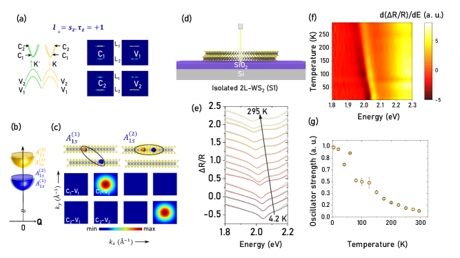
In the 2H form of bilayer WS2, the individual layers are rotated by 180∘ with respect to each other, making the unit cell inversion symmetric. This requires an additional layer degree of freedom () to describe excitons in bilayer for a given spin () and valley (). To describe the lowest energy excitonic states in a bilayer, we use a simple quasiparticle Hamiltonian using tungsten orbitals as the basis functions 30, 12 and solve the Bethe-Salpeter (BS) equation31, 12, as described in Supporting Information 1. As an example, in Figure 1a, we schematically illustrate the lowest energy conduction and valence bands for one of the degenerate cases () along with the layer distribution of the wave functions close to point. The energy dispersion of lowest energy excitonic states with center of mass momentum () is schematically depicted in Figure 1b. The calculated -space distribution of the excitonic state with is depicted in Figure 1c. Depending on the layer distribution of the single particle wave functions, we have both intra-layer [] and inter-layer [] 1s excitons, with the latter being the lowest energy one for bilayer WS2. The layer index of the intra-layer exciton is coupled with spin and valley such that =.= 12, which results in two degenerate configurations for each at zero external field. While radiative recombination is allowed for both these types of excitons by standard selection rules, the intra-layer exciton exhibits more than an order of magnitude higher radiative decay rate compared with the inter-layer exciton 12, and hence the optical response in bilayer discussed here is dominated by the intra-layer exciton 32. The inter-layer exciton noted above is momentum-direct with 12, 33, 34, 35, 36, which is distinct from the indirect inter-layer exciton 37, 38. Due to the difference in spin splitting of the bright and the dark states in Mo and W-based TMDCs, the inter-layer exciton is energetically above the intra-layer exciton in MoTe2 33, MoSe2 34, and MoS2 35, 36, 39, while it is below the intra-layer exciton in WS2 12.
To extract the spectral feature of the intra-layer exciton in isolated bilayer WS2 transferred on 285 nm SiO2/Si substrate (sample S1 as schematically shown in Figure 1d, see Supporting Information 2 for Raman Characterization), we perform differential reflectance measurement (see Methods for measurement details). Figure 1e shows the temperature dependent differential reflectance () in the range of to K. Throughout the text, denotes the reflected intensity from full stack and denotes the same from the stack without the bilayer WS2. For notational simplicity, we denote experimentally observed neutral exciton and charged trion peaks as and , respectively. The optical response and the line shape are modified by the interference between WS2 and substrate reflection, and the excitonic response of the bilayer is deconvoluted from the overall response. To reproduce the reflectance spectra obtained from the experiment, the exciton contribution to the dielectric response is represented as Lorentzian oscillator 40, 41, 42:
| (1) |
where the is the background response, and are the oscillator strength and the position of the oscillator respectively with a broadening parameter . and are then calculated using transfer matrix method (see Supporting Information 3 for more details). The color plot of in Figure 1f shows a conspicuous spectral red shift of the neutral exciton with an increase in temperature, which results from a corresponding reduction in the bandgap. The corresponding temperature tunability of the exciton oscillator strength is shown in Figure 1g.
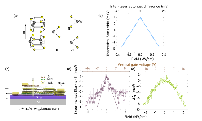
Due to the reflection symmetry in a monolayer WS2 (Figure 2a), in presence of an out-of-plane electric field, the resulting spatial symmetry of the wave function along the c-axis forces the first order perturbation term of the energy eigenvalue to be zero. This causes a zero linear Stark shift in monolayer, and the second order perturbation provides a quadratic QCSE, as verified experimentally 14, 15, 16, 17. However, the reflection symmetry is broken in a bilayer case (Figure 2a) and the resulting asymmetry in the layer distribution of the intra-layer exciton is clearly visible in Figure 1a-b. This in turn results in a nonzero first order perturbation term, and thus a linear QCSE. The electric field dependent linear shift in the intra-layer 1s exciton position as obtained from the solution of the BS equation (see Supporting Information 1 for calculation details) is shown in Figure 2b. We do not consider any additional screening of the electric field inside the bilayer.
To demonstrate the linear QCSE experimentally, and to segregate the electric field effect from the doping effect, we prepare a FLG/hBN/2L-WS2/hBN/FLG (sample S2) stack as schematically shown in Figure 2c (see Methods for sample preparation). The FLG layers act as transparent gate electrodes in the back reflection geometry. The thickness of the top and the bottom hBN layers is 20 nm each. The high quality of the hBN layers allows us to apply high electric field without appreciable gate leakage (see Supporting Information 4). In the field-configuration (denoted as S2-F), a voltage () is applied at the top gate electrode keeping the bottom gate grounded. The electrode directly contacting the bilayer WS2 is kept in open circuit mode, avoiding carrier injection and thus the WS2 is electrically floating. This allows us to study the electric field effect without any confounding electrostatic doping introduced by . In this mode of operation, the lack of gate-induced or photo-induced doping 14 in our sample is evidenced by the absence of any signature of trion in the entire range. The top FLG layer partially covers the device and the sample is illuminated in the FLG-covered portion (Figure 2c). and for the stack are provided in Supporting Information 5 at different electric fields, measured at 4.2 K. The extracted peak shift () with respect to zero field is plotted in Figure 2d as a function of (top axis) and the vertical electric field (bottom axis). The electric field inside the bilayer WS2 is estimated as:
| (2) |
where is the thickness of the bilayer WS2 (hBN), () and () 43 are the static out-of-plane dielectric constants of WS2 and hBN, respectively. We find that varies linearly with - a direct evidence of linear QCSE in bilayer. The average slope of the lines fitting the Stark shift in Figure 2d suggests an out of plane static dipole moment value of meV/MVcm-1. The predicted electric field required to provide the same shift as in the experiment is less in the calculation, which indicates a strong screening 44 in the bilayer WS2, particularly in the presence of optical excitation.
At higher , the experimental Stark shift deviates from linearity as the rate of shift reduces, pointing to strong excitonic effects45 in the QCSE. The exciton binding energy () reduces at higher electric field, which results in a blue shift in the position, partially compensating the QCSE induced red shift. In Figure 2e, we plot the difference between the shift predicted from the fitted line and the experimental values (from Figure 2d), which is an estimate of with an increase in . The reduction in is attributed to two many-body effects. First, an electric field in the out of plane direction forces the electron and hole to move away from each other 46, 47, reducing the spatial overlap of the redistributed wave functions. The second effect arises due to field induced orientation of the excitons in the out of plane direction. The resulting proximity of the particles with similar polarity enhances exciton-exciton repulsion, causing an excitonic blue shift 48, 49.
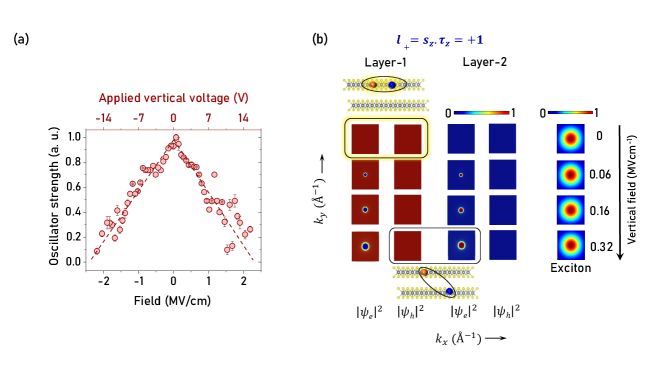
Figure 3a shows that the extracted oscillator strength () of sharply reduces with an increase in , which is promising for atomically thin tunable electro-optic devices. Such a reduction in with increasing is in contrast with monolayer samples, where the photoluminescence intensity is usually a weak function of the vertical field. Since the reduction in binding energy discussed above is quite small compared with , the exciton remains vertically confined in the bilayer 46, 47 and thus dissociation of the exciton under the applied field is an unlikely possibility. As we do not observe any trion peak at higher , in congruence with the floating WS2 channel, transfer of oscillator strength from neutral exciton to trion is also not plausible. We attribute this reduction of to a field driven conversion of intra-layer exciton to inter-layer exciton. The simple Hamiltonian described in Supporting Information 1 is again useful to get a qualitative understanding of the underlying physics. At the left and the middle panels of Figure 3b, we plot, in the two-dimensional space centered around , the fractional contribution of the individual layers to the electron and the hole constituting the exciton at for different vertical fields. The -space distribution of the exciton in the right most panel suggests that the maximum contribution of the 1s exciton is from the states close to . At , the bright exciton arises from electron and hole both lying at the same layer (intra-layer exciton at layer 1 in the top row of Figure 3b). However, with an increase in , the contributing electron concentration around is pushed to the layer 2, while the hole distribution is maintained at layer 1 (bottom three rows). Since there is a large weight of the electronic states close to in the formation of the exciton, this gives rise to an increasing inter-layer character of the exciton. This, in turn, reduces the oscillator strength with an increase in the vertical electric field.
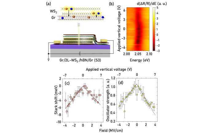
The intra-layer exciton in bilayer WS2 has fast non-radiative scattering channels to lower lying inter-layer exciton at the point 12 and to the indirect band edge states. The relaxation channel can be further aided if the bilayer WS2 is stacked on a few layer graphene, due to ultra-fast inter-layer carrier transfer processes 50, 51, 52, 53, 54 (top panel of Figure 4a). This limits the possibility of re-radiation making the bilayer WS2/graphene stack an excellent atomically thin tunable absorber when excited at the exciton resonance. The ultra-fast charge transfer from WS2 to graphene also results in a strong de-doping of the WS2 layer. This is investigated in a stack of FLG/2L-WS2/hBN/FLG (sample S3), as schematically illustrated in the bottom panel of Figure 4a. The temperature dependent and the corresponding oscillator strength at different temperatures are shown in Supporting Information 6. Figure 4b depicts the in a color plot at different vertical electric fields. The extracted excitonic red shift and the reduction in the oscillator strength are shown separately in Figures 4c-d. While the linearity in the Stark shift is maintained in this structure as well, we observe about -fold reduction in the slope ( meV/MVcm-1) compared with device S2-F, requiring a higher electric field to obtain a similar Stark shift. This can be correlated with the additional screening in the bilayer WS2 due to the proximity of the graphene layer.
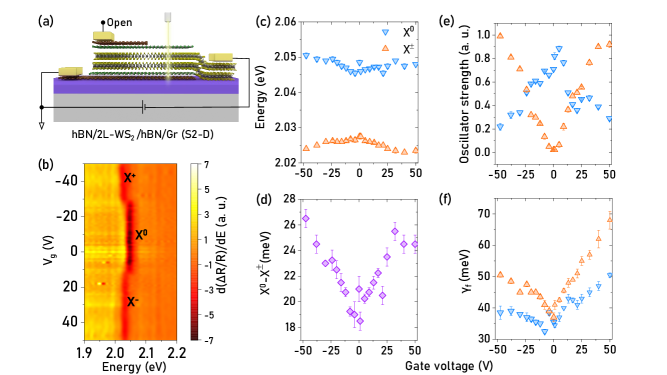
We now investigate the role of electrostatic doping induced by the gate in tuning the intra-layer exciton. For this purpose, we again use sample S2, however, now in a doping configuration (denoted as S2-D). In this mode of operation, the top gate electrode is electrically open circuited, and the metal pad directly contacting the WS2 is electrically grounded. The bottom FLG layer is used as the gate electrode, and a voltage is applied with respect to the grounded electrode, as shown in Figure 5a. The metal contact can efficiently inject both electrons and holes into the bilayer WS2, depending on the polarity of the gate voltage (). Figure 5b shows a two-dimensional color plot of the first derivative of the differential reflectance as a function of (individual spectra are presented in Supporting Information 7). At low , the optical response is dominated by , while at higher positive (negative) , () dominates the response, red shifting the resonance energy.
The small blue shift ( meV) of the exciton with an increase in (Figure 5c) can be attributed to a combined effect of (a) renormalization of the excitonic gap due to the increased doping 55, 56, (b) reduction in exciton binding energy due to separation of electron-hole wave function along the c-axis by the gate field 46, 47, and (c) reduction in the exciton binding energy due to enhanced exciton-exciton repulsion due to oriented exciton dipoles 48, 49. On the other hand, the trion position red shifts with an increase in , leading to an increased separation between the exciton and trion resonance energies (Figure 5d). Similar observations are reported in monolayer as well 57, 58, which is usually attributed to the enhancement in the energy required to move the additional electron (for ) or hole (for ) to respective bands due to doping induced Pauli blocking 59, 52.
The extracted oscillator strength of and in Figure 5e shows a doping dependent transfer of oscillator strength from one excitonic species to another. At low , when the bilayer Fermi level is deep inside the band gap, formation is favoured. Efficient carrier injection in bilayer allows us to sweep the Fermi level almost the entire bandgap, providing strong n-type (p-type) doping at positive (negative) , which favours the formation of (), suppressing the formation of . Such a near complete modulation of oscillator strength of different excitons is promising for electrically tunable ultra-thin optoelectronic components.
We observe a sharp increase in the extracted oscillator strength for both and with an increase in (Figure 5f). For , this is attributed to an enhanced Coulomb scattering in the presence of large electron or hole density, and neutral exciton to trion conversion. The charged nature of the trion species makes the Coulomb scattering stronger resulting in a larger broadening. Similar enhancement in broadening has been observed previously in III-V quantum wells under vertical electric field 46, and has been attributed to increased rate of dissociation of exciton in presence of the electric field. However, in the present case, both the exciton and trion binding energy are significantly larger than their III-V quantum well counterpart. In addition, a stronger quantum confinement in the out of plane direction forces the change in the binding energy to be relatively small, as discussed previously. It thus appears that dissociation induced increase in broadening may play a negligible role in our experiment, particularly for the neutral exciton.
In summary, We propose bilayer WS2 as an atomically thin, tunable electro-absorption layer when excited at the excitonic resonance. The spectral feature as well as the oscillator strength of the excitonic response is highly tunable by an external gate voltage through both electrostatic doping and quantum confined Stark effect. Contrary to the monolayer case, the quantum confined Stark effect in bilayer shows a linear variation with electric field owing to reflection symmetry breaking, coupled with a large modulation in the oscillator strength due to a partial inter-conversion between intra-layer and inter-layer exciton. The electrically tunable nature of the excitonic response has interesting prospects for ultra-thin, light and compact, fast, reconfigurable optoelectronic applications like modulators, pulse shapers, photodetectors, digital mirrors and phased arrays, tuning opacity of surfaces, and possible elements for optical and quantum information processing.
IIScECE] Department of Electrical Communication Engineering, Indian Institute of Science, Bangalore 560012, India IIScECE] Department of Electrical Communication Engineering, Indian Institute of Science, Bangalore 560012, India IIScECE] Department of Electrical Communication Engineering, Indian Institute of Science, Bangalore 560012, India IIScECE] Department of Electrical Communication Engineering, Indian Institute of Science, Bangalore 560012, India IIScECE] Department of Electrical Communication Engineering, Indian Institute of Science, Bangalore 560012, India NBI] Center for Quantum Devices, Niels Bohr Institute, University of Copenhagen, Denmark NIMS1] Research Center for Functional Materials, National Institute for Materials Science, 1-1 Namiki, Tsukuba 305-044, Japan NIMS2] International Center for Materials Nanoarchitectonics, National Institute for Materials Science, 1-1 Namiki, Tsukuba, 305-044 Japan IIScECE] Department of Electrical Communication Engineering, Indian Institute of Science, Bangalore 560012, India
Keywords: 2D materials, transition metal dichalcogenide, excitonic reflection, absorption, spectral tuning, electric field, oscillator strength.
The ultra-fast radiative recombination rate 1, 2, 3 of the strongly bound excitons 4, 5, 6 in monolayer transition metal dichalcogenides (TMDCs) leads to efficient photoemission 7, 8. The fast re-radiation of the absorbed photon by the exciton without ample opportunity to suffer from non-radiative processes results in near perfect excitonic reflectance 9, 10, 11. On the other hand, in a bilayer TMDC, a lower indirect energy bandgap appears while the direct energy gap at the point of the Brillouin zone is maintained. This causes the momentum-direct excitons in bilayer to encounter strong non-radiative processes 12, and thus a bilayer TMDC is weakly luminescent 13, while still exhibiting strong excitonic absorption.
To be able to tune the excitonic absorbtion in a dynamic manner is crucial to multiple applications such as programmable optical modulators, tunable photodetectors, optical computing and imaging, laser pulse shaping, and ultra-light optomechanical mirrors. A bilayer distinguishes itself from the monolayers in a number of ways in terms of tunability of the exciton oscillator strength and its spectral control. First, the reflection symmetry along the c-axis is present in a monolayer TMDC, but is broken in a bilayer. Thus, in presence of a vertical electric field, one expects that a bilayer would show linear Stark shift, in contrast to a quadratic one 14, 15, 16, 17 in monolayer. In spite of theoretical predictions of linear quantum confined Stark effect (QCSE) in bilayer TMDC 18, 19, 20, 21, 22, 23, 24, 25, there has not been any experimental demonstration of the same to date for the direct intra-layer exciton. Second, the presence of two layers in a bilayer, which are rotated at with respect to each other, offers an additional layer degree of freedom 12. With a vertical electric field, there is a possibility to convert the intra-layer exciton at zero field to an inter-layer exciton, resulting in a strong tunability of the oscillator strength. Third, it is easier to inject carriers in a bilayer from a metal contact due to reduced bandgap, increased valley degeneracy and enhanced orbital coupling to metal 26. This allows fast and efficient modulation of the excitonic oscillator strength by inter-conversion between a neutral exciton and a charge exciton (trion) through electrostatic doping 27, 28, 29.
In this work we use two different device structures to segregate the effects of electric field induced QCSE and electrostatically induced doping on both the strength and the spectral tunability of the excitonic response in a bilayer WS2. We use a few-layer graphene (FLG)/hBN/2L-WS2/hBN/FLG stack keeping the bilayer WS2 electrically floating to report linear QCSE of the direct intra-layer exciton. The corresponding excitonic oscillator strength is shown to exhibit a large tunability due to an electric field driven partial inter-conversion between intra-layer and inter-layer exciton. We further demonstrate that placing a graphene layer right under the bilayer WS2 is promising for an atomically thin, gate tunable electro-absorption layer. To demonstrate the electrostatically induced doping effect, we use a similar stack, but with the bilayer WS2 connected to a grounded metal contact. The efficient carrier injection from the contact leads to effective oscillator strength transfer from neutral exciton to positive or negatively charged trions depending on the polarity of the gate voltage.
In the 2H form of bilayer WS2, the individual layers are rotated by 180∘ with respect to each other, making the unit cell inversion symmetric. This requires an additional layer degree of freedom () to describe excitons in bilayer for a given spin () and valley (). To describe the lowest energy excitonic states in a bilayer, we use a simple quasiparticle Hamiltonian using tungsten orbitals as the basis functions 30, 12 and solve the Bethe-Salpeter (BS) equation31, 12, as described in Supporting Information 1. As an example, in Figure 1a, we schematically illustrate the lowest energy conduction and valence bands for one of the degenerate cases () along with the layer distribution of the wave functions close to point. The energy dispersion of lowest energy excitonic states with center of mass momentum () is schematically depicted in Figure 1b. The calculated -space distribution of the excitonic state with is depicted in Figure 1c. Depending on the layer distribution of the single particle wave functions, we have both intra-layer [] and inter-layer [] 1s excitons, with the latter being the lowest energy one for bilayer WS2. The layer index of the intra-layer exciton is coupled with spin and valley such that =.= 12, which results in two degenerate configurations for each at zero external field. While radiative recombination is allowed for both these types of excitons by standard selection rules, the intra-layer exciton exhibits more than an order of magnitude higher radiative decay rate compared with the inter-layer exciton 12, and hence the optical response in bilayer discussed here is dominated by the intra-layer exciton 32. The inter-layer exciton noted above is momentum-direct with 12, 33, 34, 35, 36, which is distinct from the indirect inter-layer exciton 37, 38. Due to the difference in spin splitting of the bright and the dark states in Mo and W-based TMDCs, the inter-layer exciton is energetically above the intra-layer exciton in MoTe2 33, MoSe2 34, and MoS2 35, 36, 39, while it is below the intra-layer exciton in WS2 12.
To extract the spectral feature of the intra-layer exciton in isolated bilayer WS2 transferred on 285 nm SiO2/Si substrate (sample S1 as schematically shown in Figure 1d, see Supporting Information 2 for Raman Characterization), we perform differential reflectance measurement (see Methods for measurement details). Figure 1e shows the temperature dependent differential reflectance () in the range of to K. Throughout the text, denotes the reflected intensity from full stack and denotes the same from the stack without the bilayer WS2. For notational simplicity, we denote experimentally observed neutral exciton and charged trion peaks as and , respectively. The optical response and the line shape are modified by the interference between WS2 and substrate reflection, and the excitonic response of the bilayer is deconvoluted from the overall response. To reproduce the reflectance spectra obtained from the experiment, the exciton contribution to the dielectric response is represented as Lorentzian oscillator 40, 41, 42:
| (1) |
where the is the background response, and are the oscillator strength and the position of the oscillator respectively with a broadening parameter . and are then calculated using transfer matrix method (see Supporting Information 3 for more details). The color plot of in Figure 1f shows a conspicuous spectral red shift of the neutral exciton with an increase in temperature, which results from a corresponding reduction in the bandgap. The corresponding temperature tunability of the exciton oscillator strength is shown in Figure 1g.
Due to the reflection symmetry in a monolayer WS2 (Figure 2a), in presence of an out-of-plane electric field, the resulting spatial symmetry of the wave function along the c-axis forces the first order perturbation term of the energy eigenvalue to be zero. This causes a zero linear Stark shift in monolayer, and the second order perturbation provides a quadratic QCSE, as verified experimentally 14, 15, 16, 17. However, the reflection symmetry is broken in a bilayer case (Figure 2a) and the resulting asymmetry in the layer distribution of the intra-layer exciton is clearly visible in Figure 1a-b. This in turn results in a nonzero first order perturbation term, and thus a linear QCSE. The electric field dependent linear shift in the intra-layer 1s exciton position as obtained from the solution of the BS equation (see Supporting Information 1 for calculation details) is shown in Figure 2b. We do not consider any additional screening of the electric field inside the bilayer.
To demonstrate the linear QCSE experimentally, and to segregate the electric field effect from the doping effect, we prepare a FLG/hBN/2L-WS2/hBN/FLG (sample S2) stack as schematically shown in Figure 2c (see Methods for sample preparation). The FLG layers act as transparent gate electrodes in the back reflection geometry. The thickness of the top and the bottom hBN layers is 20 nm each. The high quality of the hBN layers allows us to apply high electric field without appreciable gate leakage (see Supporting Information 4). In the field-configuration (denoted as S2-F), a voltage () is applied at the top gate electrode keeping the bottom gate grounded. The electrode directly contacting the bilayer WS2 is kept in open circuit mode, avoiding carrier injection and thus the WS2 is electrically floating. This allows us to study the electric field effect without any confounding electrostatic doping introduced by . In this mode of operation, the lack of gate-induced or photo-induced doping 14 in our sample is evidenced by the absence of any signature of trion in the entire range. The top FLG layer partially covers the device and the sample is illuminated in the FLG-covered portion (Figure 2c). and for the stack are provided in Supporting Information 5 at different electric fields, measured at 4.2 K. The extracted peak shift () with respect to zero field is plotted in Figure 2d as a function of (top axis) and the vertical electric field (bottom axis). The electric field inside the bilayer WS2 is estimated as:
| (2) |
where is the thickness of the bilayer WS2 (hBN), () and () 43 are the static out-of-plane dielectric constants of WS2 and hBN, respectively. We find that varies linearly with - a direct evidence of linear QCSE in bilayer. The average slope of the lines fitting the Stark shift in Figure 2d suggests an out of plane static dipole moment value of meV/MVcm-1. The predicted electric field required to provide the same shift as in the experiment is less in the calculation, which indicates a strong screening 44 in the bilayer WS2, particularly in the presence of optical excitation.
At higher , the experimental Stark shift deviates from linearity as the rate of shift reduces, pointing to strong excitonic effects45 in the QCSE. The exciton binding energy () reduces at higher electric field, which results in a blue shift in the position, partially compensating the QCSE induced red shift. In Figure 2e, we plot the difference between the shift predicted from the fitted line and the experimental values (from Figure 2d), which is an estimate of with an increase in . The reduction in is attributed to two many-body effects. First, an electric field in the out of plane direction forces the electron and hole to move away from each other 46, 47, reducing the spatial overlap of the redistributed wave functions. The second effect arises due to field induced orientation of the excitons in the out of plane direction. The resulting proximity of the particles with similar polarity enhances exciton-exciton repulsion, causing an excitonic blue shift 48, 49.
Figure 3a shows that the extracted oscillator strength () of sharply reduces with an increase in , which is promising for atomically thin tunable electro-optic devices. Such a reduction in with increasing is in contrast with monolayer samples, where the photoluminescence intensity is usually a weak function of the vertical field. Since the reduction in binding energy discussed above is quite small compared with , the exciton remains vertically confined in the bilayer 46, 47 and thus dissociation of the exciton under the applied field is an unlikely possibility. As we do not observe any trion peak at higher , in congruence with the floating WS2 channel, transfer of oscillator strength from neutral exciton to trion is also not plausible. We attribute this reduction of to a field driven conversion of intra-layer exciton to inter-layer exciton. The simple Hamiltonian described in Supporting Information 1 is again useful to get a qualitative understanding of the underlying physics. At the left and the middle panels of Figure 3b, we plot, in the two-dimensional space centered around , the fractional contribution of the individual layers to the electron and the hole constituting the exciton at for different vertical fields. The -space distribution of the exciton in the right most panel suggests that the maximum contribution of the 1s exciton is from the states close to . At , the bright exciton arises from electron and hole both lying at the same layer (intra-layer exciton at layer 1 in the top row of Figure 3b). However, with an increase in , the contributing electron concentration around is pushed to the layer 2, while the hole distribution is maintained at layer 1 (bottom three rows). Since there is a large weight of the electronic states close to in the formation of the exciton, this gives rise to an increasing inter-layer character of the exciton. This, in turn, reduces the oscillator strength with an increase in the vertical electric field.
The intra-layer exciton in bilayer WS2 has fast non-radiative scattering channels to lower lying inter-layer exciton at the point 12 and to the indirect band edge states. The relaxation channel can be further aided if the bilayer WS2 is stacked on a few layer graphene, due to ultra-fast inter-layer carrier transfer processes 50, 51, 52, 53, 54 (top panel of Figure 4a). This limits the possibility of re-radiation making the bilayer WS2/graphene stack an excellent atomically thin tunable absorber when excited at the exciton resonance. The ultra-fast charge transfer from WS2 to graphene also results in a strong de-doping of the WS2 layer. This is investigated in a stack of FLG/2L-WS2/hBN/FLG (sample S3), as schematically illustrated in the bottom panel of Figure 4a. The temperature dependent and the corresponding oscillator strength at different temperatures are shown in Supporting Information 6. Figure 4b depicts the in a color plot at different vertical electric fields. The extracted excitonic red shift and the reduction in the oscillator strength are shown separately in Figures 4c-d. While the linearity in the Stark shift is maintained in this structure as well, we observe about -fold reduction in the slope ( meV/MVcm-1) compared with device S2-F, requiring a higher electric field to obtain a similar Stark shift. This can be correlated with the additional screening in the bilayer WS2 due to the proximity of the graphene layer.
We now investigate the role of electrostatic doping induced by the gate in tuning the intra-layer exciton. For this purpose, we again use sample S2, however, now in a doping configuration (denoted as S2-D). In this mode of operation, the top gate electrode is electrically open circuited, and the metal pad directly contacting the WS2 is electrically grounded. The bottom FLG layer is used as the gate electrode, and a voltage is applied with respect to the grounded electrode, as shown in Figure 5a. The metal contact can efficiently inject both electrons and holes into the bilayer WS2, depending on the polarity of the gate voltage (). Figure 5b shows a two-dimensional color plot of the first derivative of the differential reflectance as a function of (individual spectra are presented in Supporting Information 7). At low , the optical response is dominated by , while at higher positive (negative) , () dominates the response, red shifting the resonance energy.
The small blue shift ( meV) of the exciton with an increase in (Figure 5c) can be attributed to a combined effect of (a) renormalization of the excitonic gap due to the increased doping 55, 56, (b) reduction in exciton binding energy due to separation of electron-hole wave function along the c-axis by the gate field 46, 47, and (c) reduction in the exciton binding energy due to enhanced exciton-exciton repulsion due to oriented exciton dipoles 48, 49. On the other hand, the trion position red shifts with an increase in , leading to an increased separation between the exciton and trion resonance energies (Figure 5d). Similar observations are reported in monolayer as well 57, 58, which is usually attributed to the enhancement in the energy required to move the additional electron (for ) or hole (for ) to respective bands due to doping induced Pauli blocking 59, 52.
The extracted oscillator strength of and in Figure 5e shows a doping dependent transfer of oscillator strength from one excitonic species to another. At low , when the bilayer Fermi level is deep inside the band gap, formation is favoured. Efficient carrier injection in bilayer allows us to sweep the Fermi level almost the entire bandgap, providing strong n-type (p-type) doping at positive (negative) , which favours the formation of (), suppressing the formation of . Such a near complete modulation of oscillator strength of different excitons is promising for electrically tunable ultra-thin optoelectronic components.
We observe a sharp increase in the extracted oscillator strength for both and with an increase in (Figure 5f). For , this is attributed to an enhanced Coulomb scattering in the presence of large electron or hole density, and neutral exciton to trion conversion. The charged nature of the trion species makes the Coulomb scattering stronger resulting in a larger broadening. Similar enhancement in broadening has been observed previously in III-V quantum wells under vertical electric field 46, and has been attributed to increased rate of dissociation of exciton in presence of the electric field. However, in the present case, both the exciton and trion binding energy are significantly larger than their III-V quantum well counterpart. In addition, a stronger quantum confinement in the out of plane direction forces the change in the binding energy to be relatively small, as discussed previously. It thus appears that dissociation induced increase in broadening may play a negligible role in our experiment, particularly for the neutral exciton.
In summary, We propose bilayer WS2 as an atomically thin, tunable electro-absorption layer when excited at the excitonic resonance. The spectral feature as well as the oscillator strength of the excitonic response is highly tunable by an external gate voltage through both electrostatic doping and quantum confined Stark effect. Contrary to the monolayer case, the quantum confined Stark effect in bilayer shows a linear variation with electric field owing to reflection symmetry breaking, coupled with a large modulation in the oscillator strength due to a partial inter-conversion between intra-layer and inter-layer exciton. The electrically tunable nature of the excitonic response has interesting prospects for ultra-thin, light and compact, fast, reconfigurable optoelectronic applications like modulators, pulse shapers, photodetectors, digital mirrors and phased arrays, tuning opacity of surfaces, and possible elements for optical and quantum information processing.
Methods
Device fabrication: The heterojunctions are prepared using dry transfer of individual exfoliated layers to a Si substrate coated with 285 nm SiO2 layer. The transfer of each layer is performed one at a time under a microscope with controlled translational and rotational stages for precise alignment. After transfer of each layer, the sample is heated on a hot plate at C for 2 minutes for improved adhesion between layers. Optical images of samples S2 and S3 are shown in Supporting Information 8 after all the layers are transferred. Standard nanofabrication techniques are used to define the metal electrodes contacting the graphene layers. The substrate with the transferred layers is spin coated with PMMA 950C3 and baked on a hot plate at C for 2 minutes. This is followed by electron beam lithography with an acceleration voltage of 20 KV, an electron beam current of 210 pA, and an electron beam dose of 220 Ccm-2. Patterns are developed using MIBK:IPA solution in the ratio 1:3. Later samples are washed in IPA and dried in N2 blow. Electrodes are made with 10 nm Ni /50 nm Au films deposited by DC magnetron sputtering at mBar. Metal lift-off is done by dipping the substrate in acetone for 20 minutes, followed by washing in IPA and N2 drying.
Reflectance measurement: For temperature dependent micro-reflectance measurements, the samples are placed in a closed cycle He cryostat with an optical window placed above the sample. The samples are illuminated with a broadband white LED source and response is collected through a objective with a numerical aperture of 0.5 and analyzed using a spectrometer with a grating of 1800 lines/mm. The differential reflectance is then calculated via normalizing the signal obtained from stack with () and without bilayer WS2 () layer as follows: . To match the experimental data, apart from the exciton, we consider oscillators separated by meV in the spectral range below the exciton while the higher energy side is fitted with oscillators placed at , , , , and energy positions 4, 5.
Supporting Information
S1. Stark shift calculation of the excitons in bilayer TMD, S2. Raman characterization of bilayer WS2, S3. Calculation of reflectance with transfer matrix method, S4. Gate leakage current for sample S2, S5. Field dependent differential reflectance for the device configuration S2-F, S6. Temperature dependent reflectance spectra for sample S3, S7. Gate dependent reflectance spectra for device configuration S2-D, S8. Optical images of the stacks.
Acknowledgements
K. M. thanks Varun Raghunathan for useful discussions. K. M. acknowledges the support a grant from Indian Space Research Organization (ISRO), a grant from MHRD under STARS, grants under Ramanujan Fellowship and Nano Mission from the Department of Science and Technology (DST), Government of India, and support from MHRD, MeitY and DST Nano Mission through NNetRA. K.W. and T.T. acknowledge support from the Elemental Strategy Initiative conducted by the MEXT, Japan, Grant Number JPMXP0112101001, JSPS KAKENHI Grant Numbers JP20H00354 and the CREST(JPMJCR15F3), JST.
Competing Interests
The Authors declare no Competing Financial or Non-Financial Interests.
References
- Robert et al. 2016 Robert, C.; Lagarde, D.; Cadiz, F.; Wang, G.; Lassagne, B.; Amand, T.; Balocchi, A.; Renucci, P.; Tongay, S.; Urbaszek, B., et al. Exciton radiative lifetime in transition metal dichalcogenide monolayers. Physical Review B 2016, 93, 205423
- Palummo et al. 2015 Palummo, M.; Bernardi, M.; Grossman, J. C. Exciton radiative lifetimes in two-dimensional transition metal dichalcogenides. Nano letters 2015, 15, 2794–2800
- Gupta and Majumdar 2019 Gupta, G.; Majumdar, K. Fundamental exciton linewidth broadening in monolayer transition metal dichalcogenides. Physical Review B 2019, 99, 085412
- He et al. 2014 He, K.; Kumar, N.; Zhao, L.; Wang, Z.; Mak, K. F.; Zhao, H.; Shan, J. Tightly bound excitons in monolayer WSe 2. Physical review letters 2014, 113, 026803
- Chernikov et al. 2014 Chernikov, A.; Berkelbach, T. C.; Hill, H. M.; Rigosi, A.; Li, Y.; Aslan, O. B.; Reichman, D. R.; Hybertsen, M. S.; Heinz, T. F. Exciton binding energy and nonhydrogenic Rydberg series in monolayer WS 2. Physical review letters 2014, 113, 076802
- Gupta et al. 2017 Gupta, G.; Kallatt, S.; Majumdar, K. Direct observation of giant binding energy modulation of exciton complexes in monolayer MoS e 2. Physical Review B 2017, 96, 081403
- Splendiani et al. 2010 Splendiani, A.; Sun, L.; Zhang, Y.; Li, T.; Kim, J.; Chim, C.-Y.; Galli, G.; Wang, F. Emerging photoluminescence in monolayer MoS2. Nano letters 2010, 10, 1271–1275
- Paur et al. 2019 Paur, M.; Molina-Mendoza, A. J.; Bratschitsch, R.; Watanabe, K.; Taniguchi, T.; Mueller, T. Electroluminescence from multi-particle exciton complexes in transition metal dichalcogenide semiconductors. Nature communications 2019, 10, 1–7
- Scuri et al. 2018 Scuri, G.; Zhou, Y.; High, A. A.; Wild, D. S.; Shu, C.; De Greve, K.; Jauregui, L. A.; Taniguchi, T.; Watanabe, K.; Kim, P., et al. Large excitonic reflectivity of monolayer MoSe 2 encapsulated in hexagonal boron nitride. Physical review letters 2018, 120, 037402
- Back et al. 2018 Back, P.; Zeytinoglu, S.; Ijaz, A.; Kroner, M.; Imamoğlu, A. Realization of an electrically tunable narrow-bandwidth atomically thin mirror using monolayer MoSe 2. Physical review letters 2018, 120, 037401
- Zhou et al. 2020 Zhou, Y.; Scuri, G.; Sung, J.; Gelly, R. J.; Wild, D. S.; De Greve, K.; Joe, A. Y.; Taniguchi, T.; Watanabe, K.; Kim, P., et al. Controlling excitons in an atomically thin membrane with a mirror. Physical Review Letters 2020, 124, 027401
- Das et al. 2019 Das, S.; Gupta, G.; Majumdar, K. Layer degree of freedom for excitons in transition metal dichalcogenides. Physical Review B 2019, 99, 165411
- Mak et al. 2010 Mak, K. F.; Lee, C.; Hone, J.; Shan, J.; Heinz, T. F. Atomically thin MoS 2: a new direct-gap semiconductor. Physical review letters 2010, 105, 136805
- Verzhbitskiy et al. 2019 Verzhbitskiy, I.; Vella, D.; Watanabe, K.; Taniguchi, T.; Eda, G. Suppressed Out-of-Plane Polarizability of Free Excitons in Monolayer WSe2. ACS nano 2019, 13, 3218–3224
- Roch et al. 2018 Roch, J. G.; Leisgang, N.; Froehlicher, G.; Makk, P.; Watanabe, K.; Taniguchi, T.; Schonenberger, C.; Warburton, R. J. Quantum-confined stark effect in a MoS2 monolayer van der Waals heterostructure. Nano letters 2018, 18, 1070–1074
- Massicotte et al. 2018 Massicotte, M.; Vialla, F.; Schmidt, P.; Lundeberg, M. B.; Latini, S.; Haastrup, S.; Danovich, M.; Davydovskaya, D.; Watanabe, K.; Taniguchi, T., et al. Dissociation of two-dimensional excitons in monolayer WSe 2. Nature communications 2018, 9, 1–7
- Chakraborty et al. 2019 Chakraborty, C.; Mukherjee, A.; Qiu, L.; Vamivakas, A. N. Electrically tunable valley polarization and valley coherence in monolayer WSe 2 embedded in a van der Waals heterostructure. Optical Materials Express 2019, 9, 1479–1487
- Liu et al. 2012 Liu, Q.; Li, L.; Li, Y.; Gao, Z.; Chen, Z.; Lu, J. Tuning electronic structure of bilayer MoS2 by vertical electric field: a first-principles investigation. The Journal of Physical Chemistry C 2012, 116, 21556–21562
- Lu and Yang 2017 Lu, X.; Yang, L. Stark effect of doped two-dimensional transition metal dichalcogenides. Applied Physics Letters 2017, 111, 193104
- Nguyen et al. 2016 Nguyen, C. V.; Hieu, N. N.; Ilyasov, V. V. Band gap modulation of bilayer MoS 2 under strain engineering and electric field: A density functional theory. Journal of Electronic Materials 2016, 45, 4038–4043
- Ramasubramaniam et al. 2011 Ramasubramaniam, A.; Naveh, D.; Towe, E. Tunable band gaps in bilayer transition-metal dichalcogenides. Physical Review B 2011, 84, 205325
- Yang and Ni 2010 Yang, Z.; Ni, J. Modulation of electronic properties of hexagonal boron nitride bilayers by an electric field: a first principles study. Journal of Applied Physics 2010, 107, 104301
- Zibouche et al. 2014 Zibouche, N.; Philipsen, P.; Kuc, A.; Heine, T. Transition-metal dichalcogenide bilayers: Switching materials for spintronic and valleytronic applications. Physical Review B 2014, 90, 125440
- Shanavas and Satpathy 2015 Shanavas, K. V.; Satpathy, S. Effective tight-binding model for M X 2 under electric and magnetic fields. Physical Review B 2015, 91, 235145
- Zhang et al. 2014 Zhang, Z.; Si, M.; Wang, Y.; Gao, X.; Sung, D.; Hong, S.; He, J. Indirect-direct band gap transition through electric tuning in bilayer MoS2. The Journal of chemical physics 2014, 140, 174707
- Kim et al. 2012 Kim, S.; Konar, A.; Hwang, W.-S.; Lee, J. H.; Lee, J.; Yang, J.; Jung, C.; Kim, H.; Yoo, J.-B.; Choi, J.-Y., et al. High-mobility and low-power thin-film transistors based on multilayer MoS 2 crystals. Nature communications 2012, 3, 1–7
- Pei et al. 2015 Pei, J.; Yang, J.; Xu, R.; Zeng, Y.-H.; Myint, Y. W.; Zhang, S.; Zheng, J.-C.; Qin, Q.; Wang, X.; Jiang, W., et al. Exciton and trion dynamics in bilayer MoS2. Small 2015, 11, 6384–6390
- Kümmell et al. 2015 Kümmell, T.; Quitsch, W.; Matthis, S.; Litwin, T.; Bacher, G. Gate control of carrier distribution in k-space in MoS 2 monolayer and bilayer crystals. Physical Review B 2015, 91, 125305
- Wu et al. 2013 Wu, S.; Ross, J. S.; Liu, G.-B.; Aivazian, G.; Jones, A.; Fei, Z.; Zhu, W.; Xiao, D.; Yao, W.; Cobden, D., et al. Electrical tuning of valley magnetic moment through symmetry control in bilayer MoS 2. Nature Physics 2013, 9, 149–153
- Gong et al. 2013 Gong, Z.; Liu, G.-B.; Yu, H.; Xiao, D.; Cui, X.; Xu, X.; Yao, W. Magnetoelectric effects and valley-controlled spin quantum gates in transition metal dichalcogenide bilayers. Nature communications 2013, 4, 1–6
- Wu et al. 2015 Wu, F.; Qu, F.; Macdonald, A. H. Exciton band structure of monolayer MoS 2. Physical Review B 2015, 91, 075310
- Schuller et al. 2013 Schuller, J. A.; Karaveli, S.; Schiros, T.; He, K.; Yang, S.; Kymissis, I.; Shan, J.; Zia, R. Orientation of luminescent excitons in layered nanomaterials. Nature nanotechnology 2013, 8, 271–276
- Arora et al. 2017 Arora, A.; Drüppel, M.; Schmidt, R.; Deilmann, T.; Schneider, R.; Molas, M. R.; Marauhn, P.; de Vasconcellos, S. M.; Potemski, M.; Rohlfing, M., et al. Interlayer excitons in a bulk van der Waals semiconductor. Nature communications 2017, 8, 1–6
- Horng et al. 2018 Horng, J.; Stroucken, T.; Zhang, L.; Paik, E. Y.; Deng, H.; Koch, S. W. Observation of interlayer excitons in MoSe 2 single crystals. Physical Review B 2018, 97, 241404
- Niehues et al. 2019 Niehues, I.; Blob, A.; Stiehm, T.; de Vasconcellos, S. M.; Bratschitsch, R. Interlayer excitons in bilayer MoS 2 under uniaxial tensile strain. Nanoscale 2019, 11, 12788–12792
- Gerber et al. 2019 Gerber, I. C.; Courtade, E.; Shree, S.; Robert, C.; Taniguchi, T.; Watanabe, K.; Balocchi, A.; Renucci, P.; Lagarde, D.; Marie, X., et al. Interlayer excitons in bilayer MoS 2 with strong oscillator strength up to room temperature. Physical Review B 2019, 99, 035443
- Wang et al. 2018 Wang, Z.; Chiu, Y.-H.; Honz, K.; Mak, K. F.; Shan, J. Electrical tuning of interlayer exciton gases in WSe2 bilayers. Nano letters 2018, 18, 137–143
- Scuri et al. 2020 Scuri, G.; Andersen, T. I.; Zhou, Y.; Wild, D. S.; Sung, J.; Gelly, R. J.; Bérubé, D.; Heo, H.; Shao, L.; Joe, A. Y., et al. Electrically tunable valley dynamics in twisted WSe 2/WSe 2 bilayers. Physical Review Letters 2020, 124, 217403
- Leisgang et al. 2020 Leisgang, N.; Shree, S.; Paradisanos, I.; Sponfeldner, L.; Robert, C.; Lagarde, D.; Balocchi, A.; Watanabe, K.; Taniguchi, T.; Marie, X., et al. Giant Stark splitting of an exciton in bilayer MoS2. Nature Nanotechnology 2020, https://doi.org/10.1038/s41565–020–0750–1
- Li et al. 2014 Li, Y.; Chernikov, A.; Zhang, X.; Rigosi, A.; Hill, H. M.; Van Der Zande, A. M.; Chenet, D. A.; Shih, E.-M.; Hone, J.; Heinz, T. F. Measurement of the optical dielectric function of monolayer transition-metal dichalcogenides: MoS2, MoSe2, WS2, and WSe2. Physical Review B 2014, 90, 205422
- Arora et al. 2015 Arora, A.; Koperski, M.; Nogajewski, K.; Marcus, J.; Faugeras, C.; Potemski, M. Excitonic resonances in thin films of WSe 2: from monolayer to bulk material. Nanoscale 2015, 7, 10421–10429
- Yu et al. 2017 Yu, Y.; Yu, Y.; Huang, L.; Peng, H.; Xiong, L.; Cao, L. Giant gating tunability of optical refractive index in transition metal dichalcogenide monolayers. Nano letters 2017, 17, 3613–3618
- Laturia et al. 2018 Laturia, A.; Van de Put, M. L.; Vandenberghe, W. G. Dielectric properties of hexagonal boron nitride and transition metal dichalcogenides: from monolayer to bulk. npj 2D Materials and Applications 2018, 2, 1–7
- Santos and Kaxiras 2013 Santos, E. J.; Kaxiras, E. Electrically driven tuning of the dielectric constant in MoS2 layers. ACS nano 2013, 7, 10741–10746
- Abraham et al. 2020 Abraham, N.; Watanabe, K.; Taniguchi, T.; Majumdar, K. Anomalous Stark Shift of Excitonic Complexes in Monolayer Semiconductor. arXiv preprint arXiv:2011.00221 2020,
- Miller et al. 1984 Miller, D. A.; Chemla, D.; Damen, T.; Gossard, A.; Wiegmann, W.; Wood, T.; Burrus, C. Band-edge electroabsorption in quantum well structures: The quantum-confined Stark effect. Physical Review Letters 1984, 53, 2173
- Polland et al. 1985 Polland, H.-J.; Schultheis, L.; Kuhl, J.; Göbel, E.; Tu, C. Lifetime enhancement of two-dimensional excitons by the quantum-confined Stark effect. Physical review letters 1985, 55, 2610
- Sie et al. 2017 Sie, E. J.; Steinhoff, A.; Gies, C.; Lui, C. H.; Ma, Q.; Rosner, M.; Schonhoff, G.; Jahnke, F.; Wehling, T. O.; Lee, Y.-H., et al. Observation of exciton redshift–blueshift crossover in monolayer WS2. Nano letters 2017, 17, 4210–4216
- Unuchek et al. 2019 Unuchek, D.; Ciarrocchi, A.; Avsar, A.; Sun, Z.; Watanabe, K.; Taniguchi, T.; Kis, A. Valley-polarized exciton currents in a van der Waals heterostructure. Nature nanotechnology 2019, 14, 1104–1109
- Ceballos et al. 2014 Ceballos, F.; Bellus, M. Z.; Chiu, H.-Y.; Zhao, H. Ultrafast charge separation and indirect exciton formation in a MoS2–MoSe2 van der Waals heterostructure. ACS Nano 2014, 8, 12717–12724
- Hong et al. 2014 Hong, X.; Kim, J.; Shi, S.-F.; Zhang, Y.; Jin, C.; Sun, Y.; Tongay, S.; Wu, J.; Zhang, Y.; Wang, F. Ultrafast charge transfer in atomically thin MoS2/WS2 heterostructures. Nature Nanotechnology 2014, 9, 682
- Kallatt et al. 2019 Kallatt, S.; Das, S.; Chatterjee, S.; Majumdar, K. Interlayer charge transport controlled by exciton–trion coherent coupling. npj 2D Materials and Applications 2019, 3, 1–8
- Jauregui et al. 2019 Jauregui, L. A.; Joe, A. Y.; Pistunova, K.; Wild, D. S.; High, A. A.; Zhou, Y.; Scuri, G.; De Greve, K.; Sushko, A.; Yu, C.-H., et al. Electrical control of interlayer exciton dynamics in atomically thin heterostructures. Science 2019, 366, 870–875
- Das et al. 2020 Das, S.; Kallatt, S.; Abraham, N.; Majumdar, K. Gate-tunable trion switch for excitonic device applications. Physical Review B 2020, 101, 081413
- Chernikov et al. 2015 Chernikov, A.; Van Der Zande, A. M.; Hill, H. M.; Rigosi, A. F.; Velauthapillai, A.; Hone, J.; Heinz, T. F. Electrical tuning of exciton binding energies in monolayer WS 2. Physical review letters 2015, 115, 126802
- Yao et al. 2017 Yao, K.; Yan, A.; Kahn, S.; Suslu, A.; Liang, Y.; Barnard, E. S.; Tongay, S.; Zettl, A.; Borys, N. J.; Schuck, P. J. Optically discriminating carrier-induced quasiparticle band gap and exciton energy renormalization in monolayer MoS 2. Physical Review Letters 2017, 119, 087401
- Xu et al. 2014 Xu, X.; Yao, W.; Xiao, D.; Heinz, T. F. Spin and pseudospins in layered transition metal dichalcogenides. Nature Physics 2014, 10, 343–350
- Li et al. 2019 Li, Z.; Wang, T.; Jin, C.; Lu, Z.; Lian, Z.; Meng, Y.; Blei, M.; Gao, S.; Taniguchi, T.; Watanabe, K., et al. Emerging photoluminescence from the dark-exciton phonon replica in monolayer WSe 2. Nature communications 2019, 10, 1–7
- Mak et al. 2013 Mak, K. F.; He, K.; Lee, C.; Lee, G. H.; Hone, J.; Heinz, T. F.; Shan, J. Tightly bound trions in monolayer MoS 2. Nature materials 2013, 12, 207–211
See pages 2-11 of si