Interface enhanced helicity dependent photocurrent in metal/semimetal bilayers
Abstract
One of the hallmarks of light-spin interaction in solids is the appearance of photocurrent that depends on the light helicity. Recent studies have shown that helicity dependent photocurrent (HDP) emerges due to light induced spin current and the inverse spin Hall effect of semimetal thin films. We have studied HDP in metal/semimetal bilayers. Compared to Bi single layer films, we find the HDP is enhanced in metal/Bi bilayers. For the bilayers, the sign of HDP under back illumination reverses from that of front illumination. The back illumination photocurrent is the largest for Ag/Bi bilayers among the bilayers studied. Using a diffusive spin transport model, we show that the HDP sign reversal under back illumination is caused by spin absorption and spin to charge conversion at the interface. Such interfacial effects contribute to the HDP enhancement under front illumination for the bilayers when the Bi layer thickness is small. These results show that the HDP can be used to assess interface states with strong spin orbit coupling.
The exchange of spin angular momentum between electrons plays a fundamental role in modern spintronics as it allows current induced control of magnetismManchon et al. (2019). The concept can be extended to interaction of electron spins with light: the transfer of spin angular momentum from light to electrons allow manipulation of magnetization using ultrashort laser pulses in magnetic thin filmsKimel et al. (2005); Stanciu et al. (2007); Lambert et al. (2014). The interaction of light with electron spin also manifests itself in photocurrents, i.e. currents that flow when light is irradiated to solids. For example, irradiation of circularly polarized light to materials that possess spin-momentum locked bands results in generation of helicity dependent anisotropic photocurrent. The effect, often referred to as the circularly photogalvanic effect (CPGE), has been identified in semiconductor heterostructuresGanichev et al. (2002, 2004), topological surface statesMcIver et al. (2012); Okada et al. (2016); Pan et al. (2017), van der Waals structuresYuan et al. (2014); Ma et al. (2017) and (semi-)metallic interface statesHirose et al. (2018); Puebla et al. (2019). In addition, other forms of photocurrent emerge depending on certain symmetry of the system (e.g. broken structural inversion symmetry and/or broken time reversal symmetry)Zutic et al. (2002); Endres et al. (2013); Morimoto and Nagaosa (2016); Freimuth et al. (2017); Roca et al. (2017).
Recent studies have shown that helicity dependent photocurrent appears in thin films composed of semimetals (e.g. Bi, doped Bi alloys)Kawaguchi et al. (2020). The effect has been described assuming that circularly polarized light induces spin density, i.e. an imbalance in the population of carriers with spin parallel and antiparallel to the light spin angular momentum, via the inverse Faraday effect (IFE)Pershan et al. (1966); Hertel (2006); Taguchi and Tatara (2011); Berritta et al. (2016); Qaiumzadeh and Titov (2016); Freimuth et al. (2016); Tokman et al. (2020). Due to the finite penetration depth of the light intensity, a gradient in the spin density develops, which causes flow of spin current along the film normal. The spin current is converted to charge current via the inverse spin Hall effect (ISHE)Saitoh et al. (2006) of Bi. This process is sketched in Fig. 1(a), which we refer to as the bulk contribution to the helicity dependent photocurrent.
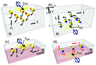
Here we study helicity dependent photocurrent (HDP) in metal/Bi bilayers. The HDP is found to be larger for Ag/Bi bilayer compared to Bi single layer films. Front and back light illuminations are used to separate contributions from the bulk and those associated with interface states, if any. Illustration of the process is described in Fig. 1. For the bulk contributionKawaguchi et al. (2020), the sign of HDP will be the same for front and back illuminations since the direction of spin current, in Figs. 1(a) and 1(b), is the same. In contrast, the spin direction of the electrons present at the bottom surface of Bi (or the metal/Bi interface for metal/Bi bilayers (Fig. 1(c,d))) is opposite for the front and back illuminations. Under such circumstance, interfacial effects (e.g. spin absorption, the inverse Rashba-Edelstein effect (IREE)Sanchez et al. (2013)) can cause current that flows in opposite direction for the two geometries: compare Figs. 1(c) and 1(d). Thus the photocurrent measurements using front and back illuminations allow one to separate bulk and interfacial contributions. We find that the sign of photocurrent reverses for front and back illuminations in Cu/Bi and Ag/Bi bilayers. The magnitude of the photocurrent under back illumination is the largest for Ag/Bi bilayers, indicating that the degree of spin absorption and spin to charge conversion at the interface is the largest.
Metal/Bi bilayers are deposited on silicon or quartz crystal substrates using RF magnetron sputtering. The film structure is sub./seed/ Bi/2 MgO/1 Ta (thickness in nm). We refer to films with and without the seed layer as seed/Bi bilayer and single Bi layer, respectively. The seed layer for the bilayers is 0.5 Ta/2 Cu, 0.5 Ta/2 Ag, 2 W and 0.5 Ta/2 Pt (thickness in nm). The 0.5 nm thick Ta layer is deposited before the seed layer to promote its smooth growth. The 2 MgO/1 Ta layers serve as a capping layer. Wires are formed by inserting a metal shadow mask between the substrate and the sputtering target during the deposition processHirose et al. (2018).
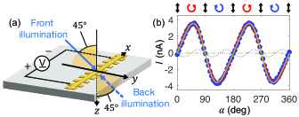
The experimental setup and definition of the coordinate axis are described in Fig. 2(a). Light is irradiated from an oblique angle () to the wire. We refer to front and back illuminations when light is irradiated to the wire from the film side or from the back of the substrate, respectively. The light plane of incidence is always orthogonal to the wire’s long axis. A continuous wave semiconductor laser with wavelength and power is used as the light source. Typical results from nm and mW are presented. The laser spot size is 0.5 mm in diameter. The photovoltage of the wire (width: mm, length: mm) is measured while illuminating light through a quarter wave plate. The angle () of the quarter wave plate’s optical axis with respect to the light plane of incidence defines the light helicity: the light is linearly polarized when , and circularly polarized when (left handed) and (right handed). The photovoltage is converted to photocurrent by dividing the voltage with the resistance of the wire inside the laser spot (0.5 mm long).
Figure 2(b) shows the dependence of the photocurrent from a Ag/Bi bilayer under front illumination. The data is fitted to the following function to extract parameters with different symmetries:
| (1) | ||||
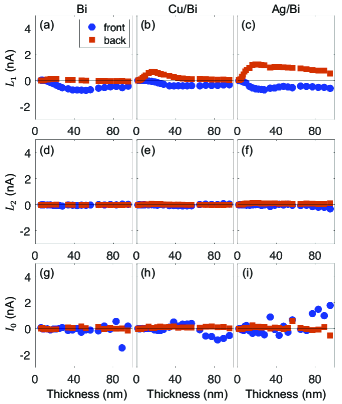
represents photocurrent that depends on the helicity of light, whereas an reflects photocurrent that differs for circularly and linearly polarized lightMcIver et al. (2012); Okada et al. (2016). corresponds to an offset photocurrent that does not depend on and is an offset angle associated with the experimental setup (here ). The fitted curve is shown by the orange solid line in Fig. 2(b), which agrees well with the data. As evident, the photocurrent is dominated by the helicity dependent term (): the other contributions (, and ) are typically smaller than ; see Appendix section I.1 and Fig. 5.
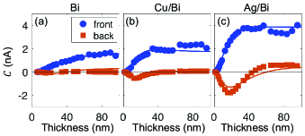
The Bi layer thickness dependence of for Bi single layer, Cu/Bi and Ag/Bi bilayers using front and back light illuminations are shown in Figs. 3(a-c). For front illumination, all structures show an increase in with increasing Bi layer thickness () until it saturates. The saturation value of is the largest for the Ag/Bi bilayer and is the smallest for Bi single layer. For back illumination, is nearly zero for Bi single layer in the entire thickness range studied. Note that in this system (Bi single layer) is also close to zero under front illumination when nm. We infer that the Bi layer within this thickness do not contribute to the generation of light induced spin density, thus forming a spin excitation dead layer possibly due to difference in the structure/texture of Bi. If the thickness of the dead layer, defined as , is close to the light penetration depth, light irradiated from the back of the substrate will not reach a region where a non-zero spin density can be induced, resulting in near zero for back illumination. In contrast, for Cu/Bi and Ag/Bi bilayers, a large negative is found (under back illumination) when is small. increases with increasing and changes its sign from negative to positive when nm. These results show that there are two competing effects that contribute to the generation of HDP in the bilayers.
To model the system, we solve the spin diffusion equation with a source term associated with light induced spin density. We first define the source term. The number of photons absorbed in Bi at position is defined as : correspond to the top surface of the Bi layer in contact with the MgO/Ta capping layer; see Fig. 1(b). We assume the following simplified functional form for :
| (2) |
(For back illumination, substitute for .) is the effective extinction constant and is a coefficient representing the light amplitude for a given Bi layer thickness . In the absence of multiple reflections within the film, is a constant and equals the power of the incident light. Here we take into account multiple reflection and thus depends on .
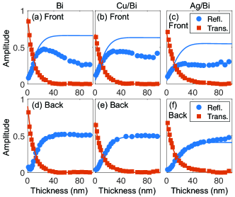
To obtain and , we measure the reflectivity and transmittance of circularly polarized light irradiated to films. The measured and for both front and back illuminations for Bi single layer, Cu/Bi and Ag/Bi bilayers are shown in Appendix Fig. 7. Taking into account multiple reflections that take place at the substrate/film and film/air interfaces (see Appendix section I.2 and Fig. 6), we fit the thickness dependence of and to estimate the refractive index and extinction coefficient of the films. The estimated values of and are shown in Table 1, which are in good agreement with past report on bulk BiWerner et al. (2009).
The absorbance () of a film is expressed as
| (3) |
where is the light power incident on the film. We equate divided by the energy of one photon ( is the speed of light, is the Planck constant) and the area of a laser spot with the thickness integrated sum of , i.e.
| (4) | ||||
Using Eqs. (3) and (4) and and calculated using the experimentally obtained and (see Appendix Eqs. (14) and (16) for the relation between , and , ), we estimate for each . We assume for all samples. Substituting and into Eq. (2), we obtain the number of photons () absorbed at for a given film thickness . For simplicity, we assume one photon absorbed at position in the film generates spin density equivalent of (). Defining as the number of electrons that are spin polarized along the light spin angular momentum, i.e. the spin density, we obtain
| (5) |
We use as the source term of the spin diffusion equation.
The spin diffusion equation is expressed using the chemical potential difference () of the electrons with spin pointing parallel and antiparallel to the light spin angular momentum, that is,
| (6) |
where is the spin diffusion length and is the conductivity of Bi (). We solve Eq. (6) to obtain , which can be converted to spin current density () via the relation,
| (7) |
represents spin current along the -direction with polarization pointing along the light spin angular momentum, which we represent by a unit vector . The boundary condition is defined as
| (8) |
for Bi single layer and
| (9) |
for the seed/Bi bilayers. The seed/Bi interface at is assumed to absorb spin current. The degree of absorbance is characterized by Sanchez et al. (2013). Note that this boundary condition does not explicitly include contributions from, for example, the IREE: it simply describes the presence of an interface that varies the spin current boundary condition. Finally, the ISHE converts the spin current to charge current density ():
| (10) |
where is the spin Hall angle. The total charge current along (), which is measured experimentally, is obtained by integrating the component of over and multiplying (to account for the oblique incidence of light) and the width of the wire.
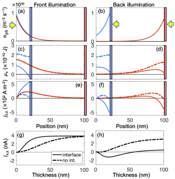
Figures 4(a-f) shows the calculated , and for films with nm (blue lines) and nm (red lines) under front and back illuminations. The solid and dashed lines show results with () and without () a spin absorbing interface, respectively. The difference of the maximum among all conditions shown in Figs. 4(a,b) is due to multiple reflections within Bi. The profiles of and significantly change when the interface is present.
The spin current integrated across the Bi layer thickness, , is plotted as a function of in Figs. 4(g,h). Without the interface (dashed lines), increases with increasing until saturation and is positive for front and back illuminations. With the interface (solid lines), however, the signs of for front and back illuminations are opposite when is small. for back illumination is negative for small and changes its sign a nm. As evident in Fig. 4(f) (see also Fig. 1(c) for a schematic illustration), the presence of spin absorbing interface induces spin current toward the interface. For films with small , is dominated by the back flow toward the interface over contribution from the gradient in spin density (i.e. gradient of ). In addition, for front illumination with the interface is larger compared to that without the interface.
With this model, we fit the experimental results of front and back light illuminations simultaneously, with and used as the fitting parameters. For Cu/Bi and Ag/Bi bilayers, is also varied to fit the data (for Bi single layer, ). A phenomenological spin excitation dead layer () is introduced, which is determined by the thickness which causes near zero for small under front illumination. The calculated are shown by the blue and orange solid lines in Figs. 3(a-c), which show good agreement with the experimental results. The parameters used for the calculations are listed in Table 1.
of Bi obtained here is considerably larger than that of previous reports estimated using spin pumping measurementsHou et al. (2012); Emoto et al. (2016), but is in relatively good agreement with that of sputtered Bi-rich BiSb alloysChi et al. (2020). The estimated of Ag/Bi bilayers is nearly twice as large as that of other structures. The resistivity of Bi in the bilayers studied is similar, suggesting that the spin Hall angle of Bi takes similar valueChi et al. (2020). In the model, we assume the interface modifies the spin current profile in Bi via changes in the boundary condition. The IREESanchez et al. (2013); Nomura et al. (2015); Karube et al. (2016) can convert the spin current that flows into the interface to generate a charge current, providing an additional channel. Interestingly, the size of required to describe the results for Ag/Bi bilayers is close to that reported in similar systemsSanchez et al. (2013). With the current model, however, it is difficult to separate contributions from the ISHE and IREE due to the back flow of spin current to the interface (note that the back flow occurs due to the presence of spin absorbing interface).
| Structure | (nm) | (nm) | (nm) | |||
|---|---|---|---|---|---|---|
| Bi single layer | 0.7 | 18 | 1.3 | 3.2 | N/A | 12 |
| Cu/Bi bilayer | 0.7 | 18 | 1.3 | 3.0 | 6 | 5 |
| Ag/Bi bilayer | 1.4 | 18 | 1.3 | 2.5 | 3 | 1 |
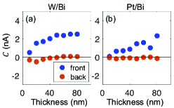
We have also studied photocurrent in W/Bi and Pt/Bi bilayers, in which the seed layer exhibits significantly larger spin Hall effect than Cu and AgHoffmann (2013); Sinova et al. (2015); see Appendix Fig. 8. We find that is not particularly large for these bilayers compared to that of Cu/Bi and Ag/Bi bilayers. As the carrier density of Bi is more than three orders of magnitude smaller than that of typical metals (W and Pt)Kawaguchi et al. (2020), we consider spin current flowing into the seed layer hardly contributes to the charge current within the seed layer via the ISHEFert and Jaffres (2001).
In summary, we have studied bulk and interface contributions to the helicity dependent photocurrent (HDP) in metal/Bi bilayers. As reported previously, the bulk contribution originates from the ISHE of Bi, which converts light induced spin current to charge current within Bi. In metal/Bi bilayers, we find that not only the HDP increases under front illumination, compared to Bi single layer, but also the sign of HDP reverses when light is illuminated from the back. Using a diffusive spin transport model, we show that the metal/Bi interface acts as a strong spin sink and modifies the profile of spin current in Bi. Such change in the spin current profile results in an enhancement of HDP due to the ISHE of Bi as well as the IREE at the interface. We find the largest HDP in Ag/Bi bilayers, both under front and back illuminations, suggesting strong contributions from the interface. These results thus demonstrate means to study spin absorption and spin to charge conversion at interfaces using circularly polarized light. Given that the photocurrent in metal/Bi bilayers is dominated by the helicity dependent component, the large HDP found here can be exploited for polarization sensitive detectors in optical communicationsLiu et al. (2020) as well as light spin angular momentum detectors for quantum opticsTogan et al. (2010).
Acknowledgements.
This work was partly supported by JST CREST (JPMJCR19T3), JSPS Grant-in-Aids (JP15H05702, JP16H03853), Yamada Science Foundation and the Center of Spintronics Research Network of Japan. Y.-C.L. is supported by JSPS International Fellowship for Research in Japan (JP17F17064). H.H. acknowledge financial support from Materials Education program for the future leaders in Research, Industry, and Technology (MERIT).I Appendix
I.1 Helicity and polarization dependent photocurrent
Components of the photocurrent, , and , obtained by fitting the data ( vs. ) with Eq. (1), are shown in Fig. 5 as a function of Bi layer thickness () for Bi single layer, Cu/Bi and Ag/Bi bilayers. In all cases, (see Fig. 3) and show a similar thickness dependence, suggesting that the two effects have a common origin. and are negligible in all structures. For the thicker Bi films, shows relatively large fluctuation, which we consider is related to laser induced heating effects that may originate from the large thermo-electric effects of Bi.
I.2 Multiple reflection model and absorption of light
We calculate the reflectivity and transmittance of the system assuming that multiple reflections takes place at the top and bottom interfaces of the semimetal (Bi) layer. We model the system using three media: air (medium 1), the film including the seed and capping layers (medium 2), and the quartz substrate (medium 3). Since the seed layer and the capping layer are thin compared to the light wavelength, we include them as part of the Bi layer. Note that the Cu and Ag seed layers reduce the amplitude of light transmission. We have measured the light transmission probability () of a 0.5 Ta/2 Cu deposited on quartz crystal and found . We assume 0.5 Ta/2 Ag possesses similar .
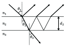
The refractive index of the three media is defined as (air), (film) and (substrate). The thickness of the film is . The other interface of the substrate, substrate/air, is treated as a transmission loss. Transmission loss of the substrate is studied separately using a substrate without the film. The transmission probability is for -polarized light and for -polarized light. Light is irradiated from an oblique angle of . Schematic illustration of the system is shown in Fig. 6.
When a -polarized light with wavelength is incident from medium 1 (air) with an oblique angle on medium 2 (film), the amplitude of the reflected light () and the transmitted light () are
| (11) | ||||
and are the Fresnel reflection and transmission coefficients for -polarized light, defined as
| (12) | ||||
In Eq. (11), , where is the complex refraction angle in the film. The reflection () and transmission () probabilities of the -polarized light are written as
| (13) | ||||
where is the complex refraction angle of the transmitted light in medium 3.
The reflection and transmission probabilities of a circularly polarized light are expressed as
| (14) | ||||
The absorbance of the film for circularly polarized light is calculated as
| (15) |
I.3 Measurements of the optical constants
The optical constants of the films are estimated from measurements of the reflectivity () and transmittance () of circularly polarized light. The measured and for front and back illuminations for Bi single layer, Cu/Bi and Ag/Bi bilayers are shown by the symbols in Figs. 7(a-c) and 7(d-f), respectively. The dependence of and are fitted with Eqs. (14) and (16) to extract and of the film. The extracted values are listed in Table 1. The absorbance are calculated using Eqs. (15) and (17). is equivalent to in Eq. (4).
I.4 Helicity dependent photocurrent for W/Bi and Pt/Bi bilayers
The dependence of for W/Bi and Pt/Bi bilayers are shown in Fig. 8.
References
- Manchon et al. (2019) A. Manchon, J. Zelezny, I. M. Miron, T. Jungwirth, J. Sinova, A. Thiaville, K. Garello, and P. Gambardella, “Current-induced spin-orbit torques in ferromagnetic and antiferromagnetic systems,” Rev. Mod. Phys. 91, 035004 (2019).
- Kimel et al. (2005) A. V. Kimel, A. Kirilyuk, P. A. Usachev, R. V. Pisarev, A. M. Balbashov, and T. Rasing, “Ultrafast non-thermal control of magnetization by instantaneous photomagnetic pulses,” Nature 435, 655 (2005).
- Stanciu et al. (2007) C. D. Stanciu, F. Hansteen, A. V. Kimel, A. Kirilyuk, A. Tsukamoto, A. Itoh, and T. Rasing, “All-optical magnetic recording with circularly polarized light,” Phys. Rev. Lett. 99, 047601 (2007).
- Lambert et al. (2014) C. H. Lambert, S. Mangin, Bsdcs Varaprasad, Y. K. Takahashi, M. Hehn, M. Cinchetti, G. Malinowski, K. Hono, Y. Fainman, M. Aeschlimann, and E. E. Fullerton, “All-optical control of ferromagnetic thin films and nanostructures,” Science 345, 1337 (2014).
- Ganichev et al. (2002) S. D. Ganichev, E. L. Ivchenko, V. V. Bel’kov, S. A. Tarasenko, M. Sollinger, D. Weiss, W. Wegscheider, and W. Prettl, “Spin-galvanic effect,” Nature 417, 153 (2002).
- Ganichev et al. (2004) S. D. Ganichev, V. V. Bel’kov, L. E. Golub, E. L. Ivchenko, P. Schneider, S. Giglberger, J. Eroms, J. De Boeck, G. Borghs, W. Wegscheider, D. Weiss, and W. Prettl, “Experimental separation of rashba and dresselhaus spin splittings in semiconductor quantum wells,” Phys. Rev. Lett. 92, 256601 (2004).
- McIver et al. (2012) J. W. McIver, D. Hsieh, H. Steinberg, P. Jarillo-Herrero, and N. Gedik, “Control over topological insulator photocurrents with light polarization,” Nat. Nanotechnol. 7, 96 (2012).
- Okada et al. (2016) K. N. Okada, N. Ogawa, R. Yoshimi, A. Tsukazaki, K. S. Takahashi, M. Kawasaki, and Y. Tokura, “Enhanced photogalvanic current in topological insulators via fermi energy tuning,” Phys. Rev. B 93, 081403 (2016).
- Pan et al. (2017) Y. Pan, Q. Z. Wang, A. L. Yeats, T. Pillsbury, T. C. Flanagan, A. Richardella, H. J. Zhang, D. D. Awschalom, C. X. Liu, and N. Samarth, “Helicity dependent photocurrent in electrically gated (bi-1-sb-x(x))(2)te-3 thin films,” Nat. Commun. 8, 1037 (2017).
- Yuan et al. (2014) H. T. Yuan, X. Q. Wang, B. Lian, H. J. Zhang, X. F. Fang, B. Shen, G. Xu, Y. Xu, S. C. Zhang, H. Y. Hwang, and Y. Cui, “Generation and electric control of spin-valley-coupled circular photogalvanic current in wse2,” Nat. Nanotechnol. 9, 851 (2014).
- Ma et al. (2017) Q. Ma, S. Y. Xu, C. K. Chan, C. L. Zhang, G. Q. Chang, Y. X. Lin, W. W. Xie, T. Palacios, H. Lin, S. Jia, P. A. Lee, P. Jarillo-Herrero, and N. Gedik, “Direct optical detection of weyl fermion chirality in a topological semimetal,” Nat. Phys. 13, 842 (2017).
- Hirose et al. (2018) H. Hirose, N. Ito, M. Kawaguchi, Y. C. Lau, and M. Hayashi, “Circular photogalvanic effect in cu/bi bilayers,” Appl. Phys. Lett. 113, 222404 (2018).
- Puebla et al. (2019) J. Puebla, F. Auvray, N. Yamaguchi, M. R. Xu, S. Z. Bisri, Y. Iwasa, F. Ishii, and Y. Otani, “Photoinduced rashba spin-to-charge conversion via an interfacial unoccupied state,” Phys. Rev. Lett. 122, 256401 (2019).
- Zutic et al. (2002) I. Zutic, J. Fabian, and S. Das Sarma, “Spin-polarized transport in inhomogeneous magnetic semiconductors: Theory of magnetic/nonmagnetic p-n junctions,” Phys. Rev. Lett. 88, 066603 (2002).
- Endres et al. (2013) B. Endres, M. Ciorga, M. Schmid, M. Utz, D. Bougeard, D. Weiss, G. Bayreuther, and C. H. Back, “Demonstration of the spin solar cell and spin photodiode effect,” Nat. Commun. 4, 2068 (2013).
- Morimoto and Nagaosa (2016) T. Morimoto and N. Nagaosa, “Topological nature of nonlinear optical effects in solids,” Science Advances 2, e1501524 (2016).
- Freimuth et al. (2017) F. Freimuth, S. Blugel, and Y. Mokrousov, “Charge pumping driven by the laser-induced dynamics of the exchange splitting,” Phys. Rev. B 95, 094434 (2017).
- Roca et al. (2017) R. C. Roca, N. Nishizawa, K. Nishibayashi, and H. Munekata, “Investigation of helicity-dependent photocurrent at room temperature from a fe/x-alox/p-gaas schottky junction with oblique surface illumination,” Japanese Journal of Applied Physics 56, 04cn05 (2017).
- Kawaguchi et al. (2020) Masashi Kawaguchi, Hana Hirose, Zhendong Chi, Yong-Chang Lau, Frank Freimuth, and Masamitsu Hayashi, “Giant inverse faraday effect in dirac semimetals,” (2020), arXiv:2009.01388 .
- Pershan et al. (1966) P. S. Pershan, Vanderzi.Jp, and L. D. Malmstrom, “Theoretical discussion of the inverse faraday effect, raman scattering, and related phenomena,” Physical Review 143, 574 (1966).
- Hertel (2006) R. Hertel, “Theory of the inverse faraday effect in metals,” J. Magn. Magn. Mater. 303, L1 (2006).
- Taguchi and Tatara (2011) Katsuhisa Taguchi and Gen Tatara, “Theory of inverse faraday effect in a disordered metal in the terahertz regime,” Phys. Rev. B 84, 174433 (2011).
- Berritta et al. (2016) Marco Berritta, Ritwik Mondal, Karel Carva, and Peter M. Oppeneer, “Ab initio theory of coherent laser-induced magnetization in metals,” Phys. Rev. Lett. 117, 137203 (2016).
- Qaiumzadeh and Titov (2016) A. Qaiumzadeh and M. Titov, “Theory of light-induced effective magnetic field in rashba ferromagnets,” Phys. Rev. B 94, 014425 (2016).
- Freimuth et al. (2016) Frank Freimuth, Stefan Bluegel, and Yuriy Mokrousov, “Laser-induced torques in metallic ferromagnets,” Phys. Rev. B 94, 144432 (2016).
- Tokman et al. (2020) I. D. Tokman, Q. F. Chen, I. A. Shereshevsky, V. I. Pozdnyakova, I. Oladyshkin, M. Tokman, and A. Belyanin, “Inverse faraday effect in graphene and weyl semimetals,” Phys. Rev. B 101, 174429 (2020).
- Saitoh et al. (2006) E. Saitoh, M. Ueda, H. Miyajima, and G. Tatara, “Conversion of spin current into charge current at room temperature: Inverse spin-Hall effect,” Applied Physics Letters 88, 182509 (2006).
- Sanchez et al. (2013) J. C. Rojas Sanchez, L. Vila, G. Desfonds, S. Gambarelli, J. P. Attane, J. M. De Teresa, C. Magen, and A. Fert, “Spin-to-charge conversion using rashba coupling at the interface between non-magnetic materials,” Nat. Commun. 4, 2944 (2013).
- Werner et al. (2009) W. S. M. Werner, K. Glantschnig, and C. Ambrosch-Draxl, “Optical constants and inelastic electron-scattering data for 17 elemental metals,” Journal of Physical and Chemical Reference Data 38, 1013 (2009).
- Hou et al. (2012) D. Z. Hou, Z. Qiu, K. Harii, Y. Kajiwara, K. Uchida, Y. Fujikawa, H. Nakayama, T. Yoshino, T. An, K. Ando, X. F. Jin, and E. Saitoh, “Interface induced inverse spin hall effect in bismuth/permalloy bilayer,” Appl. Phys. Lett. 101, 042403 (2012).
- Emoto et al. (2016) H. Emoto, Y. Ando, G. Eguchi, R. Ohshima, E. Shikoh, Y. Fuseya, T. Shinjo, and M. Shiraishi, “Transport and spin conversion of multicarriers in semimetal bismuth,” Phys. Rev. B 93, 174428 (2016).
- Chi et al. (2020) Zhendong Chi, Yong-Chang Lau, Xiandong Xu, Tadakatsu Ohkubo, Kazuhiro Hono, and Masamitsu Hayashi, “The spin hall effect of bi-sb alloys driven by thermally excited dirac-like electrons,” Science Advances 6, eaay2324 (2020).
- Nomura et al. (2015) A. Nomura, T. Tashiro, H. Nakayama, and K. Ando, “Temperature dependence of inverse rashba-edelstein effect at metallic interface,” Appl. Phys. Lett. 106, 212403 (2015).
- Karube et al. (2016) S. Karube, K. Kondou, and Y. Otani, “Experimental observation of spin-to-charge current conversion at non-magnetic metal/bi2o3 interfaces,” Appl. Phys. Express 9, 033001 (2016).
- Hoffmann (2013) Axel Hoffmann, “Spin hall effects in metals,” IEEE Trans. Magn. 49, 5172 (2013).
- Sinova et al. (2015) Jairo Sinova, Sergio O. Valenzuela, J. Wunderlich, C. H. Back, and T. Jungwirth, “Spin hall effects,” Rev. Mod. Phys. 87, 1213–1259 (2015).
- Fert and Jaffres (2001) A. Fert and H. Jaffres, “Conditions for efficient spin injection from a ferromagnetic metal into a semiconductor,” Phys. Rev. B 64, 184420 (2001).
- Liu et al. (2020) Jing Liu, Fengnian Xia, Di Xiao, F. Javier Garcia de Abajo, and Dong Sun, “Semimetals for high-performance photodetection,” Nat. Mater. 19, 830 (2020).
- Togan et al. (2010) E. Togan, Y. Chu, A. S. Trifonov, L. Jiang, J. Maze, L. Childress, M. V. G. Dutt, A. S. Sorensen, P. R. Hemmer, A. S. Zibrov, and M. D. Lukin, “Quantum entanglement between an optical photon and a solid-state spin qubit,” Nature 466, 730 (2010).