Polarization-controlled selective excitation of Mie resonances of dielectric nanoparticle on a coated substrate
Abstract
Spherical high-index nanoparticles with low material losses support sharp high-Q electric and magnetic resonances and exhibit a number of interesting optical phenomena. Developments in fabrication techniques have enabled further study of their properties and the investigation of related optical effects. After deposition on a substrate, the optical properties of a particle change dramatically due to mutual interaction. Here, we consider a silicon spherical nanoparticle on a dielectric one-layered substrate. At normal incidence of light, the layer thickness controls the contribution of the nanoparticle’s electric and magnetic multipoles to the subsequent optical response. We show that changing the polarization of incident light at a specific excitation angle and layer thickness leads to switching between the multipoles. We further observe a related polarization-driven control over the direction of the scattered radiation.
I Introduction
Plasmonic and high-index dielectric resonant nanoparticles are one of the key building blocks in modern nanophotonics Krasnok et al. (2012); Giannini et al. (2011). They offer efficient control over light at the nanoscale whether single or packed in an array, and have a number of applications Jahani and Jacob (2016); Aieta et al. (2015); Miroshnichenko and Kivshar (2012); Evlyukhin et al. (2010). For example, plasmonic nanoparticles exhibit strong field localization Hutter and Fendler (2004); Maier (2007), and are used for SERS Dornhaus et al. (1980); Alvarez-Puebla et al. (2007), sensing Melendez et al. (1996); Taylor and Zijlstra (2017), as well as for chemical and biological applications Meyerbröker et al. (2013); Brolo (2012). However, the high intrinsic losses of plasmonic materials limit their use for certain applications. High-index dielectric nanoparticles, on the other hand, have significantly lower losses and support both electric and magnetic responses in the visible and near-IR regions Kuznetsov et al. (2012); Staude et al. (2013). This leads to several new phenomena such as Kerker effect Nieto-Vesperinas et al. (2011); Liu and Kivshar (2018); Alaee et al. (2015), directional scattering Shamkhi et al. (2019); Lu et al. (2015); Liu and Kivshar (2018) or excitation of surface plasmon-polariton Sinev et al. (2017, 2020). Finally, dielectric nanoparticles have enabled many non-liner photonic effects Shcherbakov et al. (2014); Makarov et al. (2015); Shcherbakov et al. (2015); Carletti et al. (2019); Koshelev et al. (2020), implementation of subwavelength room-temperature lasers Tiguntseva et al. (2020).
The optical properties of spherical nanoparticles are described by Mie theory Bohren and Huffman (2008); Kerker (2013), where high-index dielectric nanoparticles exhibit pronounced optical resonances. Their fundamental mode (with the lowest frequency) is a magnetic dipole (MD) resonance, followed by an electric dipole (ED), a magnetic quadrupole (MQ), and so on into higher-order multipoles. Mie theory predicts the spectral position and quality factor for each multipole separately, but there is some overlap of multipoles and several multipoles are excited at the same wavelength. In some cases, selective excitation of multipoles is necessary Van de Groep and Polman (2013); Koshelev et al. (2020), such as the selective excitation of MD to enhance second Carletti et al. (2015) and third harmonic generation Melik-Gaykazyan et al. (2017). Another example is the enlarged optical pulling and pushing forces Liu et al. (2017) caused by manipulation of the ED, MD, and MQ of the dielectric nanoparticles. Finally, control over the contribution of multipoles to scattering provides multicolor pixels at the nanoscale Nagasaki et al. (2017); Flauraud et al. (2017); Xiang et al. (2018); Li et al. (2019).
There are a number of methods for the selective excitation of multipole resonances of high-index particles. One of them is structured light in the form of tightly focused cylindrical vector-beams Woźniak et al. (2015). Alternatively, radially polarized light Neugebauer et al. (2016) or even a simple plane wave excitation Xiang et al. (2018); Sinev et al. (2016); Van de Groep and Polman (2013) are also possible. An efficient way to control multipoles was proposed by Xiang et al. Xiang et al. (2018), where the authors suggested using the evanescent field for excitation by illuminating the nanoantenna from the substrate side under the total internal reflection condition. Here, we use far-field excitation, which is more practical. Sinev et al. in Ref. Sinev et al. (2016) demonstrated the polarization-controlled enhancement of the MD of a silicon nanoparticle on a plasmonic substrate. Alternatively, Van de Groep and Polman Van de Groep and Polman (2013) showed theoretically that a dielectric one-layered substrate can be used to control ED and MD contribution to the scattering. However, they only considered the case of normal incidence, where due to the selection rules, only modes with the azimuthal number were present. In term of the group symmetry, one can say that only the modes from irreducible representation were excited Gladyshev et al. (2020).
Here, we use oblique incident light, which contains all azimuthal harmonics and, thus, excites the modes with, m=. It gives an additional degree of freedom for selective multipole excitation and manipulation of their interference. We show that the angle of incidence and polarization of the excitation light combined with adjusting the silica spacer, which separates the nanoantenna from the silicon substrate provide a flexible control over the relative amplitudes of MD and ED, and their interference which governs the scattered field. The thickness of the SiO2 spacer defines the phase shift between ED and MD, while the incident angle defines their relative amplitudes. Thus, we can strongly enhance or almost completely suppress the ED or MD component in the scattered field or maximize the scattering in certain directions. For example, the demonstrated enhancement of scattering to the directions of light source can be used for retroreflectors of subwavelength thickness Arbabi et al. (2017).
II Results and discussion
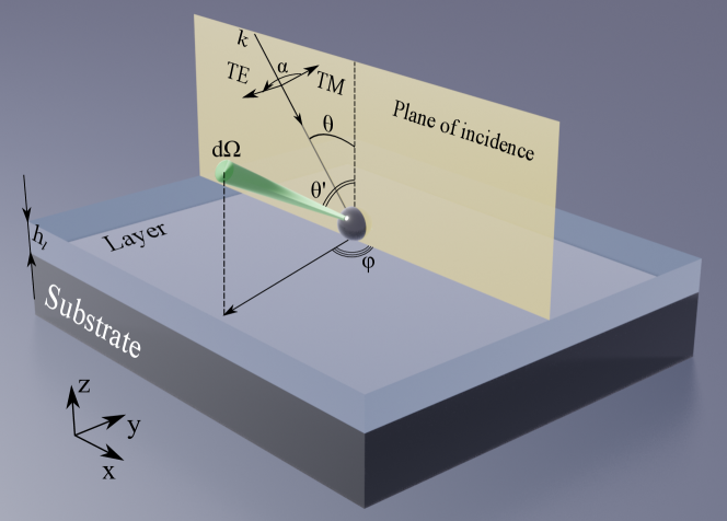
We consider scattering from a silicon spherical nanoparticle with fixed radius nm on top of a silica layer of variable thickness backed by the silicon substrate (see Fig. 1). We employ the T-matrix method for scattering from a single particle and the scattering matrix method for propagation in a layered structure. These methods have previously been implemented in open-source numerical software “Smuthi” using Python Egel et al. (2016a, b, 2017). Simulation of the electromagnetic fields inside the particle was performed in COMSOL Multiphysics package.
‘
It is important to note that an analytical solution of the scattering problem for a small dielectric or plasmonic particle can be indeed obtained even for the case of multilayered substrate and oblique incident plane wave in a point-dipole approximation using the Green’s function formalism Miroshnichenko et al. (2015). We used this method, for example, in Sinev et al. (2017, 2020). However, the analytical solutions are quite cumbersome for the analysis as it requires calculation of Sommerfeld’s integral and solutions of a transcendent equation for complex poles of the leaky modes. Therefore, the numerical analysis is almost unavoidable. Moreover, in Sec. II.C we analyzed the directivity of the scattered field taking into account magnetic quadrupole resonance. These regimes are beyond the dipole approximation and also require numerical calculations for the correct analysis of scattering. Finally, the analytical solution in a point-dipole approximation contains a fitting parameter — the height at which the point dipole should be positioned. The scattering from the nanoantenna strongly depends on this parameter (see additional materials to Miroshnichenko et al. (2015)).
II.1 Normal incidence
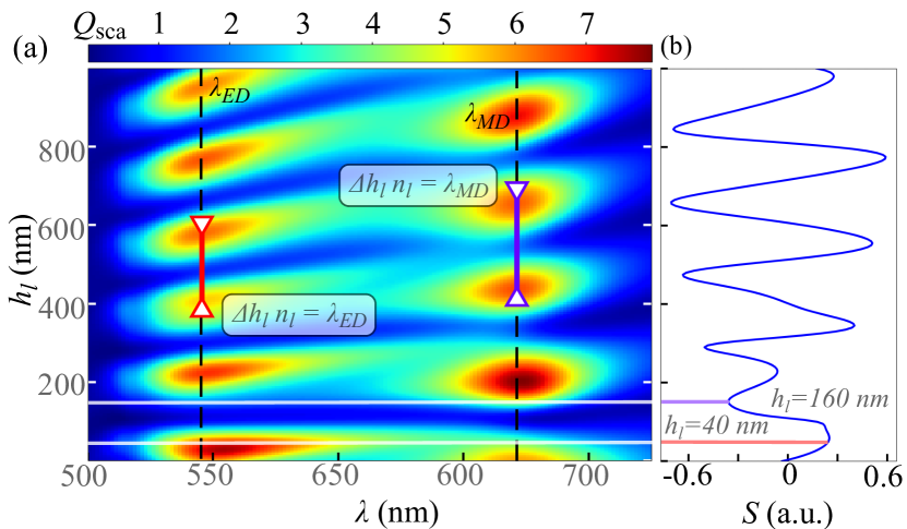
Firstly, varying the thickness of the layer hl, we investigate the upper half-space scattering efficiency Qsca at normal incidence, where scattering efficiency is a scattering cross-section normalized to a geometrical cross-section.
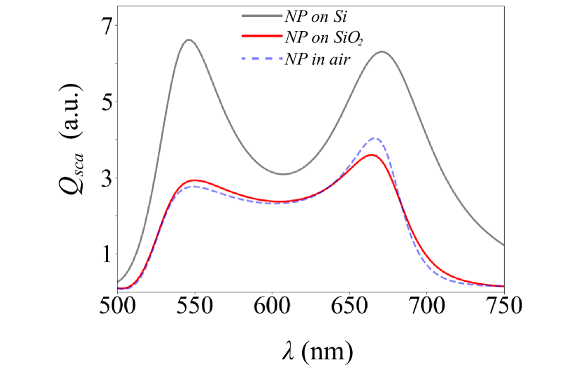
At zero hl, with the particle located on a silicon substrate, the scattering is enhanced in comparison with the free space case. In spite the interaction with the substrate, there is no spectral shift of the ED and MD resonances (see Appendix A, Fig. 9). Infinite hl corresponds to the case of a particle on glass, where the scattering enhancement is negligible. For intermediate cases, the layer modulates the standing wave in the upper half-space, that results in scattering modulation (see Fig. 2a). As MD (at 670 nm) and ED (at 540 nm) interact with the standing wave, along the hl axis we note oscillating behavior of the Qsca with a resonant condition:
| (1) |
where nl is a refractive index of the layer, m is an integer, and is associated with initial scattering phase. The presence of the initial scattering phase, which is different for the ED and MD, makes it possible to find layer thicknesses where simultaneous enhancement or suppression of both dipoles occurs (see Fig. 3a). Alternatively, dipole enhancement takes place at different layer thicknesses. For example, enhancement of the ED can be achieved at h nm, and of the MD at h nm (see Fig. 3b and 3c).

In order to quantify the relative contributions of dipoles, we introduce selectivity, defined as:
| (2) |
where and are scattering efficiencies at wavelengths of the ED and MD resonances (see Fig. 2b). At thicknesses of 40 nm and 160 nm, the selectivity is 0.23 and -0.36, respectively. In these states, we provide the fit of Qsca by two Fano-like curves to represent the ED and MD contribution (thin red and blue dashed lines in Figs. 3b and 3c). For example, at the wavelength of the enhanced ED, the contribution of the suppressed MD to the scattering efficiency is negligible (see Fig. 3b), the enhanced MD effect being similar. The dominance of one dipole over another also appears as a characteristic pattern in the field distribution inside the particle (see inserts in Fig 3b and c). It should be noted that the absolute value of the selectivity is relatively small due to the overlapping of the enhanced and suppressed
dipoles at the wavelength of the latter. As we further increase the layer thickness, the selectivity oscillates, reaching extreme values of 0.6 and -0.7 (see Fig. 2b). At the same time, these values do not reflect the presence of the additional spectral features associated with Fabri-Perot modes in thick layers. We have to therefore use additional degrees of freedom in order to achieve a regime where only one dipole contributes to the scattering.
II.2 Oblique incidence
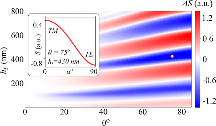
A single-dipole scattering regime can be achieved at an oblique incidence. In this case, the polarization of the incident radiation begins to play a significant role, allowing us to switch selectivity while keeping the angle of incidence and the thickness of the layer constant. In order to find the optimal values for the incidence angle, as well as the thickness of the layer, we simulate the
difference between selectivity for TE and TM polarization at different incidence angle and buffer layer thickness:
| (3) |
where and are selectivity values for TE and TM incident polarization.As far as the selectivity itself
is an analog to the contrast between the contributions of electric and magnetic dipoles to scattering, the selectivity variation allows to determine the parameters that simultaneously achieve single-dipole scattering regimes and pronounced polarization-driven switching between them. Therefore, scattering efficiencies at ED and MD resonant wavelengths for both polarization are used for Fig.4. There we see that the absolute value of selectivity variation grows with the increase of the incidence angle, while the dependence on the layer thickness is periodic in character.
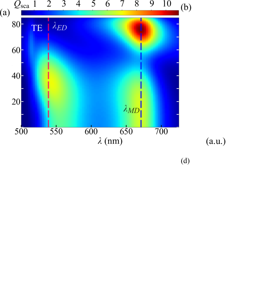
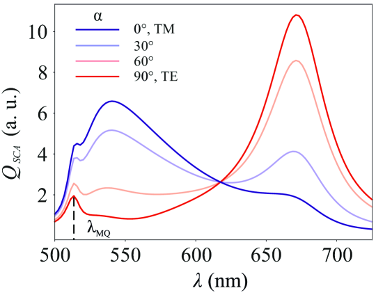
Next, we demonstrate polarization switching of the selectivity with layer thickness equals 430 nm, and an incident angle of 75∘ (white dot in Fig. 4). Scattering efficiency maps of wavelength-incident angle coordinates for both TE and TM polarization are shown in Figs. 5a and 5c. At normal incidence, the ED and MD make approximately equal contribution to scattering, which remains the same for both polarizations as the angle of incidence increases. However, in the vicinity of 75∘, single-ED or single-MD scattering regimes occur. Figure. 5a shows that, for TE polarization, the enhanced MD almost completely dominates the suppressed ED, a situation which is reversed with TM polarization (see Fig. 5c).
We explain this effect by considering the angular dependence of the background field of the standing wave at wavelengths of the ED and MD in plane where coincides with the upper boundary of the layer. We calculate normalized fields using Fresnel coefficients then choose the determining components of the fields. In the case of TE polarization (see Fig. 5b), Ey() has a maximum at 30∘ and then subsides, while Hz() reaches its maximum at 70∘. Since the magnitude of the dipole is proportional to the applied field, the vertical magnetic dipole provides most of the scattering, so the MD-only scattering regime is achieved.
Additionally, due to suppression of the ED it becomes possible to distinguish the MQ contribution to scattering, dashed line in Fig. 6, TE polarization. The ED-only scattering regime for TM polarization occurs similarly. Changing the polarization angle from TE to TM, we can continuously tune the scattering regime from MD-only to ED-only (see Fig. 6 and inset in Fig. 4).
.
II.3 Directivity of scattered radiation
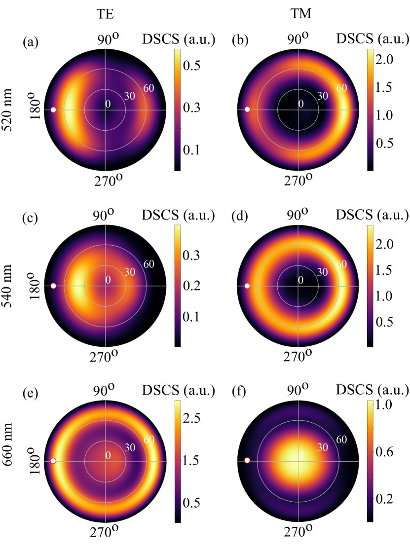
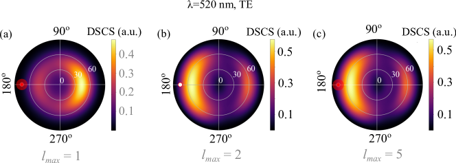
In the previous section we found an angle of incidence and layer thickness that enabled us tune the scattering regimes in the upper half-space. The contribution of three main features, the MQ, MD, and ED, is controlled by the polarization direction of the excitation. In this section, we investigate the directivity of scattered radiation in peculiar regimes. In the upper half-space we simulate the differential scattering cross-section (DSCS) normalized to the geometrical cross-section of the particle. The most distinctive patterns are plotted in Fig. 7 in polar coordinates. The polar angle of the scattered radiation is plotted along the radial coordinate. The azimuthal angle increases in a counterclockwise direction. The direction of the incident radiation with = 75∘ and = 180∘ is indicated by the dots in Fig. 7.
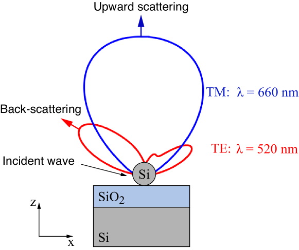
The first regime of interest occurs in the vicinity of the MQ, at = 520 nm, TE polarization. While the contribution of the ED is vastly suppressed for TE-polarized excitation, the MQ begins to noticeably affect the DSCS pattern. Interference between radiation scattered by the ED and the MQ results in negative-angle scattering (see Fig. 7a), which is plotted by a red curve in Fig. 8, where the directivity pattern is plotted in the plane of incidence (-plane). It should be noted that if we only consider ED and MD in the simulation, negative-angle scattering disappears (see Appendix B, Fig. 10). Switching the polarization to TM significantly increases the contribution of the ED, and a dipole-like DSCS with small asymmetry is achieved (see Fig. 7b). The pattern becomes symmetric at the wavelength of the ED resonance (see Fig. 7d), and similarly at a wavelength of , TE polarization (see Fig. 7e). Switching polarization back to TM, we suppress the MD and the contributions of both dipoles become comparable, leading to directional upward scattering (see Fig. 7f and Fig. 8, blue curve).
III Conclusion
In this article we show that a one-layered substrate is an effective platform for the manipulation of resonances of a dielectric nanoparticle. At normal incidence, the thickness of the layer controls the enhancement and suppression of the ED and the MD. At oblique incidence, it becomes possible to control the contribution of the ED and the MD to the optical response through polarization of the incident light. We futher present conditions where one dipole resonance is almost completely suppressed as the other is enhanced, and where a smooth transition to the reverse is also possible. Finally, we present negative angle and upward scattering regimes, and show that adjusting the ED and the MD contributions controls directivity of scattered radiation.
IV Acknowledgement
This work is supported by RFBR, project number 18-29-20063. The multipole expansion calculations are supported by RFBR (19-02-00419). The Authors acknowledge Ian Dick for proofreading.
Appendix A: Comparison of scattering efficiencies for the nanoparticle on different substrates
Here, we simulate scattering efficiency in the upper half space of a spherical silicon nanoparticle with the radius nm, placed in the air, on silicon and glass substrate. On the silicon substrate the scattering is enhanced in comparison with the free space case with no spectral shift of the ED and MD resonances. For the particle on the glass scattering enhancement is negligible.
Appendix B: Modification of the differential scattering cross section pattern
In order to show, that the negative angle scattering occurs due to the interference between radiation scattered by the ED and the MQ, we simulated DSCS for the silicon nanoparticle on one-layered substrate, with the parameters given in the article, taking into account different maximal order of multipoles. In S 2(a) it is seen, that considering only dipole terms, we don’t have negative angle scattering. Taking into account quadrupole, we obtain negative angle scattering. Further increase of the maximal order of multipoles, the DSCS pattern doesn’t change.
References
- Krasnok et al. (2012) A. E. Krasnok, A. E. Miroshnichenko, P. A. Belov, and Y. S. Kivshar, Opt. Express 20, 20599 (2012).
- Giannini et al. (2011) V. Giannini, A. I. Fernández-Domínguez, S. C. Heck, and S. A. Maier, Chem. Rev. 111, 3888 (2011).
- Jahani and Jacob (2016) S. Jahani and Z. Jacob, Nat. Nanotechnol. 11, 23 (2016).
- Aieta et al. (2015) F. Aieta, M. A. Kats, P. Genevet, and F. Capasso, Science 347, 1342 (2015).
- Miroshnichenko and Kivshar (2012) A. E. Miroshnichenko and Y. S. Kivshar, Nano Lett. 12, 6459 (2012).
- Evlyukhin et al. (2010) A. B. Evlyukhin, C. Reinhardt, A. Seidel, B. S. Luk’yanchuk, and B. N. Chichkov, Phys. Rev. B 82, 045404 (2010).
- Hutter and Fendler (2004) E. Hutter and J. H. Fendler, Adv. Mater. 16, 1685 (2004).
- Maier (2007) S. A. Maier, Plasmonics: fundamentals and applications (Springer Science & Business Media, 2007).
- Dornhaus et al. (1980) R. Dornhaus, R. E. Benner, R. K. Chang, and I. Chabay, Surf. Sci. 101, 367 (1980).
- Alvarez-Puebla et al. (2007) R. Alvarez-Puebla, B. Cui, J.-P. Bravo-Vasquez, T. Veres, and H. Fenniri, J. Phys. Chem. C 111, 6720 (2007).
- Melendez et al. (1996) J. Melendez, R. Carr, D. U. Bartholomew, K. Kukanskis, J. Elkind, S. Yee, C. Furlong, and R. Woodbury, Sens. Actuator B-Chem. 35, 212 (1996).
- Taylor and Zijlstra (2017) A. B. Taylor and P. Zijlstra, ACS Sensors 2, 1103 (2017).
- Meyerbröker et al. (2013) N. Meyerbröker, T. Kriesche, and M. Zharnikov, ACS Appl. Mater. Interfaces 5, 2641 (2013).
- Brolo (2012) A. G. Brolo, Nat. Photonics 6, 709 (2012).
- Kuznetsov et al. (2012) A. I. Kuznetsov, A. E. Miroshnichenko, Y. H. Fu, J. Zhang, and B. Luk’Yanchuk, Sci. Rep. 2, 492 (2012).
- Staude et al. (2013) I. Staude, A. E. Miroshnichenko, M. Decker, N. T. Fofang, S. Liu, E. Gonzales, J. Dominguez, T. S. Luk, D. N. Neshev, I. Brener, et al., ACS Nano 7, 7824 (2013).
- Nieto-Vesperinas et al. (2011) M. Nieto-Vesperinas, R. Gomez-Medina, and J. Saenz, JOSA A 28, 54 (2011).
- Liu and Kivshar (2018) W. Liu and Y. S. Kivshar, Opt. Express 26, 13085 (2018).
- Alaee et al. (2015) R. Alaee, R. Filter, D. Lehr, F. Lederer, and C. Rockstuhl, Opt. Lett. 40, 2645 (2015).
- Shamkhi et al. (2019) H. K. Shamkhi, K. V. Baryshnikova, A. Sayanskiy, P. Kapitanova, P. D. Terekhov, P. Belov, A. Karabchevsky, A. B. Evlyukhin, Y. Kivshar, and A. S. Shalin, Phys. Rev. Lett. 122, 193905 (2019).
- Lu et al. (2015) G. Lu, Y. Wang, R. Y. Chou, H. Shen, Y. He, Y. Cheng, and Q. Gong, Laser Photonics Rev. 9, 530 (2015).
- Sinev et al. (2017) I. S. Sinev, A. A. Bogdanov, F. E. Komissarenko, K. S. Frizyuk, M. I. Petrov, I. S. Mukhin, S. V. Makarov, A. K. Samusev, A. V. Lavrinenko, and I. V. Iorsh, Laser Photonics Rev. 11, 1700168 (2017).
- Sinev et al. (2020) I. Sinev, F. Komissarenko, I. Iorsh, D. Permyakov, A. Samusev, and A. Bogdanov, ACS Photonics 7, 680 (2020).
- Shcherbakov et al. (2014) M. R. Shcherbakov, D. N. Neshev, B. Hopkins, A. S. Shorokhov, I. Staude, E. V. Melik-Gaykazyan, M. Decker, A. A. Ezhov, A. E. Miroshnichenko, I. Brener, et al., Nano Lett. 14, 6488 (2014).
- Makarov et al. (2015) S. Makarov, S. Kudryashov, I. Mukhin, A. Mozharov, V. Milichko, A. Krasnok, and P. Belov, Nano Lett. 15, 6187 (2015).
- Shcherbakov et al. (2015) M. R. Shcherbakov, P. P. Vabishchevich, A. S. Shorokhov, K. E. Chong, D.-Y. Choi, I. Staude, A. E. Miroshnichenko, D. N. Neshev, A. A. Fedyanin, and Y. S. Kivshar, Nano Lett. 15, 6985 (2015).
- Carletti et al. (2019) L. Carletti, S. S. Kruk, A. A. Bogdanov, C. De Angelis, and Y. Kivshar, Phys. Rev. Research 1, 023016 (2019).
- Koshelev et al. (2020) K. Koshelev, S. Kruk, E. Melik-Gaykazyan, J.-H. Choi, A. Bogdanov, H.-G. Park, and Y. Kivshar, Science 367, 288 (2020).
- Tiguntseva et al. (2020) E. Tiguntseva, K. Koshelev, A. Furasova, P. Tonkaev, V. Mikhailovskii, E. V. Ushakova, D. G. Baranov, T. Shegai, A. A. Zakhidov, Y. Kivshar, et al., ACS Nano (2020).
- Bohren and Huffman (2008) C. F. Bohren and D. R. Huffman, Absorption and scattering of light by small particles (John Wiley & Sons, 2008).
- Kerker (2013) M. Kerker, The scattering of light and other electromagnetic radiation: physical chemistry: a series of monographs, Vol. 16 (Academic Press, 2013).
- Van de Groep and Polman (2013) J. Van de Groep and A. Polman, Opt. Express 21, 26285 (2013).
- Carletti et al. (2015) L. Carletti, A. Locatelli, O. Stepanenko, G. Leo, and C. De Angelis, Opt. Express 23, 26544 (2015).
- Melik-Gaykazyan et al. (2017) E. V. Melik-Gaykazyan, S. S. Kruk, R. Camacho-Morales, L. Xu, M. Rahmani, K. Zangeneh Kamali, A. Lamprianidis, A. E. Miroshnichenko, A. A. Fedyanin, D. N. Neshev, et al., ACS Photonics 5, 728 (2017).
- Liu et al. (2017) H. Liu, M. Panmai, Y. Peng, and S. Lan, Opt. Express 25, 12357 (2017).
- Nagasaki et al. (2017) Y. Nagasaki, M. Suzuki, and J. Takahara, Nano Lett. 17, 7500 (2017).
- Flauraud et al. (2017) V. Flauraud, M. Reyes, R. Paniagua-Dominguez, A. I. Kuznetsov, and J. Brugger, ACS Photonics 4, 1913 (2017).
- Xiang et al. (2018) J. Xiang, J. Li, Z. Zhou, S. Jiang, J. Chen, Q. Dai, S. Tie, S. Lan, and X. Wang, Laser Photonics Rev. 12, 1800032 (2018).
- Li et al. (2019) S.-Q. Li, X. Xu, R. M. Veetil, V. Valuckas, R. Paniagua-Domínguez, and A. I. Kuznetsov, Science 364, 1087 (2019).
- Woźniak et al. (2015) P. Woźniak, P. Banzer, and G. Leuchs, Laser Photonics Rev. 9, 231 (2015).
- Neugebauer et al. (2016) M. Neugebauer, P. Woźniak, A. Bag, G. Leuchs, and P. Banzer, Nat. Commun. 7, 1 (2016).
- Sinev et al. (2016) I. Sinev, I. Iorsh, A. Bogdanov, D. Permyakov, F. Komissarenko, I. Mukhin, A. Samusev, V. Valuckas, A. I. Kuznetsov, B. S. Luk’yanchuk, et al., Laser Photonics Rev. 10, 799 (2016).
- Gladyshev et al. (2020) S. Gladyshev, K. Frizyuk, and A. Bogdanov, Phys. Rev. B 102, 075103 (2020).
- Arbabi et al. (2017) A. Arbabi, E. Arbabi, Y. Horie, S. M. Kamali, and A. Faraon, Nat. Photonics 11, 415 (2017).
- Egel et al. (2016a) A. Egel, S. W. Kettlitz, and U. Lemmer, JOSA A 33, 698 (2016a).
- Egel et al. (2016b) A. Egel, D. Theobald, Y. Donie, U. Lemmer, and G. Gomard, Opt. Express 24, 25154 (2016b).
- Egel et al. (2017) A. Egel, Y. Eremin, T. Wriedt, D. Theobald, U. Lemmer, and G. Gomard, J. Quant. Spectrosc. Radiat. Transfer 202, 279 (2017).
- Miroshnichenko et al. (2015) A. E. Miroshnichenko, A. B. Evlyukhin, Y. S. Kivshar, and B. N. Chichkov, ACS Photonics 2, 1423 (2015).