Edge photocurrent in bilayer graphene due to inter-Landau-level transitions
Abstract
We report the observation of the resonant excitation of edge photocurrents in bilayer graphene subjected to terahertz radiation and a magnetic field. The resonantly excited edge photocurrent is observed for both inter-band (at low carrier densities) and intra-band (at high densities) transitions between Landau levels (LL). While the intra-band LL transitions can be traced to the classical cyclotron resonance (CR) and produce strong resonant features, the inter-band-LL resonances have quantum nature and lead to the weaker features in the measured photocurrent spectra. The magnitude and polarization properties of the observed features agree with the semiclassical theory of the intra-band edge photogalvanic effect, including its Shubnikov-de-Haas oscillations at low temperatures.
I Introduction
The electronic and transport properties of graphene and two-dimensional (2D) semiconductors are strongly dependent on properties of the systems edges. Prominent examples are the quantum Hall regime v. Klitzing et al. (1980); Halperin (1982); Sarma and Pinczuk (1997); Novoselov et al. (2006); Neto et al. (2009), the spin Hall effect in 2D topological insulators Murakami et al. (2004); Kane and Mele (2005); Bernevig and Zhang (2006); König et al. (2007); Hasan and Kane (2010); Qi and Zhang (2011), or quantum valley Hall effects in chiral edge states Neto et al. (2009); Martin et al. (2008); Yao et al. (2009); Zhang et al. (2011); Jung et al. (2011); Vaezi et al. (2013). In general, the energy dispersion and masses of the edge charge carriers can substantially differ from those of the material bulk. Thus, experimental access to these fundamental material properties becomes important. Different experimental techniques have been employed to explore electronic properties of edges including measurements of the quantum Hall effect Sanchez-Yamagishi et al. (2016), scanning tunneling microscopy (STM) Niimi et al. (2006); Ritter and Lyding (2009); Yin et al. (2016), spatially resolved Raman scattering Casiraghi et al. (2009); Heydrich et al. (2010); Begliarbekov et al. (2010), spin Hall effect in topological insulator systems König et al. (2007), imaging of edge currents by superconducting quantum interference devices (SQUID) Nowack et al. (2013); Marguerite et al. (2019), electron spin resonance Slota et al. (2018), high-resolution transmission electron microscopy (TEM) Liu et al. (2009), and near-field infrared nanometre-scale microscopy (nanoscopy) Ju et al. (2015); Fei et al. (2015); Jiang et al. (2016); Nikitin et al. (2016); Li et al. (2016). In the last decade it has been demonstrated that an access to the spin/valley properties of the edge transport can be obtained employing edge photogalvanic currents excited by terahertz or infrared radiation Karch et al. (2011); Glazov and Ganichev (2014); Dantscher et al. (2017); Luo and Li (2017); Ganichev et al. (2017); Xu et al. (2018); Plank et al. (2018); Durnev and Tarasenko (2019); Candussio et al. (2020); Otteneder et al. (2020). While detection and analysis of the cyclotron resonance at the edges vicinity would provide an informative and important tool to study such edge properties as the energy spectrum, cyclotron mass, carrier density (type), and relaxation times, this challenging goal is missing so far. These data can also be useful in the development of novel graphene-based THz detectors, see e.g. Refs Vicarelli et al. (2012); Freitag et al. (2013); Koppens et al. (2014); Olbrich et al. (2016); Auton et al. (2016, 2017); Bandurin et al. (2018); Castilla et al. (2019); Delgado-Notario et al. (2020).
Here, we report on the observation of resonantly enhanced edge photogalvanic currents which probe magnetotransport in nanometers-scale vicinity of the edges. The effect is demonstrated in high-mobility m-scale bilayer graphene structures excited by THz radiation. The peaks in the edge current are caused by absorption peaks at frequencies that match the energies of either intra-band or inter-band Landau level (LL) transitions subjected to selection rules and favorable LL occupancy. The stronger intra-band peaks correspond to classical cyclotron resonances (CRs), while the weaker inter-band resonances have no classical counterpart. Below, we loosely refer to all the observed peaks as “CR”, making clear identification of their origin.
The observed photocurrent flows along the sample edges and its direction is defined by the magnetic field polarity. Upon variation of the magnetic field the edge current behaviour follows the semiclassical shape of the CR in the absorbance. Our analysis of the positions and shape of the CR resonances shows that properties of the edges in studied bilayer graphene samples can be well described by parameters of the material bulk. Depending on the carrier density the resonances are caused by either inter-band or intra-band transitions between lowest Landau levels at low carrier density or involves transitions between adjacent LL in the conduction band in the semiclassical regime at high carrier density. In the latter case the resonant edge photogalvanic current additionally exhibits Shubnikov-de-Haas effect related -periodic magnetooscillations yielding information on the edge carrier density. Rotating the polarization plane of normally incident THz radiation we observed that the orientation of the radiations electric field vector only slightly affects the photocurrent amplitude. The developed microscopic theory of the edge photocurrent in semiclassical regime is based on Boltzmann’s kinetic equation and is in a good agreement with the experiment. The effect described here is probed in bilayer graphene; we note, however, that it is of general nature and should be observable also in other two-dimensional crystalline systems like monolayer graphene, 2D topological insulators, and transition metal dichalcogenide monolayers.
II Samples and methods
The experiments reported in this paper were carried out on Hall bar structures prepared from exfoliated bilayer graphene, encapsulated in hexagonal boron nitride and equipped with a back gate. We confirmed the bilayer nature of our graphene sample using Raman spectroscopy and low-temperature magnetotransport. Briefly, the spectra show a single sharp G peak at 1576 cm-1 and a broad asymmetric 2D band with features typical for bilayer graphene Lee et al. (2011), for further details see Appendix 1. (290 nm)/Si serves as sample substrate and the contacts are made of Cr(3 nm)/Au. Figure 1(a) shows a picture of the Hall bar structure, with dimensions . The gate voltage dependence of the longitudinal resistance presented in Figure 1(c) demonstrates a clear charge neutrality point (CNP). The curve was obtained in the absence of THz radiation applying a current of modulated with a frequency of . The CNP slightly shifts for different cool downs, therefore, we introduce an effective gate voltage . The carrier density as a function of the effective gate voltage obtained from magnetotransport experiments is presented in the inset of Fig. 1. The field effect mobility on the hole side is cm2/Vs and on the electron side it is cm2/Vs. More details on the transport and magnetotransport data are given in the Appendix 1.
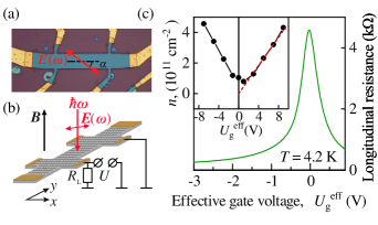
A continuous wave (cw) optically pumped molecular laser served as source of the normal incident THz radiation exciting the photocurrents with frequencies of THz (wavelength m, photon energy meV) and THz (m, meV) Ganichev et al. (1982); Olbrich et al. (2013); Plank et al. (2016). These laser lines were obtained using methanol and difluormethane as active media, respectively. A pyroelectric detector was used to control the radiation power on the sample mW. The beam cross-section monitored by a pyroelectric camera had the Gaussian shape with spot sizes at the full width at half maximum (FWHM) of 1.5-2 mm, depending on the frequency. Consequently, the radiation intensity at the sample was about 2 W/cm2. The laser used here emits linearly polarized radiation. In our setup the laser radiation electric field vector was oriented along the -axis, i.e. along the long side of the Hall bars. To rotate the electric field in respect to the edges we used crystal quartz -plates. The azimuth angle is the angle between the -axis and the radiation electric field vector , see Fig. 1(a) and the inset of Fig. 2(a).
The samples were placed in an optical cryostat and illuminated through -cut crystal quartz window. All cryostat windows were covered by a thick black polyethylene film, which is transparent in the terahertz range, but prevents uncontrolled illumination of the sample with visible and infrared radiation. The magnetic field up to 5 T was applied normal to the graphene bilayer. Experiments were performed at temperature K. A chopper placed in front of the laser modulated the radiation with a frequency of 40 Hz. The generated photocurrents were measured as a voltage drop over a load resistor of , see Fig. 1(a), applying a standard lock-in amplifier technique.
III Resonant edge Photocurrent
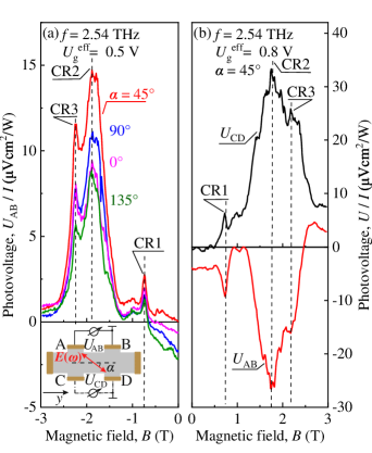
Upon excitation of the sample with linearly polarized radiation with THz and sweeping the magnetic field we observed three pronounced resonances at fields labeled in Fig. 2 as CR1, CR2, and CR3. The data were detected between contacts located on the long Hall bar edges. Figures 2(a) and (b) show two central observations: (i) the appearance of the resonances in the magnetic field dependence of the photoresponse and (ii) the signal polarity is consistently opposite for opposite edges. In addition, Fig. 2(a) reveals that the amplitude of the resonance depends on the orientation of the radiation electric field vector with respect to the edges. Positions of the resonances, their dependencies on the gate voltage, polarization, radiation frequency, and other parameters will be described and discussed later. First, we focus on the relative sign of the signals measured for the contact pairs AB and CD. The experimental setup is shown in the inset of Fig. 2(a). From the electric circuits used is seen that the positive signal picked up from the contacts CD and the negative one detected for the contacts AB indicate that the photocurrents along opposite edges flow in the opposite directions. This is only possible if the signal is generated at the edges and not in the graphene bulk (in the latter case current projections on the lines AB and CD would have the same direction). This observation, together with the fact that the signals for opposite edges have almost the same magnitudes, indicates that the signal stems from the photocurrent flowing along the sample edges. The edge contribution can be obtained by subtracting the signals measured at the opposite sides, .
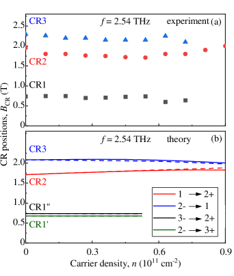
Figure 3(a) demonstrates that the resonance edge photosignals have opposite signs for opposite polarities of , i.e. is odd in magnetic field. Varying the Fermi level position by changing the back gate voltage we observed that at moderate gate voltages CR1 and CR3 become less pronounced in comparison to CR2, see Fig. 3(b), and at even higher gate voltage these vanish. Positions of CR1, CR2, and CR3 as a function of the carrier density are plotted in Fig. 4(a). When the carrier density changes from to cm-2, only weak shifts of the resonances are observed.
Changing the radiation frequency from 2.54 to 0.69 THz results in the shift of CR2 and CR1 by about 3.7 times, which proves that the resonance positions scale linearly with , see Fig. 3(c). Note that for THz the resonance CR3 vanish. As we will show below the resonance positions together with their behaviour upon variation of the carrier density and radiation frequency demonstrate that the resonances are caused by the cyclotron resonances involving transitions between valence and conduction bands (CR1 and CR3) and within the conduction band (CR2).
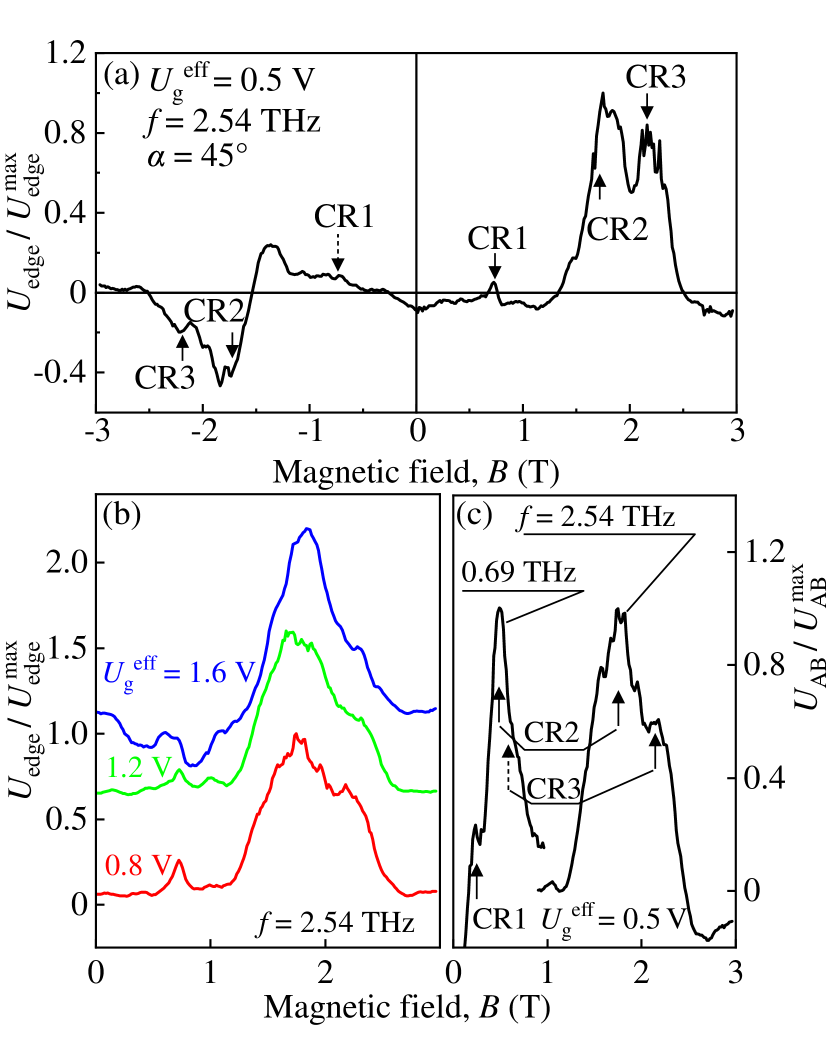
The data discussed so far were obtained at low gate voltages (below 1.5 V) and, consequently, low carrier densities (). At higher carrier densities the analysis of the CR-induced photocurrent becomes more complicated, because the resonances are superimposed by the SdH-related oscillations in the photocurrent, see Fig. 5. The carrier densities calculated from the period of the oscillations of the photocurrent are the same as those calculated from the corresponding gate voltages. The figure shows, however, that the oscillating signal is strongly enhanced at magnetic fields of about 1.8 to 2.6 T. The observed enhancement can be satisfactory described assuming a single resonance with a position depending on the carrier density. Our analysis below demonstrates that this behaviour is well described by the density dependence of the cyclotron resonance caused by optical transitions within the conduction band. Note that these results provide an additional evidence for the absence of resonances CR1 and CR3 at high carrier density.
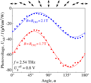
As addressed above, the magnitudes of the CR-induced photocurrents change upon rotation of the radiation electric field vector with respect to the edges, see Fig. 2(a). The dependence of the signal on the azimuth angle can be well fitted by Candussio et al. (2020); Plank et al. (2018)
| (1) |
see Fig. 6 for contacts AB (upper edge). Here and are the amplitudes of the polarization dependent and independent contributions, respectively. Note that for the CR-induced signals the phase shift is almost zero. Furthermore, while the signal strength varies with the azimuth angle, the sign of the resonance response remains the same and is defined by the magnetic field polarity only.

IV Identification of cyclotron resonances
To identify optical transitions responsible for the observed cyclotron resonances we obtain the energy dispersion of carriers in bilayer graphene as a function of the magnetic field and consider the corresponding selection rules. Bilayer graphene has a unit cell with 4 carbon atoms, , where of the top layer lies above of the bottom layer. The dispersion is described with a Slonczewski-Weiss-McClure tight-binding model parameterized by Slonczewski and Weiss (1958); McClure (1957); Dresselhaus and Dresselhaus (2002) parameters (minus hoppings), ( hopping), (minus hopping), ( and hoppings), (sublattice energy difference and ) and top-bottom asymmetry parameter that is induced by a vertical electric displacement field since the field of the bottom gate is not fully screened by the bottom graphene layer. Note that this parameter defines the gap. The resulting 4-band tight-binding model has been used to compute numerically the spectrum of Landau levels and the parameter has been found from self-consistent Hartree approximation that is formulated as McCann and Fal’ko (2006); McCann and Koshino (2013); Slizovskiy et al. (2019)
where is the interlayer separation, accounts for electric polarizability of carbon orbitals in graphene and (constrained as ) are the density of electrons at graphene layers that can be found from the wave functions of occupied Landau levels with phenomenological broadening.
To clarify the labeling of the Landau levels and give qualitative understanding of the results we note that the 4-band model can be reduced to an effective 2-band model with Hamiltonian McCann and Koshino (2013); McCann and Fal’ko (2006); Mucha-Kruczyński et al. (2010)
| (4) | |||||
| (9) | |||||
| (12) | |||||
| (17) |
where , , , is a lattice constant of graphene and denotes the valleys. We note that is responsible for electron-hole asymmetry of the spectrum (with holes being slightly more massive), is a trigonal warping term and is a top-bottom asymmetry term that inevitably arizes in single-gated devices and is responsible for the gap between valence and conduction bands.
In the standard basis of magnetic eigenstates , where are harmonic oscillator eigenstates and , the operators act as lowering operators at the valley and as raising operators in the opposite valley. This allows us to find the spectrum of Landau levels analytically once we neglect the trigonal warping term. In the valley the spectrum is
| (19) | |||||
| (22) | |||||
| (25) |
This clarifies the labeling of LLs as , shown in Fig. 7 ( corresponds to Landau levels in conduction/valence band). To calculate the LL spectrum for the valley must be substituted by .
The allowed optical transitions are obtained from the selection rules following Ref. [Abergel and Fal’ko, 2007]. For the circularly polarized radiation the allowed transitions are
when is parallel to the direction of light angular momentum ( in Fig. 7) or
when is anti-parallel to the direction of light angular momentum ( in Fig. 7). The energy of and transitions are slightly valley-split when , while for other transitions the valley splitting is negligibly small. The transitions at correspond to classical CR transitions for holes, transitions are classical CR for electrons, while the rest are the quantum inter-band transitions. Note that level does not participate in radiation emission/absorption in case of a small asymmetry parameter, see Ref. Abergel and Fal’ko (2007). The selection rules need to be combined with the conditions that the initial (final) states are, at least partially, filled (empty). At low electron density and for a frequency of THz these yield four resonances labeled CR1′, CR1′′, CR2, and CR3 in Fig. 7. The calculated positions correspond well to those detected in experiment, see, e.g., Fig. 2. Because CRs are excited by linearly polarized radiation the resonances in Fig. 7 at positive (negative) magnetic field appear also for negative (positive) . Note that in experiment the transitions CR1′ and CR1′′ are not resolved because they have very close positions. We also note that the difference in the CR2 and CR3 peak positions is due to electron-hole asymmetry of the spectrum ( term in Hamiltonian), which results in a greater mass of holes. With the carrier density increasing the final states for the inter-band transitions in CR3, CR1′, and CR1′′ become occupied and these resonances vanish. This is indeed observed in the experiment, see Fig. 4. The occupation of the final states is also the reason of disappearance of the CR3 resonance at substantial frequency reduction, see Fig. 3(c).
At high densities, the classical regime applies and the distance between the neighboring Landau levels and for , determining the position of CR, is given by
where we have to keep the term containing since the latter grows almost linearly with increasing doping and hence is important even at large . The values of resonance magnetic field are calculated using Eq. (25) at low carrier density and Eq. (IV) at high carrier density corresponding to the semiclassical regime. The calculated values of were then used to fit the data in Fig. 5. The growth of with gate voltage explains the reduction of LL separation, and, consequently, the growth of with increasing electron density.
Below we show that at cyclotron resonance the edge current flows within a strip with the width equal to the cyclotron diameter (, where is the carrier velocity at the Fermi level). This value is around tens of nanometers and is already smaller than the free path length at experimental conditions. Therefore, at CR we probe a few tens of nm wide region near the edge. For low gate voltages, the doping near the edge is the same as in the bulk, so the CR position is determined by the bulk doping level. In general, at higher gate voltages (as used in Fig. 5), the doping may become notably inhomogeneous near the edge of the graphene–back gate capacitor at the scale nm, where nm is the distance to the bottom gate Silvestrov and Efetov (2008); Slizovskiy and Fal’ko (2018) and is the dielectric constant of SiO2 dielectric. This effect may lead to broadening of the edge current region and to deviations of the CR position from that predicted from the bulk doping. However, carrier densities obtained from the period of the photocurrent oscillations, Fig. 5, coincide with that calculated from the corresponding gate voltages.
Our analysis below demonstrates that the resonant behaviour of the observed edge photocurrents upon variation of the magnetic field follows the semiclassical shape of the CR in the absorbance, given by
| (27) |
Apart from the conventional transport width of the CR given by the momentum relaxation rate , here we include an additional electrodynamic contribution, , where is the cyclotron mass, which accounts for a significant reflection of the radiation in the vicinity of CR in high density samples Fal’ko and Khmel’nitskii (1989); Mikhailov (2004); Herrmann et al. (2016). The radiative decay parameters calculated for different are summarized in Tab. 1. The curves calculated after the right-hand side of Eq. (27) are shown by dashed lines in Fig. 5 demonstrating a good agreement with the experimental data. In these plots we used the cyclotron electron mass obtained from the calculated CR positions.
The values of in the low-density regime were calculated after Eq. (25) for the transitions between the lowest Landau levels, see Fig. 5(a) and resonances , , and . In the high density regime was obtained from Eq. (IV) for the intra-band transitions between the neighboring Landau levels in the conduction band, see in Figs. 5(b), (c), and (d).
At low electron density, see Fig. 5(a), the halfwidth of the CR detected in the edge vicinity is substantially larger than that expected for the radiative decay , being for V equal to 0.06 , see Tab. 1. Therefore, the width of the resonance, in this case, is determined by the momentum relaxation time of the electrons in the edge channels 111Note that the values of the order of ps corresponds well to those reported in Ref. Cobaleda et al. (2014) obtained for the suspended bilayer graphene with the carrier mobility about cm2/Vs and the mass .. The value of ps, however, is half as much as expected for our samples with the carrier mobility of cm2/Vs and the cyclotron mass of (see Tab. 1). We attribute the difference in the momentum relaxation times extracted from the transport measurements and from the CR data to the fact that the value of extracted from the edge photocurrent measurements may be shorter than that obtained in bulk magnetotransport experiments. At higher densities, the radiative decay rate increases, see Tab. 1, and becomes higher than the reciprocal momentum relaxation times. Thus, the width of the resonance detected at high carrier densities is determined by the radiative decay and this value cannot be used to extract the momentum relaxation time at the edges.
While the overall agreement obtained without fitting parameters is encouraging, we should mention that the used semiclassical description becomes less accurate at low densities corresponding to transitions between low-lying Landau levels. Here the electrodynamic effects are negligible, but Landau quantization effect should be taken into account Dmitriev et al. (2012). In Fig. 5, one clearly distinguishes four CR lines corresponding to different intra-band ( and ) and inter-band ( and ) transitions between distinct Landau levels.
| [V] | [] | [T] | ||
|---|---|---|---|---|
| 0.5 | 0.23 | 0.020 | 0.06 | |
| 9.5 | 4.37 | 0.023 | 1.00 | |
| 15 | 6.90 | 0.026 | 1.40 | |
| 20 | 9.20 | 0.029 | 1.70 |

V Edge photocurrent at cyclotron resonance in classical regime
In this section we discuss the model describing cyclotron resonances in the dc edge current. Edge photocurrent induced by terahertz radiation at zero and low magnetic fields far from the cyclotron resonance conditions was studied in bilayer graphene in our previous work Candussio et al. (2020). It was shown that the dc edge current is induced by the high-frequency electric field of the incident THz radiation due to the breaking of the parity symmetry at the edge. This phenomenon can be viewed as a dc conversion of the bulk ac electric current at the edge. Two possible microscopic mechanisms of such an ac-dc conversion were discussed. The first one is based on the alignment of the free carrier momenta by the high-frequency electric field and subsequent scattering of the carriers at the edge. The second one is related to the dynamic charge accumulation near the edge and synchronized charge motion along the edge. In line with Ref. Candussio et al. (2020) the dc edge current observed in the present work at low magnetic field behaves as , where is the phase shift induced by the applied magnetic field.
In the current work we present the theory of the edge photocurrent at high magnetic fields satisfying the cyclotron resonance conditions, when the driving frequency is close to the cyclotron frequency . As seen in Figs. 2 and 6, the polarization and magnetic field dependencies of the edge photovoltage in the CR regime differ significantly from those at zero or low magnetic field addressed above. The sign of the voltage no longer depends on the orientation of the electric field with respect to the edge, see Ref. Candussio et al. (2020), but is defined by the direction of magnetic field.
Such a behaviour can be explained by the following model, see Fig. 8. Here, we discuss the model for positively charged holes, however its generalization to electrons is straightforward. At the holes in the 2D layer move along cyclotron orbits. When the frequency of the driving electric field coincides with the cyclotron frequency, the motion of holes becomes synchronized. The integral velocity of holes in the bulk of the 2D plane rotates following the rotating electric field of the incident wave. The oscillating electric field also leads to periodic accumulation and depletion of holes at the edge, however, the hole density oscillates with a retardation as compared to electric field. This fact follows from the continuity equation , where is the hole density and is the hole flux normal to the edge. One may say, that the oscillations of the hole density at the edge are driven by the electric field , which is shifted by a quarter of period in time with respect to . Due to holes accumulation and depletion, the integral hole velocity near the edge differs from . In the first half-period of the electric-field oscillations, when , the retarded field points towards the edge leading to accumulation of holes at the edge and, consequently, to . At the second half-period, when , points towards the bulk leading to depletion of holes at the edge, and during that time interval . Consequently in the vicinity of the edges such asymmetric oscillations of result in a net dc current flowing along the edge. This current is formed near the edge within a strip of the width equal to the diameter of the cyclotron orbit . As seen in Fig. 8, the direction of this current is determined by the direction of the cyclotron motion, and hence, by the sign of the magnetic field. The model suggests, that the increase of the edge current at the cyclotron resonance is related to the increase of and due to resonant absorption.
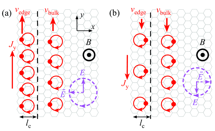
The discussed mechanism describes the formation of the edge current at classical magnetic fields, when , where is the Fermi energy. It is valid for intra-band absorption at high carrier densities, see the observed resonance in Figs. 5 (b-d). Resonances CR1 and CR3 are caused by inter-band transitions between valence and conduction band Landau levels and formation of the edge current in that case should be considered separately Plank et al. (2018).
For microscopic description of the edge photocurrent we apply the Boltzmann approach, which is valid for the classical range of the driving field frequency , corresponding to intra-band absorption of the incident radiation. We consider a semi-infinite 2D gas of charge carriers occupying half-space. To derive the edge photocurrent we follow the procedure of Ref. Candussio et al. (2020). We further analyse the spectral and polarization dependencies of the calculated current in the vicinity of the cyclotron resonance.
The distribution function of the charge carriers (electrons or holes) is found from the Boltzmann kinetic equation
| (28) |
where is the total electric field in the sample consisting of the ac field of the incident wave and the local screening field due to redistribution of charge, is the magnetic field, and are the carrier momentum and velocity, respectively, is the distribution function averaged over directions of , is the relaxation time, is the carrier electric charge and is the effective mass. In what follows we assume that is independent of carrier energy. The kinetic equation should be supplemented with a boundary condition at . Here we consider the specular reflection of carriers at the sample edge implying that the distribution function satisfies .
Equation (28) is solved by expanding the distribution function in a series over the electric field as , where is the equilibrium distribution function, , and Karch et al. (2011). The density of the dc edge current is determined by the time-independent correction and reads
| (29) |
where the factor 4 accounts for the spin and valley degeneracy. Using Eq. (28) one can present as Candussio et al. (2020)
| (30) |
To calculate using Eq. (30) one needs to find and from Eq. (28), which can be done numerically. However, as shown in Ref. Candussio et al. (2020), the total current flowing along the edge is found analytically and can be expressed in terms of the conductivity tensor. Substituting the expression for the conductivity tensor in Eq. (13) of Ref. Candussio et al. (2020) and setting we obtain
| (31) |
where
| (32) | |||||
Here is the conductivity of 2D electron (or hole) gas at zero magnetic field, and is the cyclotron frequency. As follows from Eq. (32), the dc edge current in presence of a magnetic field is induced by linearly polarized radiation with nonzero terms or , circularly polarized radiation with nonzero , and also unpolarized radiation.
Let us now consider the behaviour of the edge photocurrent (31) in the vicinity of the cyclotron resonance, i.e. in the frequency range and . For linearly polarized radiation the edge current is determined by the first, third, and fourth terms in Eq. (31). The cyclotron resonance occurs for both directions of magnetic field at , where . Near the resonance the edge current given by Eqs. (31) and (32) is simplified to
| (33) |
Here is the electric field angle with respect to the edge,
| (34) |
is the absorbance of the 2D layer in the vicinity of cyclotron resonance and far from the edge for non-polarized radiation, is the intensity of the radiation, and is the refractive index of the dielectric medium surrounding bilayer graphene. The phase shift is determined from
| (35) |
The sign, magnitude, and polarization dependence of the edge dc current given by Eqs. (33) and (34) are in agreement with experimental observations, shown in Figs. 2, 3, and 6. Equations (33) and (34) show that the edge dc current at cyclotron resonance is proportional to the absorbed energy. Therefore, an increase of the edge current magnitude at cyclotron resonance is due to the increase of absorption. The direction of the edge current is determined by the direction of magnetic field in agreement with experimental data in Figs. 2 and 3, which show the change of the photovoltage sign for opposite directions of the magnetic field. Interestingly, the direction of the dc current is the same for electrons and holes. These characteristic features are similar to those observed for the edge photocurrent at strong magnetic field under conditions of the quantum Hall effect Plank et al. (2018).
As follows from Eq. (33), the edge current induced by linearly polarized radiation consists of a polarization-independent contribution and a contribution that is sensitive to the orientation of the electric field. The second contribution is less than the first one. The phase shift , given by Eq. (35), vanishes at the resonance so that the polarization dependent part of behaves as . Weak dependence of the edge current on polarization and behaviour are in line with experimental observations shown in Fig. 6. Far from resonance, when , we have , so that the polarization dependent part of behaves as .
For circularly polarized radiation the edge photocurrent is determined by the first two terms in Eq. (31). The cyclotron resonance occurs for a particular direction of the magnetic field at , where , for right (left)-hand circularly polarized radiation. Near the resonance Eq. (31) yields
| (36) |
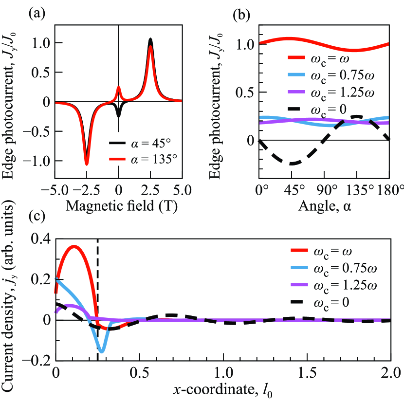
Figure 9(a) shows the edge photocurrent calculated after Eqs. (31) and (32) as a function of the magnetic field. The calculations were done for two linear polarizations , corresponding to and . Parameters used in calculations are the same as in calculations of the dashed curve in Fig. 5(c), see V in Tab. 1. Sharp cyclotron resonances in the edge current occur at T with magnitude, which is almost independent of the polarization, and sign, which is determined by the direction of magnetic field. These results are in good agreement with experimental observations, see Figs. 2, 3, and 5. By contrast, the directions of the dc current at is opposite for and , see Ref. Candussio et al. (2020). The dependence of on is shown in Fig. 9(b) for different values of corresponding to the resonances CR2 and CR3. Note that the dependencies are presented for low densities corresponding to CRs in the quantum mechanical limit, because at higher densities the SdH-like oscillations make it difficult to extract the CR’s amplitude and, consequently, do not allow us to analyze its polarization dependence. Nevertheless, it is clear that the polarization dependence of the edge photocurrent at CR is indeed very weak. Its polarization dependent part follows dependence, whereas out of the resonance the polarization dependence of changes to (see Fig. 9). This is in line with Eq. (33) and describes the experimental results, see Fig. 6. The distribution of the edge photocurrent density , calculated after Eq. (30) with found numerically from Eq. (28), is shown in Fig. 9(c). The results are obtained for circularly polarized radiation when the first term is Eq. (30) vanishes. It is seen that at the dc current flows mainly in the strip of the width equal to the cyclotron diameter , which at these conditions is much less than the mean free path . By contrast, at zero magnetic field the current is distributed over a much larger length .
VI Summary
We reported on the observation and study of cyclotron resonance induced edge photocurrents in high mobility hBN encapsulated bilayer graphene. The cyclotron masses, momentum relaxation time, and carrier densities determined from the position and shape of CR together with the analysis of -periodic magnetooscillations demonstrate that in studied samples and for the investigated carrier density range these parameters do not distinguish from those of the material bulk. Experimental findings for high carrier densities corresponding to the semiclassical regime are explained within the microscopic model based on the Boltzmann kinetic equation. Theoretical model describing the edge photocurrent at low carrier density, when the cyclotron resonance emerges due to inter-band or intra-band transitions between the lowest Landau levels, is a future task.
VII Appendix 1
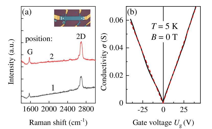
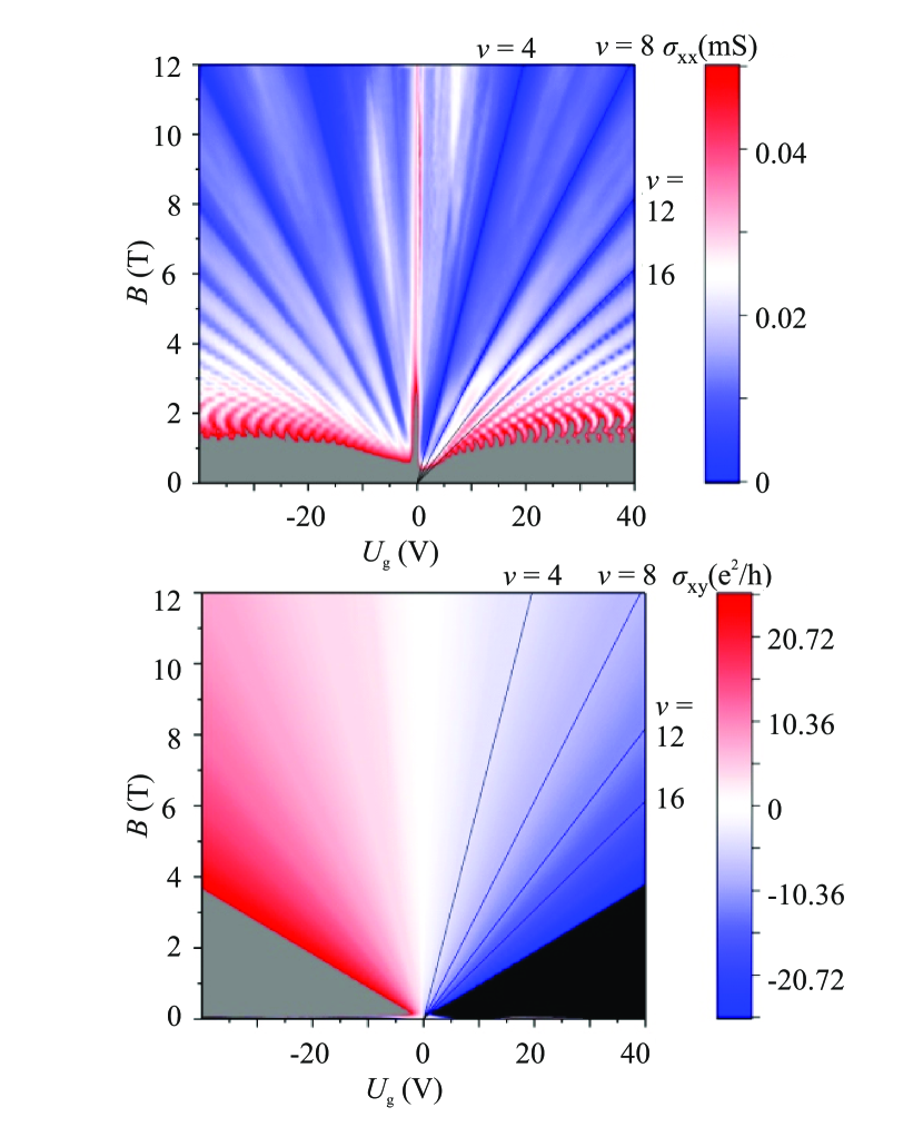
Figures 10 (a),(b), and 11 show the Raman spectra, dependence of the conductivity on the gate voltage, and magnetotransport results, respectively.
The micro-Raman scattering data obtained for two laser spot positions, see Fig. 10 (a) ensure that the fabricated sample is bilayer graphene. The transport results are used to determine the mobility which is on the hole side cm2/Vs and on the electron side cm2/Vs. Note that the Drude charge carrier mobility approach cannot be used for the region close to CNP. From low temperature magnetotransport we can unambiguously confirm that our sample is the bilayer graphene. Namely, the longitudinal conductivity map shows strong cyclotron gaps (seen as dark blue lines in the top panel of Fig. 11) at filling factors , consistent with the Landau level spectrum of bilayer graphene Novoselov et al. (2006); McCann and Fal’ko (2006).
VIII Acknowledgments
We thank S.A. Tarasenko, I.A. Dmitriev, and H. Plank for helpful discussions. The support from the Deutsche Forschungsgemeinschaft (DFG, German Research Foundation) – Project SPP 2244 (GA501/17-1), the Elite Network of Bavaria (K-NW-2013-247), and the Volkswagen Stiftung Program (97738) is gratefully acknowledged. S.D.G. acknowledges support of the Foundation for Polish Science (IRA Program, grant MAB/2018/9, CENTERA). M. V. D. acknowledges financial support from the Russian Science Foundation (Project No. 19-72-00029). VF and SS acknowledges support from European Graphene Flagship Project (Core3), ERC Synergy Grant Hetero2D, EPSRC grant EP/V007033/1. AM acknowledges support of the EPSRC Early Career Fellowship (EP/N007131/1)and the European Research Council (ERC) under the European Union’s Horizon 2020 research and innovation programme (grant agreement No. 865590).
References
- v. Klitzing et al. (1980) K. v. Klitzing, G. Dorda, and M. Pepper, Phys. Rev. Lett. 45, 494 (1980).
- Halperin (1982) B. I. Halperin, Phys. Rev. B 25, 2185 (1982).
- Sarma and Pinczuk (1997) S. D. Sarma and A. Pinczuk, Perspectives in Quantum Hall Effects (John Wiley and Sons, New York, 1997).
- Novoselov et al. (2006) K. S. Novoselov, E. McCann, S. V. Morozov, V. I. Fal’ko, M. I. Katsnelson, U. Zeitler, D. Jiang, F. Schedin, and A. K. Geim, Nat. Phys. 2, 177 (2006).
- Neto et al. (2009) A. H. C. Neto, F. Guinea, N. M. R. Peres, K. S. Novoselov, and A. K. Geim, Rev. Mod. Phys. 81, 109 (2009).
- Murakami et al. (2004) S. Murakami, N. Nagaosa, and S.-C. Zhang, Phys. Rev. Lett. 93, 156804 (2004).
- Kane and Mele (2005) C. L. Kane and E. J. Mele, Phys. Rev. Lett. 95, 146802 (2005).
- Bernevig and Zhang (2006) B. A. Bernevig and S.-C. Zhang, Phys. Rev. Lett. 96, 106802 (2006).
- König et al. (2007) M. König, S. Wiedmann, C. Brune, A. Roth, H. Buhmann, L. W. Molenkamp, X.-L. Qi, and S.-C. Zhang, Science 318, 766 (2007).
- Hasan and Kane (2010) M. Z. Hasan and C. L. Kane, Rev. Mod. Phys. 82, 3045 (2010).
- Qi and Zhang (2011) X.-L. Qi and S.-C. Zhang, Rev. Mod. Phys. 83, 1057 (2011).
- Martin et al. (2008) I. Martin, Y. M. Blanter, and A. F. Morpurgo, Phys. Rev. Lett. 100, 036804 (2008).
- Yao et al. (2009) W. Yao, S. A. Yang, and Q. Niu, Phys. Rev. Lett. 102, 096801 (2009).
- Zhang et al. (2011) F. Zhang, J. Jung, G. A. Fiete, Q. Niu, and A. H. MacDonald, Phys. Rev. Lett. 106, 156801 (2011).
- Jung et al. (2011) J. Jung, F. Zhang, Z. Qiao, and A. H. MacDonald, Phys. Rev. B 84, 075418 (2011).
- Vaezi et al. (2013) A. Vaezi, Y. Liang, D. H. Ngai, L. Yang, and E.-A. Kim, Phys. Rev. X 3, 021018 (2013).
- Sanchez-Yamagishi et al. (2016) J. D. Sanchez-Yamagishi, J. Y. Luo, A. F. Young, B. M. Hunt, K. Watanabe, T. Taniguchi, R. C. Ashoori, and P. Jarillo-Herrero, Nat. Nanotechnol. 12, 118 (2016).
- Niimi et al. (2006) Y. Niimi, T. Matsui, H. Kambara, K. Tagami, M. Tsukada, and H. Fukuyama, Phys. Rev. B 73, 085421 (2006).
- Ritter and Lyding (2009) K. A. Ritter and J. W. Lyding, Nat. Mater. 8, 235 (2009).
- Yin et al. (2016) L.-J. Yin, H. Jiang, J.-B. Qiao, and L. He, Nat. Commun. 7, 11760 (2016).
- Casiraghi et al. (2009) C. Casiraghi, A. Hartschuh, H. Qian, S. Piscanec, C. Georgi, A. Fasoli, K. S. Novoselov, D. M. Basko, and A. C. Ferrari, Nano Lett. 9, 1433 (2009).
- Heydrich et al. (2010) S. Heydrich, M. Hirmer, C. Preis, T. Korn, J. Eroms, D. Weiss, and C. Schüller, Appl. Phys. Lett. 97, 043113 (2010).
- Begliarbekov et al. (2010) M. Begliarbekov, O. Sul, S. Kalliakos, E.-H. Yang, and S. Strauf, Appl. Phys. Lett. 97, 031908 (2010).
- Nowack et al. (2013) K. C. Nowack, E. M. Spanton, M. Baenninger, M. König, J. R. Kirtley, B. Kalisky, C. Ames, P. Leubner, C. Brüne, H. Buhmann, L. W. Molenkamp, D. Goldhaber-Gordon, and K. A. Moler, Nat. Mater. 12, 787 (2013).
- Marguerite et al. (2019) A. Marguerite, J. Birkbeck, A. Aharon-Steinberg, D. Halbertal, K. Bagani, I. Marcus, Y. Myasoedov, A. K. Geim, D. J. Perello, and E. Zeldov, Nature 575, 628 (2019).
- Slota et al. (2018) M. Slota, A. Keerthi, W. K. Myers, E. Tretyakov, M. Baumgarten, A. Ardavan, H. Sadeghi, C. J. Lambert, A. Narita, K. Müllen, and L. Bogani, Nature 557, 691 (2018).
- Liu et al. (2009) Z. Liu, K. Suenaga, P. J. F. Harris, and S. Iijima, Phys. Rev. Lett. 102, 015501 (2009).
- Ju et al. (2015) L. Ju, Z. Shi, N. Nair, Y. Lv, C. Jin, J. Velasco, C. Ojeda-Aristizabal, H. A. Bechtel, M. C. Martin, A. Zettl, J. Analytis, and F. Wang, Nature 520, 650 (2015).
- Fei et al. (2015) Z. Fei, M. D. Goldflam, J.-S. Wu, S. Dai, M. Wagner, A. S. McLeod, M. K. Liu, K. W. Post, S. Zhu, G. C. A. M. Janssen, M. M. Fogler, and D. N. Basov, Nano Lett. 15, 8271 (2015).
- Jiang et al. (2016) L. Jiang, Z. Shi, B. Zeng, S. Wang, J.-H. Kang, T. Joshi, C. Jin, L. Ju, J. Kim, T. Lyu, Y.-R. Shen, M. Crommie, H.-J. Gao, and F. Wang, Nat. Mater. 15, 840 (2016).
- Nikitin et al. (2016) A. Y. Nikitin, P. Alonso-González, S. Vélez, S. Mastel, A. Centeno, A. Pesquera, A. Zurutuza, F. Casanova, L. E. Hueso, F. H. L. Koppens, and R. Hillenbrand, Nat. Photonics 10, 239 (2016).
- Li et al. (2016) P. Li, I. Dolado, F. J. Alfaro-Mozaz, A. Y. Nikitin, F. Casanova, L. E. Hueso, S. Vélez, and R. Hillenbrand, Nano Lett. 17, 228 (2016).
- Karch et al. (2011) J. Karch, C. Drexler, P. Olbrich, M. Fehrenbacher, M. Hirmer, M. M. Glazov, S. A. Tarasenko, E. L. Ivchenko, B. Birkner, J. Eroms, D. Weiss, R. Yakimova, S. Lara-Avila, S. Kubatkin, M. Ostler, T. Seyller, and S. D. Ganichev, Phys. Rev. Lett. 107, 276601 (2011).
- Glazov and Ganichev (2014) M. Glazov and S. Ganichev, Phys. Rep. 535, 101 (2014).
- Dantscher et al. (2017) K.-M. Dantscher, D. A. Kozlov, M. T. Scherr, S. Gebert, J. Bärenfänger, M. V. Durnev, S. A. Tarasenko, V. V. Bel’kov, N. N. Mikhailov, S. A. Dvoretsky, Z. D. Kvon, J. Ziegler, D. Weiss, and S. D. Ganichev, Phys. Rev. B 95, 201103(R) (2017).
- Luo and Li (2017) M. Luo and Z. Li, Phys. Rev. B 96, 165424 (2017).
- Ganichev et al. (2017) S. D. Ganichev, D. Weiss, and J. Eroms, Ann. Phys. 529, 1600406 (2017).
- Xu et al. (2018) S.-Y. Xu, Q. Ma, H. Shen, V. Fatemi, S. Wu, T.-R. Chang, G. Chang, A. M. M. Valdivia, C.-K. Chan, Q. D. Gibson, J. Zhou, Z. Liu, K. Watanabe, T. Taniguchi, H. Lin, R. J. Cava, L. Fu, N. Gedik, and P. Jarillo-Herrero, Nat. Phys. 14, 900 (2018).
- Plank et al. (2018) H. Plank, M. V. Durnev, S. Candussio, J. Pernul, K.-M. Dantscher, E. Mönch, A. Sandner, J. Eroms, D. Weiss, V. V. Bel’kov, S. A. Tarasenko, and S. D. Ganichev, 2D Mater. 6, 011002 (2018).
- Durnev and Tarasenko (2019) M. V. Durnev and S. A. Tarasenko, Ann. Phys. 531, 1800418 (2019).
- Candussio et al. (2020) S. Candussio, M. V. Durnev, S. A. Tarasenko, J. Yin, J. Keil, Y. Yang, S.-K. Son, A. Mishchenko, H. Plank, V. V. Bel’kov, S. Slizovskiy, V. Fal’ko, and S. D. Ganichev, Phys. Rev. B 102, 045406 (2020).
- Otteneder et al. (2020) M. Otteneder, S. Hubmann, X. Lu, D. A. Kozlov, L. E. Golub, K. Watanabe, T. Taniguchi, D. K. Efetov, and S. D. Ganichev, Nano Lett. 20, 7152 (2020).
- Vicarelli et al. (2012) L. Vicarelli, M. S. Vitiello, D. Coquillat, A. Lombardo, A. C. Ferrari, W. Knap, M. Polini, V. Pellegrini, and A. Tredicucci, Nat. Mater. 11, 865 (2012).
- Freitag et al. (2013) M. Freitag, T. Low, and P. Avouris, Nano Lett. 13, 1644 (2013).
- Koppens et al. (2014) F. H. L. Koppens, T. Mueller, P. Avouris, A. C. Ferrari, M. S. Vitiello, and M. Polini, Nat. Nanotechnol. 9, 780 (2014).
- Olbrich et al. (2016) P. Olbrich, J. Kamann, M. König, J. Munzert, L. Tutsch, J. Eroms, D. Weiss, M.-H. Liu, L. E. Golub, E. L. Ivchenko, V. V. Popov, D. V. Fateev, K. V. Mashinsky, F. Fromm, T. Seyller, and S. D. Ganichev, Phys. Rev. B 93, 235439 (2016).
- Auton et al. (2016) G. Auton, J. Zhang, R. K. Kumar, H. Wang, X. Zhang, Q. Wang, E. Hill, and A. Song, Nat. Commun. 7, 11670 (2016).
- Auton et al. (2017) G. Auton, D. B. But, J. Zhang, E. Hill, D. Coquillat, C. Consejo, P. Nouvel, W. Knap, L. Varani, F. Teppe, J. Torres, and A. Song, Nano Lett. 17, 7015 (2017).
- Bandurin et al. (2018) D. A. Bandurin, D. Svintsov, I. Gayduchenko, S. G. Xu, A. Principi, M. Moskotin, I. Tretyakov, D. Yagodkin, S. Zhukov, T. Taniguchi, K. Watanabe, I. V. Grigorieva, M. Polini, G. N. Goltsman, A. K. Geim, and G. Fedorov, Nat. Commun. 9, 5392 (2018).
- Castilla et al. (2019) S. Castilla, B. Terrés, M. Autore, L. Viti, J. Li, A. Y. Nikitin, I. Vangelidis, K. Watanabe, T. Taniguchi, E. Lidorikis, M. S. Vitiello, R. Hillenbrand, K.-J. Tielrooij, and F. H. Koppens, Nano Lett. 19, 2765 (2019).
- Delgado-Notario et al. (2020) J. A. Delgado-Notario, V. Clericò, E. Diez, J. E. Velázquez-Pérez, T. Taniguchi, K. Watanabe, T. Otsuji, and Y. M. Meziani, APL Photonics 5, 066102 (2020).
- Lee et al. (2011) J. Lee, K. S. Novoselov, and H. S. Shin, ACS Nano 5, 608 (2011).
- Ganichev et al. (1982) S. D. Ganichev, S. A. Emel’yanov, and I. D. Yaroshetskii, JETP Lett. 35, 368 (1982).
- Olbrich et al. (2013) P. Olbrich, C. Zoth, P. Vierling, K.-M. Dantscher, G. V. Budkin, S. A. Tarasenko, V. V. Bel’kov, D. A. Kozlov, Z. D. Kvon, N. N. Mikhailov, S. A. Dvoretsky, and S. D. Ganichev, Phys. Rev. B 87, 235439 (2013).
- Plank et al. (2016) H. Plank, L. E. Golub, S. Bauer, V. V. Bel’kov, T. Herrmann, P. Olbrich, M. Eschbach, L. Plucinski, C. M. Schneider, J. Kampmeier, M. Lanius, G. Mussler, D. Grützmacher, and S. D. Ganichev, Phys. Rev. B 93, 125434 (2016).
- Slonczewski and Weiss (1958) J. C. Slonczewski and P. R. Weiss, Phys. Rev. 109, 272 (1958).
- McClure (1957) J. W. McClure, Phys. Rev. 108, 612 (1957).
- Dresselhaus and Dresselhaus (2002) M. S. Dresselhaus and G. Dresselhaus, Adv. Phys. 51, 1 (2002).
- McCann and Fal’ko (2006) E. McCann and V. I. Fal’ko, Phys. Rev. Lett. 96, 086805 (2006).
- McCann and Koshino (2013) E. McCann and M. Koshino, Rep. Prog. Phys. 76, 056503 (2013).
- Slizovskiy et al. (2019) S. Slizovskiy, A. Garcia-Ruiz, N. Drummond, and V. I. Falko, arXiv:1912.10067 (2019).
- Mucha-Kruczyński et al. (2010) M. Mucha-Kruczyński, E. McCann, and V. I. Fal’ko, Semicond. Sci. Technol. 25, 033001 (2010).
- Abergel and Fal’ko (2007) D. S. L. Abergel and V. I. Fal’ko, Phys. Rev. B 75, 155430 (2007).
- Silvestrov and Efetov (2008) P. G. Silvestrov and K. B. Efetov, Phys. Rev. B 77, 155436 (2008).
- Slizovskiy and Fal’ko (2018) S. Slizovskiy and V. I. Fal’ko, Phys. Rev. B 97, 075404 (2018).
- Fal’ko and Khmel’nitskii (1989) V. I. Fal’ko and D. E. Khmel’nitskii, Sov. Phys. JETP 68, 1150 (1989).
- Mikhailov (2004) S. A. Mikhailov, Phys. Rev. B 70, 165311 (2004).
- Herrmann et al. (2016) T. Herrmann, I. A. Dmitriev, D. A. Kozlov, M. Schneider, B. Jentzsch, Z. D. Kvon, P. Olbrich, V. V. Bel’kov, A. Bayer, D. Schuh, D. Bougeard, T. Kuczmik, M. Oltscher, D. Weiss, and S. D. Ganichev, Phys. Rev. B 94, 081301 (2016).
- Note (1) Note that the values of the order of ps corresponds well to those reported in Ref. Cobaleda et al. (2014) obtained for the suspended bilayer graphene with the carrier mobility about cm2/Vs and the mass .
- Dmitriev et al. (2012) I. A. Dmitriev, A. D. Mirlin, D. G. Polyakov, and M. A. Zudov, Rev. Mod. Phys. 84, 1709 (2012).
- Cobaleda et al. (2014) C. Cobaleda, S. Pezzini, E. Diez, and V. Bellani, Phys. Rev. B 89, 121404(R) (2014).