Superconducting circuits without inductors based on bistable Josephson junctions
Abstract
Magnetic flux quantization in superconductors allows the implementation of fast and energy-efficient digital superconducting circuits. However, the information representation in magnetic flux severely limits their functional density presenting a long-standing problem. Here we introduce a concept of superconducting digital circuits that do not utilize magnetic flux and have no inductors. We argue that neither the use of geometrical nor kinetic inductance is promising for the deep scaling of superconducting circuits. The key idea of our approach is the utilization of bistable Josephson junctions allowing the representation of information in their Josephson energy. Since the proposed circuits are composed of Josephson junctions only, they can be called all-Josephson junction (all-JJ) circuits. We present a methodology for the design of the circuits consisting of conventional and bistable junctions. We analyze the principles of the circuit functioning, ranging from simple logic cells and ending with an 8-bit parallel adder. The utilization of bistable junctions in the all-JJ circuits is promising in the aspects of simplification of schematics and the decrease of the JJ count leading to space-efficiency.
I Introduction
The promised end of Moore’s law [1] nowadays gives rise to the “beyond Moore’s” technologies. An appropriate alternative to Complementary-Metal-Oxide Semiconductor (CMOS) technology should be fast and scalable, while providing the highest energy efficiency. Superconducting electronics is attractive in this context.
Superconductor technology is known for high clock frequencies, GHz [2], and low energy dissipation per logical operation, down to several zJ [3]. The advantage over CMOS in energy efficiency reaches two to six orders of magnitude depending on the utilized logic and algorithm [4, 5, 6, 7, 8]. This is especially valuable for an operation at low temperatures. At the standard K, refrigeration cost is dissipated energy [4, 9]. These unique features makes the superconducting circuits to be the most promising candidate for the developing of control electronics of the scalable computing systems operating across the gradient between room temperature and the temperature of cryogenic payload. They are suitable for the frontier technologies like quantum computers, cognitive radio, scalable sensors, and the quantum internet [10].
At the same time, the integration density of superconducting circuits is far less than current CMOS. The recently demonstrated benchmark circuits for the latest 250 nm and 150 nm MIT LL processes were the shift registers with and Josephson junctions (JJs) per square centimeter circuit density, correspondingly [11]. With 4 JJs per bit cell, the functional density is less than 10 Mbit/cm2, showing the need for improvement. Since there is no direct analog of a CMOS transistor in the superconducting element base [5], scaling to higher density requires the development of special approaches.
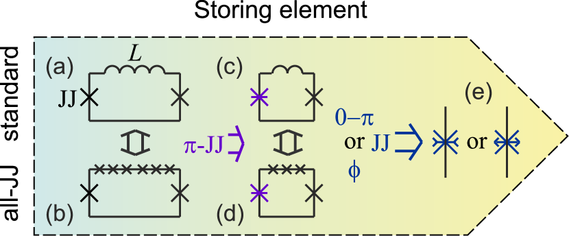
The functioning of superconducting logic circuits is based on the effect of magnetic flux quantization, instead of the modulation of conductance [6, 7]. This allows a discrete representation of information in the form of a Single Flux Quantum (SFQ), (where is the Planck constant, is the electron charge). The basic element of the broadly used Rapid Single Flux Quantum (RSFQ) [12] logic is a superconducting loop interrupted by Josephson junctions, see Fig. 1(a). If the loop inductance, , is high enough such that (where is the JJ critical current) then an SFQ can be hold in the loop representing logical unity, while an absence of an SFQ means logical zero.
In this paper, we consider different approaches for miniaturization of RSFQ basic cell. This includes the analysis of the scalability of the inductor, the substitution of the inductor by Josephson junctions, and the utilization of magnetic JJs of various kinds. The latter ends with the possibility of replacing the basic cell with a single bistable Josephson junction (see Fig. 1). We complement this with a proposition of a design methodology for superconducting circuits without inductors based on bistable JJs. Our design is based on a basic block. Modification and complication of its schematic allow obtaining various logic cells. We demonstrate the validity of the proposed methodology using the design of an 8-bit parallel adder as an example. We conclude the article with a brief discussion of the obtained results and outlining further research directions.
II Miniaturization of basic cell
II.1 Scaling of inductor
Theoretical estimation [13] of the maximum density of SFQ-based circuits utilizing geometrical inductance of wires gives already achieved JJ/cm2. The further decrease of the linewidth and spacing is problematic because of a nearly exponential growth in the mutual inductance and cross-talk between the inductors [14]. The main approach to shrink the inductor is related to the utilization of kinetic inductance. Here the energy stored in the inductor corresponds to the kinetic energy of the superconducting current, not to the magnetic field around a wire. The critical current of the inductor, , must be greater than that of a Josephson junction, which in turn should be much greater than the noise current, (where is the Boltzmann constant), to provide low bit error rate. The noise current at the operation temperature K is A. The typical value of the Josephson junction critical current is mA so that the inductance of a storing cell is pH.
For a real type-II superconductor film with the width, , being much larger than the coherence length, , the wire critical current, , is a fraction of Ginzburg-Landau (GL) depairing critical current, [15, 16]. Here, is the thickness of the wire, is the London magnetic penetration depth, and is the vacuum permeability. The critical current reduction [14], , is caused by the entry and motion of Abrikosov vortices from the film edges.
The kinetic inductance of a thin wire is , where is the wire length, . The required cell inductance, . The critical current of the inductor must also be greater than the JJ, so . Therefore, the minimum wire length and its cross-section area are determined by the chosen material and the quality of the wire edges. For a reasonable ratio, , and some “dirty” superconductor like MoNx, NbTiN or NbN with high kinetic inductance (where nm, nm, nm [14]), the wire geometrical parameters are m and nm2.
If the wire width is equal to the minimum feature size of a standard SFQ5ee MIT LL process technology, nm, the wire thickness is nm so that the wire cross-section aspect ratio is . The area of the kinetic inductor is m2, which is close to the typical area of a Josephson junction, m2. The inductor implementation requires about 2.5 squares with the inductance per square, pH. The obtained numbers show that the utilization of the kinetic inductance is a good solution for the current technological processes.
However, the convenience of utilization of the kinetic inductance at smaller scales is questionable. For example, the reduction of the inductor width down to nm requires the increase in its thickness up to nm (if the length is m) to preserve its critical current. Here the wire cross-section aspect ratio is that presents a difficulty for fabrication. At the same time, the inductance per square becomes four times smaller so that the implementation of the inductor is much less effective in the new scale. A safe threshold for the kinetic inductor scaling is about nm, which provides a square cross-section of the wire. Based on the presented estimations, we conclude that the basic cell scaling requires further research of alternative methods.
II.2 Superconducting loop without inductor
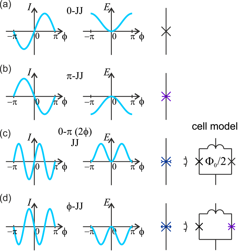
If an SFQ is inside the standard cell shown in Fig. 1(a), the Josephson phase of one of the junctions is close to (where is an integer) while the phase of another one is about , so that the total phase increment in the circuit is . These Josephson phase values correspond to minima of conventional superconductor - insulator - superconductor JJ (0-JJ hereinafter) Energy-Phase Relation (EPR), , where is the Josephson phase, and is the Josephson energy, see Fig. 2(a). This EPR corresponds to a sinusoidal Current-Phase Relation (CPR), , where is the current flowing through the junction.
Josephson junctions in the storing cell can be connected by a stack of JJs instead of an inductor [17, 18], see Fig. 1(b). Such cell can be called all Josephson junction (all-JJ) circuit. If the critical currents of the JJs in a stack are identical, the phase drop on each of them is , where is the number of the JJs in the stack. To prevent the JJs from switching, this phase drop should be less than (in accordance with 0-JJ CPR). Reliable operation of circuits is supposed to be provided with the phase drop about [17]. This gives 6 JJs in a stack that can be implemented, e.g., using two 3-JJ stacks [18].
II.3 Josephson junction
The issue of a rather large number of JJs in a stack can be mitigated by the introduction of the JJ having ferromagnetic interlayer in its weak-link region providing phase shift of its CPR, (-JJ hereinafter) [19, 20]. -JJ CPR and EPR are presented in Fig. 2(b). The -JJ symbol is a cross with a dash in the middle. With a -JJ in a loop, the phase increment corresponding to magnetic half flux quantum already exists in the cell. The cell inductance can be reduced correspondingly, and the number of JJs in the substituting stack can be decreased down to 3, see Fig. 1(c),(d) [21, 22, 23, 24, 25, 26, 27, 28, 29]. In RSFQ Toggle (T) flip-flop, it is possible even to completely substitute the inductor by a -JJ [21, 22, 23]. Unfortunately, this can’t be a general solution for all circuits. The constraints of this method come from the persistent current arising due to the -JJ inherent phase shift. This current outflows into the neighboring cells and may alter their power supply and break their operation. The direction of this current is determined by the circuit state and thus can’t be compensated with constant bias current adjustment.
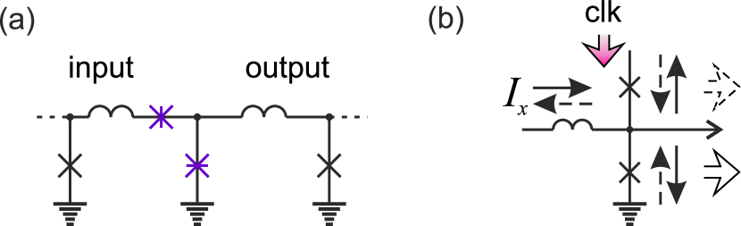
A design methodology utilizing two -JJs connected in series was proposed to circumvent this issue [25]. Fig. 3(a) illustrates the idea. Here the Josephson phase of each of the -JJs is about while the one on the 0-JJ in the input circuit is about ; combined, the phase shift is , allowing a state with and thus zero phase shift and zero current (see also Fig. 2(a),(b)). This allows the safe connection of the circuit input to conventional RSFQ cells. At the same time, phase drop on the central -JJ makes 0-JJ of the output loop being outside the minimum of its potential energy. Minimization of the total energy of the - and 0-JJ leads to the states with a noticeable current in the output loop, which can have opposite directions. This provides the opportunity to read out the circuit state by using conventinal balanced comparator shown in Fig. 3(b) [12]. The latter is two JJs connected in series, one of which is switched by the clock (clk) pulse depending on the direction of the measured current, . Many broadly used cells like a Delay (D) flip-flop and Non-Destructive Read-Out (NDRO) [25], logical AND, and OR cells [26] are designed in the frame of this approach.
II.4 Bistable Josephson junctions
The main requirement for a storing cell is the existence of two stable states: with and without an SFQ inside. However, the desired bistability can be obtained even with a single bistable Josephson junction. In this case, the storing element of the circuits reduces to this single JJ, and its state doesn’t relate to an SFQ.
The bistability corresponds to the existence of the second harmonic in the JJ CPR, . If , the EPR has a double-well shape [30]. In the case of the positive second harmonic amplitude, , the JJ energy minima are located at 0 and phase values [30]. This junction is called JJ, correspondingly [31, 32, 33]. Note that the vanishing of the first harmonic here leads to the doubling of the CPR. In this case, the JJ is called -JJ [34, 35, 36, 37, 38]. If the second harmonic amplitude is negative, , the JJ energy minima is symmetrically located around zero at phases, where [30]. This JJ is called -JJ [39, 40, 41, 42, 43, 33]. CPR and EPR of and -JJ for the case of suppressed first harmonic in their CPR are presented in Fig. 2(c),(d). The symbols of the JJs are similar to the one of the -JJ but with arrows added in the ends of the central dash directed inside or outside for and -JJ, correspondingly.
The considered bistable junctions are relatively new types of JJs. They are not introduced in digital superconducting technology yet. While the optimal method for their fabrication is a technological challenge, they can be already modeled using cells composed of standard junctions [44]. The model of -JJ is a superconducting loop with two 0-JJs and a Half Flux Quantum (HFQ) applied to the cell, see Fig. 2(c) [30]. The cell has a small but finite inductance. The smaller the inductance, the smaller is the cell critical current and the closer is the cell CPR to the doubled sine. Here the decrease of the first harmonic amplitude is caused by the circulating current induced by HFQ, while the second harmonic amplitude, and hence the effective critical current of the junction, is determined by the inductance.
In a very similar way, a -JJ can be modeled by a cell with 0- and -JJ, see Fig. 2(d) [30]. It was shown that Josephson Transmission Line (JTL) composed of such cells (modeling -JJs) is capable to transmit HFQ [27, 28, 29]. The transfer to manipulation with HFQ instead of SFQ makes the HFQ circuits to be more power-efficient than all other superconducting logic circuits [29]. Note that the small inductance in the cell model can be substituted by 0-JJs to obtain all-JJ circuit [30].
The utilization of bistable JJs seems promising in the aspects of power and space efficiency. Below we propose a design methodology for the circuits without inductors based on bistable -JJs. The latter are chosen because their cell model contains only conventional 0-JJs, see Fig. 2(c). Since the proposed design requires only two types of JJs, the conventional 0-JJs and bistable -JJs, this simplifies the experimental verification of prototype circuits. The information bit in the circuits is represented as a presence or absence of a superconducting phase change. This phase change can be transferred along the circuit by the application of the bias current.
III Design methodology
III.1 Basic block
The dynamics of the -JJ, as well as 0-JJ, is described by the well-known Resistive Shunted Junction model with Capacitance (RSJC) [45] (see also [30] for details):
| (1) |
where current flowing through the junction, , and the amplitudes of CPR harmonics, , are normalized to the critical current of a reference junction, , dots mean derivatives with respect to the time, , normalized to the inverse plasma frequency, , which is determined by the constants of a certain fabrication process, , where is the critical current density of Josephson junctions and is their specific capacitance, is the Josephson junction damping coefficient, and is the junction characteristic frequency, is the junction resistance in the normal state.
Each type of the considered junctions has only one harmonic dominating in the CPR. Therefore, the dominating harmonic determines the critical current of the junction. Since the circuits consist of the JJs only and each JJ has only two parameters, the critical current and the damping coefficient [30], these parameters determine the circuit dynamics. The former reflects the strength of superconducting coupling determining the potential barrier for the JJ switching, while the latter reflects the duration of the switching.

The proposed circuits are based on the basic block designed in accordance with the methodology presented in [25]: the input loop is in a current-less state, while the different phases of the -JJ correspond to the different currents circulating in the output loop.
The input loop is composed from one 0- and two -JJs, see Fig. 4(a). The phase drop on the 0-JJ is distributed among -JJs meaning the phase drop multiple of on each of them. This corresponds to the current-less state of the loop due to CPRs of the used JJs, see Fig. 2. Therefore the loop can be connected to other circuits from the side of 0-JJ.
A circulating current in the circuit with two 0-JJs and one -JJ, see Fig. 4(b), corresponds to phase drop on the latter one. At the same time, phase drop on -JJ provides the current-less state. Combination of the two considered loops (Fig. 4(a),(b)) forms our basic block, see Fig. 4(d).
In our simulations, we utilize all-JJTLs to apply and read out superconducting phase changes to/from the circuits. These are the JTLs in which each inductor is substituted for a single Josephson junction, see all-JJTL cell in Fig. 4(c). Parameters of the circuits, as well as a detailed description of their dynamics, are presented in supplemental materials [30].
The logical state of the basic block corresponds to the Josephson phase of the main -JJ, , located in the center of the circuit (Fig. 4(d)). parameters are depicted on () plane in Fig. 5(a) by a star as a reference point. The superconducting phase change wave enters the basic block through the junction and can exit through . The interconnecting junctions, and , serve as the input and output valves in the wave transfer process.
The block possesses four modes of operation in dependence of the input valve junction, , parameters () as it is presented in Fig. 5(a): (1) - terminator, (2) transmission line, (3) digital frequency divider, and (4) oscillator. In a trivial case where the junction is sufficiently “weaker” and “faster” than the main junction , the input phase change switches and exits through (mode 1). In the opposite case, the input wave passes through switching it twice and exits through (mode 2).
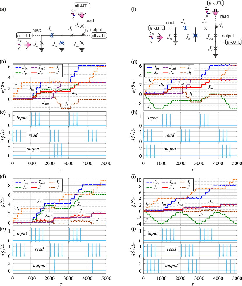
More interesting modes of operation are obtained at the mixed ratio of parameters of the -JJs. If the input valve junction is “weaker” than the main junction it starts to switch first. But if its switching takes a relatively long time, the main junction also has time to switch (see Fig. 5(b)). In this way, the incoming phase change is transformed into phase increase on each of the -JJs. Since the output junction has a periodic CPR, every second phase change wave passes through the basic block. Here the block operates as a digital frequency divider like a T flip-flop (mode 3), see Fig. 5(b),(c).
Simultaneous switching of the -JJs occurs in a relatively wide range of ratios of their parameters (including the inverse ratio with the corresponding swap in the sequence of their switchings). Interestingly, increase of the input valve junction critical current results in another operation regime. Here leakage of the interface all-JJTL bias current into provides its periodic switching if phase is about . These switchings of can be turned on and off by the switching of the logic state of the basic block. In this mode 4, the block operates as a conventional SFQ-to-DC converter [12]., see Fig. 5(d),(e).
III.2 Controlled readout of -JJ states
Controlled readout of the circuit logical state can be performed if the output of the basic block is designed as a balanced comparator (see Fig. 3(b) [12]). In this case, another 0-JJ, , is connected to the output loop, accordingly, see Fig. 6(a). Read phase change wave is applied to the pair of junctions, , .
The Non-Destructive Read-Out (NDRO) is realized when the processes in the output loop do not significantly affect . At the same time, the phase is increased by about with every phase change wave coming from the input loop. The circuit operation is close to the modes 3, 4 considered above but here the input wave never passes to the output. The direct passages of the waves from the input to the output and backward are blocked by making the output valve junction, , “weak” and “fast” compared to the neighboring junctions, , . Dynamics of Josephson junctions and voltage pulses corresponding to the propagation of the phase change waves in the input, read and output all-JJTLs are presented in Fig. 6(b),(c).
One can switches from NDRO operation to the Destructive Read-Out (DRO) by changing the output valve junction, , parameters; namely, making it slower. The DRO is implemented when the only first input phase change wave increases phase by about . Another increase is available only with the read wave. Since is connected to , the slower phase increase in the point of their connection allows to switch twice with every input phase change wave if phase is about , see [30]. At the same time, with a slowdown of , has time to switch from the state while phase increases by . The DRO cell operates as a D flip-flop, see Fig. 6(d),(e).
Note that the read data can be easily inverted. This is achieved by a simple swap of , connection order, see Fig. 6(f). In this case, and are connected to the ground through . Thus, the stationary distribution of the currents and dynamics of the junctions become changed so that the circuit parameters require an additional adjustment, see [30]. Simulation of dynamics of NDRO and DRO cells with output inversion is presented in Fig. 6(g),(h) and Fig. 6(i),(j), correspondingly. The DRO cell here performs synchronous data inversion that is the logical NOT operation.
III.3 Example of a cell design
We presented only a simple combination of the input and output circuits to write/read the logical state encoded in a -JJ phase so far. Functionality of a cell can be increased by connection of additional branches. For example, NDRO output jointed with DRO cell forms NDRO cell with separate inputs to set/reset the latch, see Fig. 7(a). Additional output interface circuit providing NDRO is circled by a dotted line. Josephson junctions of this circuit are marked by capital “R” in their subscripts. Designation of the other Josephson junctions are inherited from Fig. 6(a). phase change wave entering the cell through switches the logical state by increasing the phase by , while the one entering the cell through resets the state back. The critical current of the Josephson junction connecting NDRO branch to DRO cell is made small to make these parts decoupled.
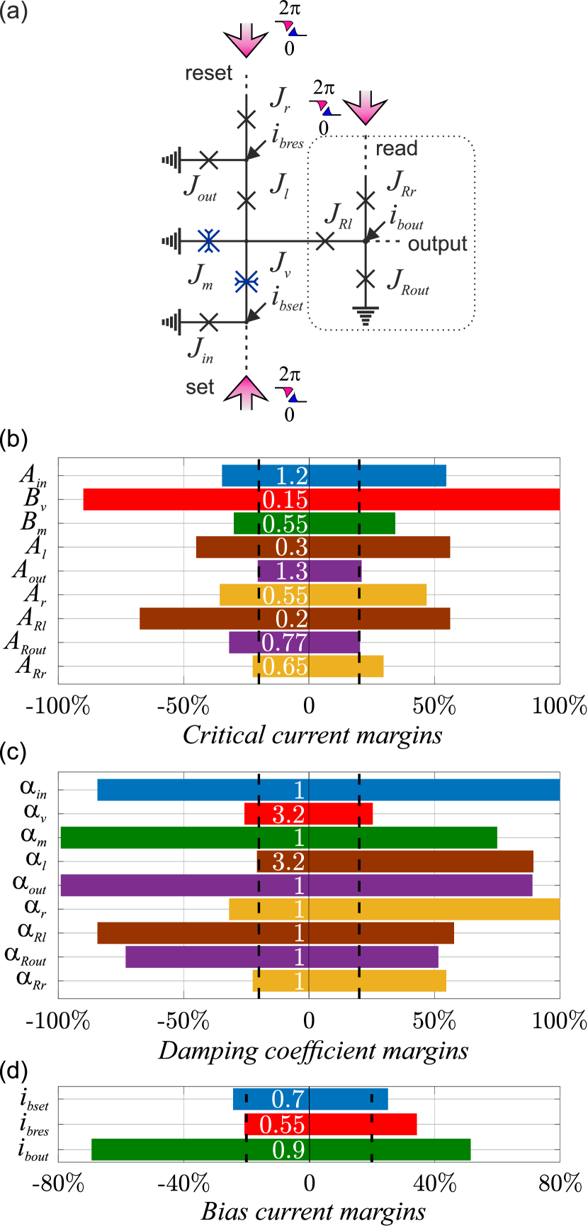
In the design of this cell, we divide all the JJs into “fast” and “slow” ones, having a correspondingly small or large value of the damping coefficient, see Fig. 7(c). After optimization procedure, we find that the working margins of the bias currents, as well as of parameters of the Josephson junctions, are greater than at low-speed test, see Fig. 7(b)-(d). The margins are expected to shrink with the operation frequency increase.
We add a small parasitic inductance in series to every Josephson junction of the considered circuit to examine its effect. The normalized inductance value is (1.65 pH for mA). While the values of parameters become clearly shifted, after additional optimization procedure the working margins are restored to upper than . This illustrates the importance of careful extraction of parameters of the circuits from layout as well as overall robustness of the proposed design approach to existence of the parasitic inductors.
III.4 Benchmark logic circuit design
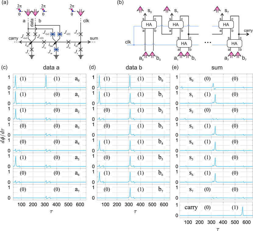
We verify the validity of the proposed design methodology on the example of the design of an 8-bit parallel adder. The basic element of this adder is a half-adder (HA) presented in Fig. 8(a). Here the phase of the main -JJ, , is changed by every phase change wave coming from the data lines or through junctions. The interface circuit of the output sum () provides destructive readout of the state. The interface circuit of the output carry () provides a non-destructive readout of the state before it is changed by the data phase change waves. Therefore, the carry readout is asynchronous with respect to clock. Note that data can flow sequentially or simultaneously to the HA cell. In the last case the output junction of the carry branch, , is switched due to the total effect of the two phase change waves. This is similar to the operation of RSFQ AND cell [12]. Parameters of the half-adder JJs are presented in Table II in [30].
Note that just a single -JJ is sufficient here to provide the data storage. This is in contrast to RSFQ HA where insensitivity to the data delay comes at the cost of doubling the SFQ storage circuit [46]. Thus, the number of JJs in the presented schematic is even smaller than in the RSFQ counterpart despite the substitution of inductors for JJs.
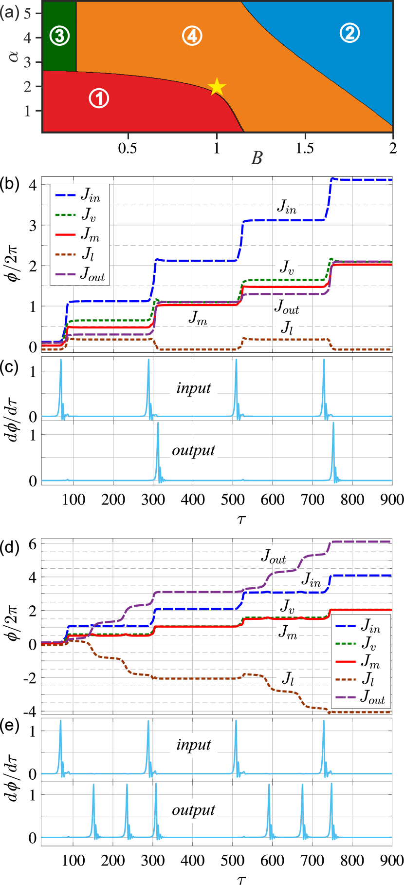
An 8-bit ripple-carry wave pipeline adder schematic is presented in Fig. 8(b). Its energy-efficient RSFQ (ERSFQ [47]) counterpart was proposed earlier as a process benchmark [48]. For -bit circuit one needs HA cells connected in our case by all-JJTLs and all-JJ confluence buffers (CBs). The total number of JJs in the adder is 362 with 150 JJs in HAs (10 JJs per HA), and 212 JJs in all-JJTLs and CBs. An additional 150 JJs are in the clock distribution network. The summation operation is performed in a single clock cycle [48] with the total time delay (normalized to the inverse plasma frequency), . The output data front is aligned, meaning that the less significant and the most significant bits are produced simultaneously.
Circuit operation was simulated with various inputs. Voltage pulses corresponding to the phase change waves in and data branches as well as in the sum branches are shown in Fig. 8(c),(d),(e), correspondingly. The last bottom panel in Fig. 8(e) shows the output carry. The first example presents the summation of two randomly chosen numbers: (39) and (83) that results in the sum (122). The second example corresponds to the longest propagation of carry: (1) and (255) that results in the sum and generation of the output carry (256).
IV Discussion
With the presented utilization of -JJs one can easily mimic the behaviour of RSFQ circuits due to a certain -JJ CPR. However, other types of bistable junctions are also suitable. Using 0- JJs instead of -JJs in the basic block would result in some shrinking of operation margins caused by lesser depth of the potential well at . Using -JJs with potential energy minima at would additionally lead to some finite current in the output interface circuit in both states of the -JJ. Still, correct circuit operation is possible using these alternative implementations [25].
A nonzero first harmonic in the CPR provides two critical currents of the bistable JJ. This is due to the different heights of potential barriers between the EPR minima. The difference in the critical currents gives an opportunity to read out the state directly from the junction [42]. This could serve for further simplification of the schematics.
Logical zero and unity correspond to zero and phase changes in the presented circuits. At the same time, the operation of the cells is based on the transformation of the phase change into phase drops on the bistable JJs. One can consider an option for a more complex information processing with propagation of phase change waves. This includes a possibility of ternary logic circuit design. Three options of the logical states can be associated with zero, , and phase changes. Manipulation with phase change waves instead of ones can additionally increase the power-efficiency [29].
The utilization of bistable JJs eliminates the need for SFQ storage and hence the necessity for technological implementation of the quantizing inductance. The inductor can be used as an interconnecting element or not used at all. The latter leads to the fact that the circuit characteristics are determined only by the parameters of the Josephson junctions. Our results show that the all-JJ circuits can be designed using just a few values of JJ damping, which is promising for their implementation. While circuits without inductors can be implemented with more conventional 0- and -JJs, utilization of bistable Josephson junctions significantly decreases the total JJ count.
We have shown that the all-JJ cells can be connected by all-JJTLs. However, the utilization of passive transmission lines (PTLs) looks more promising for long-range connections. It was shown that PTLs are suitable for high-density routing with low cross-talk allowing fast data transfer and precision timing design of the circuits [49, 50]. The cells can be even connected by PTLs only [51], though with a relatively large width of PTLs this option poses certain limits on the integration density.
While the considered bistable JJs can be readily modeled with simple two-JJ cells [30], the full advantage from their utilization can be gathered with their fabrication as a solid heterostructure. Therefore, the development of corresponding fabrication methods suitable for large scale integrated circuits would be of significant benefit.
V Conclusion
In summary, we considered different options for the implementation of the basic storing element of superconducting circuits. We argued that the use of inductors in conventional designs presents technological problems for circuit deep scaling. The utilization of bistable Josephson junction as a storing element looks promising in this context. In this case, magnetic flux is not used as the physical representation of information. This eliminates the requirements posed on inductors including the possibility to completely get rid of them. We presented the design methodology of the circuits without inductors based on bistable Josephson junctions. The methodology was used in the design of various basic cells like controlled oscillator analogous to conventional SFQ-to-DC converter, T flip-flop, D flip-flop, NDRO, logical NOT, and half adder. A more complex benchmark logic circuit of an 8-bit parallel adder was designed as well. Working margins of the all-JJ NDRO cell with small parasitic inductances at low-speed test exceed in simulations. The cell was designed using just a couple of values of the JJ damping coefficient, which is favorable for its implementation. The design of the half adder cell has shown that the total number of JJs in the all-JJ circuits can be less than in the standard design. We concluded that the proposed utilization of bistable Josephson junctions is promising in the aspects of the elimination of the need for quantizaing inductance, possible simplification of the all-JJ circuit schematics, and the reduction of total JJ count leading to space-efficiency. The search for technological routes for the bistable JJ fabrication and the development of information processing methods using circuits based on such junctions are urgent tasks in this area of research.
Acknowledgements.
The authors are grateful to D. S. Holmes for fruitful discussions. The development of the all-JJ circuit design methodology was performed under the support of grant No. 20-12-00130 of the Russian Science Foundation. The review of the scalability of superconducting inductor was supported by the grant of the President of the Russian Federation MD-186.2020.8. Design of an 8-bit parallel adder was supported by RFBR grant No. 19-32-90208. V.I.R. acknowledges the Basis Foundation scholarship. N.V.K. and M.Yu.K. are grateful to the Interdisciplinary Scientific and Educational School of Moscow University “Photonic and Quantum Technologies. Digital Medicine”.References
- Moore [2003] G. E. Moore, No exponential is forever: but ”Forever” can be delayed!, in IEEE International Solid-State Circuits Conference, 2003. Digest of Technical Papers. ISSCC (2003).
- Takeuchi et al. [2015a] N. Takeuchi, Y. Yamanashi, and N. Yoshikawa, Energy efficiency of adiabatic superconductor logic, Supercond. Sci. Technol. 28, 015003 (2015a).
- Takeuchi et al. [2013] N. Takeuchi, Y. Yamanashi, and N. Yoshikawa, Measurement of 10 zJ energy dissipation of adiabatic quantum-flux-parametron logic using a superconducting resonator, Appl. Phys. Lett. 102, 052602 (2013).
- Holmes et al. [2013] D. S. Holmes, A. L. Ripple, and M. A. Manheimer, Energy-efficient superconducting computing - power budgets and requirements, IEEE Trans. Appl. Supercond. 23, 1701610 (2013).
- Soloviev et al. [2017] I. I. Soloviev, N. V. Klenov, S. V. Bakurskiy, M. Y. Kupriyanov, A. L. Gudkov, and A. S. Sidorenko, Beyond Moore’s technologies: operation principles of a superconductor alternative, Beilstein J. Nanotechnol 8, 2689 (2017).
- Mukhanov [2011] O. A. Mukhanov, Energy-efficient single flux quantum technology, IEEE Trans. Appl. Supercond. 21, 760 (2011).
- Herr et al. [2011] Q. P. Herr, A. Y. Herr, O. T. Oberg, and A. G. Ioannidis, Ultra-low-power superconductor logic, J. Appl. Phys. 109, 103903 (2011).
- Takeuchi et al. [2015b] N. Takeuchi, Y. Yamanashi, and N. Yoshikawa, Energy efficiency of adiabatic superconductor logic, Supercond. Sci. Technol. 28, 015003 (2015b).
- [9] E. P. DeBenedictis, New design principles for cold, scalable electronics, http://www.debenedictis.org/erik/Cryo_FPGA_2LAL/DPfC_51.pdf.
- Bhushan et al. [2020] M. Bhushan, P. Bunyk, M. Cuthbert, E. DeBenedictis, R. L. Fagaly, P. Febvre, C. Fourie, M. Frank, D. Gupta, A. Herr, D. S. Holmes, T. Humble, A. L. de Escobar, C. McGeoch, N. Missert, P. Mueller, O. Mukhanov, K. Nemoto, S. P. Rao, B. Patra, B. Plourde, N. Pugach, B. Tyrrell, T. Vogelsang, F. Wilhelm-Mauch, and N. Yoshikawa, IRDS 2020: Cryogenic Electronics and Quantum Information Processing, https://irds.ieee.org/editions/2020 (2020), part of IEEE International Roadmap for Devices and Systems.
- Tolpygo et al. [2020] S. K. Tolpygo, V. Bolkhovsky, R. Rastogi, S. Zarr, E. Golden, T. J. Weir, L. M. Johnson, V. K. Semenov, and M. A. Gouker, A 150-nm node of an eight-Nb-layer fully planarized process for superconductor electronics, in Applied Superconductivity Conference 2020 (2020).
- Likharev and Semenov [1991] K. K. Likharev and V. K. Semenov, RSFQ logic/memory family: A new Josephson-junction technology for sub-terahertz-clock-frequency digital systems, IEEE Trans. Appl. Supercond. 1, 3 (1991).
- Tolpygo et al. [2018a] S. K. Tolpygo, V. Bolkhovsky, R. Rastogi, S. Zarr, A. L. Day, T. J. Weir, A. Wynn, and L. M. Johnson, Developments toward a 250-nm, fully planarized fabrication process with ten superconducting layers and self-shunted Josephson junctions, in 2017 16th International Superconductive Electronics Conference (ISEC) (2018).
- Tolpygo et al. [2018b] S. K. Tolpygo, V. Bolkhovsky, D. E. Oates, R. Rastogi, S. Zarr, A. L. Day, T. J. Weir, A. Wynn, and L. M. Johnson, Superconductor electronics fabrication process with MoNx kinetic inductors and self-shunted Josephson junctions, IEEE Trans. Appl. Supercond. 28, 1100212 (2018b).
- Ginzburg and Landau [1950] V. L. Ginzburg and L. D. Landau, On the theory of superconductivity, Zh. Experim. i Teor. Fiz. 20, 1064 (1950), (Transl.: in V. L. Ginzburg, On Superconductivity and Superfluidity. A Scientific Autobiography, Berlin, Germany: Springer, 2009, pp. 113-137).
- Kupriyanov and Lukichev [1980] M. Y. Kupriyanov and V. F. Lukichev, Temperature dependence of pair-breaking current in superconductors, Fizika Nizkikh Temperatur 6, 445 (1980).
- Tolpygo [2016] S. K. Tolpygo, Superconductor digital electronics: Scalability and energy efficiency issues, Low Temp. Phys. 42, 361 (2016).
- Castellanos-Beltran et al. [2019] M. A. Castellanos-Beltran, D. I. Olaya, A. J. Sirois, P. D. Dresselhaus, S. P. Benz, and P. F. Hopkins, Stacked Josephson junctions as inductors for single flux quantum circuits, IEEE Trans. Appl. Supercond. 29, 1300705 (2019).
- Ryazanov et al. [2001] V. V. Ryazanov, V. A. Oboznov, A. Y. Rusanov, A. V. Veretennikov, A. A. Golubov, and J. Aarts, Coupling of two superconductors through a ferromagnet: Evidence for a junction, Phys. Rev. Lett. 86, 2427 (2001).
- Golubov et al. [2004] A. A. Golubov, M. Y. Kupriyanov, and E. Il’ichev, The current-phase relation in Josephson junctions, Rev. Mod. Phys. 76, 411 (2004).
- Ustinov and Kaplunenko [2003] A. V. Ustinov and V. K. Kaplunenko, Rapid single-flux quantum logic using -shifters, J. Appl. Phys. 94, 5405–7 (2003).
- Ortlepp et al. [2006] T. Ortlepp, A. Ariando, O. Mielke, C. J. M. Verwijs, K. F. K. Foo, H. Rogalla, F. H. Uhlmann, and H. Hilgenkamp, Flip-flopping fractional flux quanta, Science 312, 1495–7 (2006).
- Khabipov et al. [2010] M. I. Khabipov, D. V. Balashov, F. Maibaum, A. B. Zorin, V. A. Oboznov, V. V. Bolginov, A. N. Rossolenko, and V. V. Ryazanov, A single flux quantum circuit with a ferromagnet-based Josephson -junction, Supercond. Sci. Technol. 23, 045032 (2010).
- Ortlepp et al. [2007] T. Ortlepp, A. Ariando, O. Mielke, C. J. M. Verwijs, K. F. K. Foo, A. Andreski, H. Rogalla, F. H. Uhlmann, and H. Hilgenkamp, RSFQ circuitry using intrinsic -phase shifts, IEEE Trans. Appl. Supercond. 17, 659–64 (2007).
- Yamanashi et al. [2018] Y. Yamanashi, S. Nakaishi, A. Sugiyama, N. Takeuchi, and N. Yoshikawa, Design methodology of single-flux-quantum flip-flops composed of both 0- and -shifted Josephson junctions, Supercond. Sci. Technol. 31, 105003 (2018).
- Yamanashi et al. [2019] Y. Yamanashi, S. Nakaishi, and N. Yoshikawa, Simulation of the margins in single flux quantum circuits containing -shifted Josephson junctions, IEEE Trans. Appl. Supercond. 29, 1301805 (2019).
- Kamiya et al. [2018] T. Kamiya, M. Tanaka, K. Sano, and A. Fujimaki, Energy/space-efficient rapid single-flux-quantum circuits by using -shifted Josephson junctions, IEICE Trans. Electron. E101-C, 385 (2018).
- Hasegawa et al. [2019] D. Hasegawa, Y. Takeshita, K. Sano, M. Tanaka, A. Fujimaki, and T. Yamashita, Magnetic Josephson junctions on Nb four-layer structure for half flux quantum circuits, in 2019 IEEE International Superconductive Electronics Conference (ISEC) (2019).
- Li et al. [2021] F. Li, Y. Takeshita, D. Hasegawa, M. Tanaka, T. Yamashita, and A. Fujimaki, Low-power high-speed half-flux-quantum circuits driven by low bias voltages, Supercond. Sci. Technol. 34, 025013 (2021).
- [30] See supplementary material for details on CPRs of bistable Josephson junctions, their cell models, and our numerical calculation of circuits.
- Goldobin et al. [2003] E. Goldobin, D. Koelle, and R. Kleiner, Ground states and bias-current-induced rearrangement of semifluxons in 0- long Josephson junctions, Phys. Rev. B 67, 224515 (2003).
- Zenchuk and Goldobin [2004] A. Zenchuk and E. Goldobin, Analysis of ground states of 0- long Josephson junctions, Phys. Rev. B 69, 024515 (2004).
- Bakurskiy et al. [2017] S. V. Bakurskiy, V. I. Filippov, V. I. Ruzhickiy, N. V. Klenov, I. I. Soloviev, M. Y. Kupriyanov, and A. A. Golubov, Current-phase relations in SIsFS junctions in the vicinity of 0- transition, Phys. Rev. B 95, 094522 (2017).
- Trifunovic [2011] L. Trifunovic, Long-range superharmonic Josephson current, Phys. Rev. Lett. 107, 047001 (2011).
- Richard et al. [2013] C. Richard, M. Houzet, and J. S. Meyer, Superharmonic long-range triplet current in a diffusive Josephson junction, Phys. Rev. Lett. 110, 217004 (2013).
- Pal et al. [2014] A. Pal, Z. H. Barber, J. W. A. Robinson, and M. G. Blamire, Pure second harmonic current-phase relation in spin filter Josephson junctions, Nat. Commun. 5, 3340 (2014).
- Baek et al. [2018] B. Baek, M. L. Schneider, M. R. Pufall, and W. H. Rippard, Anomalous supercurrent modulation in Josephson junctions with Ni-based barriers, IEEE Trans. Appl. Supercond. 28, 1800705 (2018).
- Stoutimore et al. [2018] M. J. A. Stoutimore, A. N. Rossolenko, V. V. Bolginov, V. A. Oboznov, A. Y. Rusanov, N. Pugach, S. M. Frolov, V. V. Ryazanov, and D. J. V. Harlingen, Second-harmonic current-phase relation in Josephson junctions with ferromagnetic barriers, Phys. Rev. Lett. 121, 177702 (2018).
- Pugach et al. [2010] N. G. Pugach, E. Goldobin, R. Kleiner, and D. Koelle, Method for reliable realization of a Josephson junction, Phys. Rev. B 81, 104513 (2010).
- Klenov et al. [2010] N. V. Klenov, N. G. Pugach, A. V. Sharafiev, S. V. Bakurskiy, and V. K. Kornev, Josephson junctions with nonsinusoidal current-phase relations based on heterostructures with a ferromagnetic spacer and their applications, Phys. Solid State 52, 2246 (2010).
- Sickinger et al. [2012] H. Sickinger, A. Lipman, M. Weides, R. G. Mints, H. Kohlstedt, D. Koelle, R. Kleiner, and E. Goldobin, Experimental evidence of a Josephson junction, Phys. Rev. Lett. 109, 107002 (2012).
- Goldobin et al. [2013] E. Goldobin, H. Sickinger, M. Weides, N. Ruppelt, H. Kohlstedt, R. Kleiner, and D. Koelle, Memory cell based on a josephson junction, Appl. Phys. Lett. 102, 242602 (2013).
- Bakurskiy et al. [2013] S. V. Bakurskiy, N. V. Klenov, T. Y. Karminskaya, M. Y. Kupriyanov, and A. A. Golubov, Josephson -junctions based on structures with complex normal/ferromagnet bilayer, Supercond. Sci. Technol. 26, 015005 (2013).
- Goldobin et al. [2015] E. Goldobin, D. Koelle, and R. Kleiner, Tunable , , and Josephson junction, Phys. Rev. B 91, 214511 (2015).
- Stewart [1968] W. C. Stewart, Current‐voltage characteristics of Josephson junctions, Appl. Phys. Lett. 12, 277 (1968).
- Kirichenko [2002] A. F. Kirichenko, Universal delay-insensitive logic cell, US patent 6,486,694 B1 (2002).
- Kirichenko et al. [2011] D. E. Kirichenko, S. Sarwana, and A. F. Kirichenko, Zero static power dissipation biasing of RSFQ circuits, IEEE Trans. Appl. Supercond. 21, 776–779 (2011).
- Kirichenko et al. [2015] A. F. Kirichenko, I. V. Vernik, J. A. Vivalda, R. T. Hunt, and D. T. Yohannes, ERSFQ 8-bit parallel adders as a process benchmark, IEEE Trans. Appl. Supercond. 25, 1300505 (2015).
- Kitamura et al. [2020] K. Kitamura, M. Tanaka, T. Kawaguchi, I. Nagaoka, K. Takagi, A. Fujimaki, and N. Takagi, High-density routing with wire length matching for single-flux-quantum circuits using thin passive transmission lines, in Applied Superconductivity Conference 2020 (2020).
- Kashima et al. [2020] R. Kashima, I. Nagaoka, M. Tanaka, K. Sano, T. Yamashita, and A. Fujimaki, 50 GHz datapath for parallel SFQ microprocessors based on gate level pipeline architecture, in Applied Superconductivity Conference 2020 (2020).
- Whiteley et al. [2020] S. Whiteley, E. Mlinar, G. Krylov, T. Jabbari, E. Friedman, and J. Kawa, An SFQ digital circuit technology with fully-passive transmission line interconnect, in Applied Superconductivity Conference 2020 (2020).