Supplementary Information - Efficient and Continuous Microwave Photoconversion in Hybrid Cavity-Semiconductor Nanowire Double Quantum Dot Diodes
Supplementary Methods
Determination of the directivity term and DQD energies
The directivity of the DQD photodetector is given by the term , where is the so-called mixing angle, the detuning at resonance, the interdot tunnel coupling and the resonance frequency of the resonator Wong and Vavilov (2017); Childress, Sørensen, and Lukin (2004). To determine the directivity, we use the value obtained from the resonator response. To obtain the other parameter value, the detuning in resonance, we first determine how the left gate electrode changes the detuning based on finite bias transport measurements. Then based on identifying the detuning when the DQD is in resonance with resonator yields us both the detuning and the interdot coupling in the photodetector operation point. We present below the measurements and the procedure of these experiments in detail.
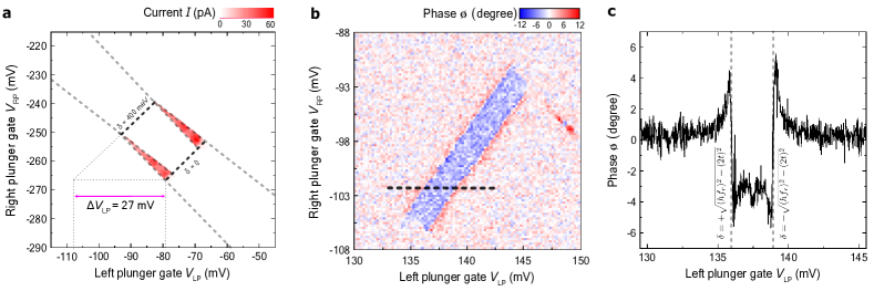
In Supplementary Fig. 1a, we present a finite bias measurement of the DQD. The bias voltage is set to via the resonator middle contact. From the finite bias triangles, we identify two detuning conditions Van der Wiel et al. (2002): at the base of the triangles the detuning vanishes, that is and the peaks of the two neighboring triangles define a detuning line corresponding to bias voltage, i.e. . These values are the minimum and maximum detuning values such that the energy levels are within the transport window and dc current flows. Since the gate voltages move the energy levels of the quantum dots up and down with a linear relation, measuring the distance in the left gate voltage direction denoted as in the figure, yields us the lever arm . This lever arm characterizes how much the left gate voltage shifts the detuning of the DQD. Here we have neglected the interdot tunnel coupling contribution to the total energy . This approximation is well justified since as we will see next.
Now we determine the and the interdot tunnel coupling based on the resonance condition . Here we use the full expression without the above approximation since with the resonator phase response to the DQD we are able to measure the small deviance that causes to the approximate relation used elsewhere in our data analysis. Supplementary Figures 1b and c, present the phase response of the resonator as a function of the DQD gates. We observe a response along the direction where the detuning changes while the response stays constant along the perpendicular direction similarly as in previous experiments Frey et al. (2012); Toida, Nakajima, and Komiyama (2013); Mi et al. (2017). We observe the resonance of the DQD with the microwave resonator as a sharp transition in the phase response. We have one resonance for positive detuning and one for negative detuning. Panel c shows a cut of the response with the left gate voltage . With that, we measure the distance of the positive and negative resonance condition . The resonance conditions result in a sharp transitions from a positive phase to a negative in the phase response. With the above lever arm, we convert this to the detuning at the resonance yielding us the directivity . With the total energy difference of the DQD in the resonance, , we also obtain the tunnel coupling as .
In Supplementary Fig. 1a, we see the first excited state with pronounced current in the middle of the triangles. The bias voltage opens up an energy window of . As the excited state is in the middle of it, we estimate the higher excited states of the quantum dots to be approximately above the states considered for the photodetector. Since this energy is an order of magnitude larger than the photon energy, and other energies in the system such as the thermal energy , the excited states of the quantum dots do not influence the photodetector operation.
Similar to the above determination of the detuning energies, we also determine the energy shifts along the detuning axis. This direction is identified by the base of the finite bias triangle where the energy difference of the ground and excited state is constant and the states are move up or down in energy in concert. The length of the triangle base in Supplementary Fig. 1a at corresponds to an energy shift of of the DQD energy levels. This allows us to determine the source-drain energy window of presented in Fig. 3a of the main manuscript.
Dark current
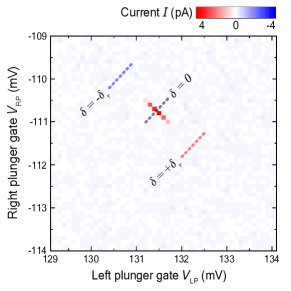
Supplementary Figure 2 presents the photodetector response with no applied microwave signal. We observe a miniscule signal at the charge triple point at . At the photodetector points , we see no measurable current. Thus, the dark current of the photodetector is below the 0.2 pA noise level of the measurement.
Charge configuration
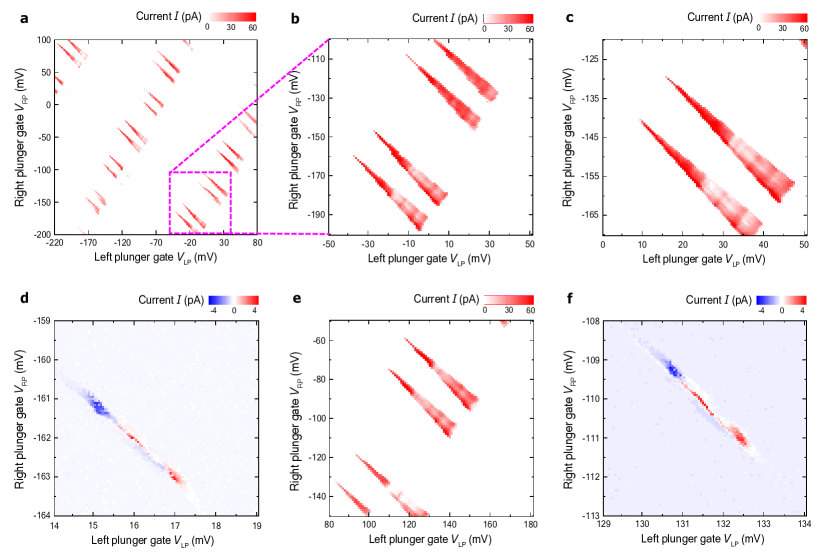
All the measurements presented in the article and in the Supplemental Material have been performed at the same charge configuration of the DQD. The plunger gate voltages vary from measurement to measurement due to slow drift of the offset charges (in a timescale of a week) that we followed during the course of the measurement. Supplementary Figure 3 summarises the measurements that we used for assuring to stay at the same operation point.
Supplementary Figure 3a presents an overview of the different charge numbers. Around each of the configurations, we observe a finite bias triangle pair with unique fingerprint. The magnitude of electrical current varies between each triangle with some having higher current at the base and other at the tip and some on the adjacent sides. Also, each one of them has a characteristic excited state spectrum forming lines along the triangles. The zoom-in of panel b presents the structure of the charge configuration we used throughout the manuscript at around and . Over the course of the measurements, we followed this charge transition point and made control measurement to check that we have the same charge transition whenever the configuration changed considerably. Supplementary Figures 3c and 3e show examples of these together with the repetition of the photodetection measurement of Fig. 3a of the main article in panels d and f correspondingly. We see the same features in the finite bias triangles as well as the same photoresponse at . Panels d and f have a stronger response to the positive current polarity only around as compared to the data in Fig. 3a of the main article. This arises as in these measurements the offset voltage of the current pre-amplifier was not tuned as well as for the data in the main article. It’s worth to note that the magnitude of the photoresponse at is unaltered as it is not sensitive to small bias voltages, i.e. if the chemical potential of either source or drain shift a little in the schematic diagram of Fig. 1a in the main article. We cannot for sure identify the origin of the current reversing response at of Fig. 3a in the main article. However, we speculate that it arises from a similar effect as reported in Ref. Cornia et al., 2019.
Determination of the microwave powers at the detector
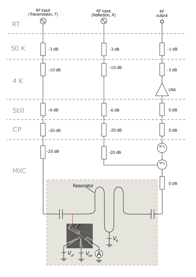
The microwave signals were sent in and the outcoming signals measured with a standard heterodyne detection scheme Lang (2014). The cabling in the cryostat is outlined in Supplementary Fig 4. Outside of the cryostat, the input signal from a RF generator was splitted into two parts. One of the signals was used as a phase reference mixed directly with a local oscillator (LO) and the second one was sent into the device via the cryostat and then mixed with the LO, digitized and then the amplitude and phase response was determined with digital signal processing by determining the amplitudes and phases at the IF frequency.
To determine the in and out going microwave powers at the device, we need to know the microwave attenuation in the signal lines. Supplementary Figure 4 outlines the microwave lines, their attenuators, amplifiers and circulators at each temperature stage. The connecting lines between different temperature stages are nominally identical in all the three lines. In addition to the identical connecting lines, we have the components listed in Supplementary Table 1. The input lines contain an extra cable, power splitter and attenuators in the cryostat. The output line, on the other hand, has a dual-circulator, cryogenic amplifier, attenuators but with lower losses, two room temperature (RT) amplifiers, mixer, intermediate frequency (IF) attenuation, amplifier and a low pass filter. We list the attenuation/gain for the components in the supplementary table, based on calibration datasheet (cryogenic amplifier) and the datasheet specifications (rest of the components). This leaves the attenuation of the cryostat cables as the only unknown that is out of construction the same for all lines.
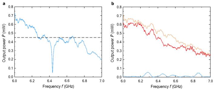
We determine close to the measurement frequency by measuring the reflection coefficient well off from the resonance frequency as presented in Supplementary Fig. 5a. The reflection coefficient off from the resonance is unity, i.e. all power is reflected back. By sending in a microwave signal and measuring a signal at the output yields us a total cable attenuation of when accounting for the components of the Supplementary Table 1. Since we have identical lines, half of these losses are at the input and half at the output and hence . The total attenuation from signal generator to the device is hence .
| Component | Attenuation/Gain at (dB) |
| Input lines: | |
| Output inter-connect cable, Minicircuits 086-36SM+ | |
| Power splitter, Minicircuits ZX10R-14-S+ | |
| Attenuators in the cryostat (Fig. 4) | |
| Cable losses | |
| Output line: | |
| Cryogenic circulator, LNF-CIISC4_8A, Insertion loss | |
| Cryogenic amplifier, LNF-LNC4_8C | |
| Cable losses | |
| Attenuators in the cryostat (Fig. 4) | |
| 2 x RT amplifier, Minicircuits ZX60-83LN12+ | |
| Attenuators at RT | |
| Mixer, Minicircuits ZMX-10G+, Conversion loss | |
| IF attenuator | |
| IF amplifier, Femto DLPVA | |
| LP filter attenuation |
In addition, to the components listed above, spurious losses could potentially alter the energy balance. The most relevant spurious losses are:
-
•
Extra connectors / interconnects in the output line for the circulator and amplifier: We use two Minicircuits 086-4SM+ cables for interconnects, one for the cryogenic amplifier and one for the circulator in the output port. These cables have an insertion loss of at GHz at room temperature. We anticipate that the losses at the operation temperature K is lower than this as the metals get more conducting towards lower temperatures. Hence these have in total less than dB (i.e. less than to the power balance) influence on the power balance calculation above. The extra SMA connectors are specified to have return loss that is better than dB. Hence the mismatch arising from the extra connectors is negligible (less than to the power balance).
-
•
Bonding wires: Bonding wires from the input and output ports to the printed circuit board connect the photodetector to the measurement setup. The bond wires can potentially cause attenuation and impedance mismatch to the circuit. To assess this, we measured a direct transmission line piece bonded instead of the photodetector to the measurement setup. The data is presented in Supplementary Fig. 5b. In this case we anticipate ideally full transmission and no reflected signal. We see that indeed, the transmitted signal in red follows the same background level as the fully reflected background signal in Supplementary Fig. 5a within or better. Also, the reflected signal is correspondingly suppressed to or below. Also the reflected signal without the probe (full reflection expected for disconnected probe) presents the same background level with slightly increased amplitude due to two 30 cm cables removed from the signal chain leading to lower overall losses. With these findings, we conclude that bonding wires influence the gain calculation by less than . It is also worth noting that the two ports are symmetric - also in terms of bonding - and hence the symmetric part of the possible attenuation from the bond wires is accounted for with the above attenuation determination.
-
•
Impedance mismatches: The input of the cryogenic amplifier has typically some amount of impedance mismatch that gives rise to part of the signal reflected back. Similarly, other components of the setup may cause reflections that give rise to standing waves. The setup is, however, build such that these standing waves are damped. For example for the input of the cryogenic amplifier, the reflected power goes to the circulators. They damp the reflected signal by 20 dB each making the reflected signals negligible. Similarly, the signal reflected from the input to the photodetector is damped by the attenuators of the input line. In the background signals presented in Supplementary Fig. 5 we observe that the oscillations arising from standing waves are below of the signal power. Similarly, the spuriously reflected signal of Supplementary Fig. 5b is below of the input signal. Note that here we have a frequency dependent attenuation that decreases the power towards higher frequencies, which is typical for microwave components. With these arguments, we estimate the total amount of the reflected signals in the measurement chain to be less than .
With the above analysis, the largest uncertainty in the power calibration arises from the variations of the background signal level. Therefore we estimate the power calibration to be correct within the accuracy, i.e. to about . This uncertainty of the input power appears directly as a uncertainty of the quantum efficiency via Eq. (1) of the main article. With this, we obtain the error estimate .
In the main article, we have considered the quantum efficiency , i.e. the number of electrons passing the device per in-going photons to the input port. Alternatively, it is possible to consider the conversion factor between the measured current and photon number in the cavity as those have a linear correspondence in the photodetector. Based on the theoretical model, at fW, we have approximately 15 photons in the cavity with an electrical current of pA. Hence each photon in the cavity contributes to an electrical current of 0.16 pA in the linear response regime.
References
- Wong and Vavilov (2017) C. H. Wong and M. G. Vavilov, Phys. Rev. A 95, 012325 (2017).
- Childress, Sørensen, and Lukin (2004) L. Childress, A. S. Sørensen, and M. D. Lukin, Phys. Rev. A 69, 042302 (2004).
- Van der Wiel et al. (2002) W. G. Van der Wiel, S. De Franceschi, J. M. Elzerman, T. Fujisawa, S. Tarucha, and L. P. Kouwenhoven, Rev. Mod. Phys. 75, 1 (2002).
- Frey et al. (2012) T. Frey, P. Leek, M. Beck, A. Blais, T. Ihn, K. Ensslin, and A. Wallraff, Phys. Rev. Lett. 108, 046807 (2012).
- Toida, Nakajima, and Komiyama (2013) H. Toida, T. Nakajima, and S. Komiyama, Phys. Rev. Lett. 110, 066802 (2013).
- Mi et al. (2017) X. Mi, J. Cady, D. Zajac, P. Deelman, and J. R. Petta, Science 355, 156 (2017).
- Cornia et al. (2019) S. Cornia, F. Rossella, V. Demontis, V. Zannier, F. Beltram, L. Sorba, M. Affronte, and A. Ghirri, Sci. Rep. 9, 19523 (2019).
- Lang (2014) C. Lang, “Quantum microwave radiation and its interference characterized by correlation function measurements in circuit quantum electrodynamics,” (PhD thesis, ETH Zurich, 2014).