Characterization of room-temperature in-plane magnetization in thin flakes of CrTe2 with a single spin magnetometer
Abstract
We demonstrate room-temperature ferromagnetism with in-plane magnetic anisotropy in thin flakes of the CrTe2 van der Waals ferromagnet. Using quantitative magnetic imaging with a single spin magnetometer based on a nitrogen-vacancy defect in diamond, we infer a room-temperature in-plane magnetization in the range of kA/m for flakes with thicknesses down to nm. In addition, our measurements indicate that the orientation of the magnetization is not determined solely by shape anisotropy in micron-sized CrTe2 flakes, which suggest the existence of a non-negligible magnetocrystalline anisotropy. These results make CrTe2 a unique system in the growing family of van der Waals ferromagnets, as it is the only material platform known to date which offers an intrinsic in-plane magnetization and a Curie temperature above K in thin flakes.
I Introduction
Ferromagnetic van der Waals (vdW) crystals offer numerous opportunities both for the study of exotic magnetic phase transitions in low-dimensional systems Kosterlitz and Thouless (1973) and for the design of innovative, atomically-thin spintronic devices Li et al. (2019); Wang et al. (2020a). Since the discovery of a two-dimensional (2D) magnetic order in monolayers of CrI3 Huang et al. (2017) and Cr2Ge2Te6 Gong et al. (2017) crystals, the family of vdW ferromagnets has expanded very rapidly Burch et al. (2018); Gong and Zang (2019); Gibertini et al. (2019). However, most of these compounds have a Curie temperature () well below 300 K, which appears as an important drawback for future technological applications. An intense research effort is therefore currently devoted to the identification of high- 2D magnets Wang et al. (2020a).
In this context, the vdW crystal Fe3GeTe2 appears as a serious candidate because it can be grown in wafer-scale through molecular beam epitaxy and it exhibits a strong perpendicular magnetic anisotropy Liu et al. (2017); Leon-Brito et al. (2016). Although its intrinsic drops to K in the monolayer limit Fei et al. (2018), it might be raised above room-temperature either by ionic gating Deng et al. (2018); Weber et al. (2019), interfacial engineering Wang et al. (2020b), or by micro-patterning, as demonstrated so far for rather thick films Li et al. (2018a). In addition, other FeGeTe alloys, such as Fe4GeTe2 and Fe5GeTe2, exhibit high , still lower than room temperature but close to it May et al. (2019); Seo et al. (2020). Another promising strategy consists in incorporating magnetic dopants into 2D materials to form dilute magnetic semiconductors Mallet et al. (2020). This approach was recently employed to induce room-temperature ferromagnetism in WSe2 monolayers doped with vanadium Yun et al. (2020); F. et al. (2020). Finally, an intrinsic ferromagnetic order was reported in epitaxial layers of VSe2 Bonilla et al. (2018), MnSe2 O’Hara et al. (2018) and VTe2 Li et al. (2018b) under ambient conditions, although the interpretation of these experiments still remains debated Feng et al. (2019); Wong et al. (2019).
In this work, we follow an alternative research direction by studying the room-temperature magnetic properties of micron-sized flakes exfoliated from a CrTe2 crystal with structure. In its bulk form, this layered transition metal dichalcogenide is a ferromagnet with in-plane magnetization, i.e. pointing perpendicular to the axis, and a around K Freitas et al. (2015). This combination of properties is unique in the growing family of vdW ferromagnets. Recent studies have reported that the magnetic order is preserved at room temperature in exfoliated CrTe2 flakes with thicknesses in the range of a few tens of nanometers Sun et al. (2020a); Purbawati et al. (2020). However, obtaining quantitative estimates of the magnetization in such micron-sized flakes remains a difficult task, which requires the use of non-invasive magnetic microscopy techniques combining high sensitivity with high spatial resolution. These performances are offered by magnetometers employing a single nitrogen-vacancy (NV) defect in diamond as an atomic-size quantum sensor Balasubramanian et al. (2008); Maze et al. (2008); Rondin et al. (2014). In recent years, this microscopy technique has found many applications in condensed matter physics Casola et al. (2018), including the study of chiral spin textures in ultrathin magnetic materials Tetienne et al. (2015); Dovzhenko et al. (2018); Chauleau et al. (2020), current flow imaging in graphene Ku et al. (2020) and the analysis of the magnetic order in vdW magnets down to the monolayer limit Thiel et al. (2019); Broadway et al. (2020a); Sun et al. (2020b). Here we use scanning-NV magnetometry to infer quantitatively the in-plane magnetization in exfoliated CrTe2 flakes under ambient conditions. Our measurements confirm that the ferromagnetic order is preserved in few tens of nanometers thick flakes, although with a low room-temperature magnetization kA/m. This value is five times smaller that the one measured in a bulk CrTe2 crystal. Such a reduction of the magnetization is attributed to a decreased Curie temperature in exfoliated flakes. Moreover, our results show that shape anisotropy alone does not fix the in-plane orientation of the magnetization in micron-sized CrTe2 flakes, pointing out the existence of a substantial magnetocrystalline anisotropy.
II Materials and methods
A bulk -CrTe2 crystal was synthesized following the procedure described in Ref. Freitas et al. (2015). The in-plane magnetization of this layered ferromagnet was first characterized as a function of temperature through vibrating sample magnetometry under a magnetic field of mT. The results shown in Fig. 1(a) indicate a Curie temperature around K and a magnetization reaching kA/m under ambient conditions. CrTe2 flakes with thicknesses ranging from a few tens to a hundred of nanometers were then obtained by mechanical exfoliation and transferred on a SiO2/Si substrate. We note that the probability to obtain thin CrTe2 flakes through mechanical exfoliation is still very low compared to other layered transition metal dichalcogenides, such as MoS2 or WSe2 Purbawati et al. (2020). The thinnest flake studied in this work has a thickness of nm. Like all van der Waals ferromagnets known to date, CrTe2 flakes are unstable under oxygen atmosphere. However, a recent study combining X-ray and Raman spectroscopy has shown that oxidation of CrTe2 flakes occurs typically within a day scale under ambient conditions and is limited to the very first outer layers Purbawati et al. (2020). In this work, CrTe2 flakes were not encapsulated and all the measurements were done within a day after exfoliation to mitigate oxidation.
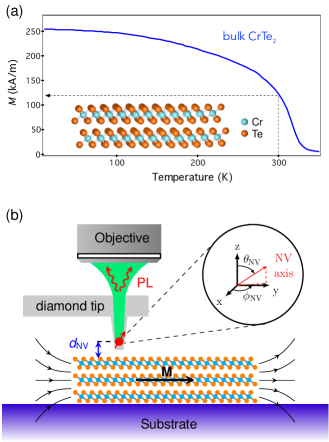
Magnetic imaging was performed with a scanning-NV magnetometer operating under ambient conditions Rondin et al. (2014). As sketched in Fig. 1(b), a single NV defect integrated into the tip of an atomic force microscope (AFM) was scanned above CrTe2 flakes to probe their stray magnetic fields. At each point of the scan, a confocal optical microscope placed above the tip was used to monitor the magnetic-field-dependent photoluminescence (PL) properties of the NV defect under green laser illumination. In this work, we employed a commercial diamond tip (Qnami, Quantilever MX) with a characteristic NV-to-sample distance nm, as measured through an independent calibration procedure Hingant et al. (2015). Two different magnetic imaging modes were used. In the limit of weak stray fields ( mT), quantitative magnetic field mapping was obtained by recording the Zeeman shift of the NV defect electron spin sublevels through optical detection of the electron spin resonance (ESR). This method relies on microwave driving of the NV spin transition combined with the detection of the spin-dependent PL intensity of the NV defect Gruber et al. (1997). For stronger magnetic fields ( mT), the scanning-NV magnetometer was rather used in all-optical, PL quenching mode Gross et al. (2018); Akhtar et al. (2019). In this case, localized regions of the sample producing large stray fields are simply revealed by an overall reduction of the PL signal induced by a mixing of the NV defect spin sublevels Tetienne et al. (2012). We note that the diameter of the scanning diamond tip is around nm in order to act as an efficient waveguide for the PL emission of the NV defect Maletinsky et al. (2012); Appel et al. (2016). As a result, such tips cannot provide precise topographic information of the sample. For the thinnest flakes, the topography was thus imaged by using conventional, sharp AFM tips.
For a ferromagnetic material, stray magnetic fields can be produced by magnetization patterns presenting a non-zero divergence . Considering a CrTe2 flake, this can occur (i) at the edges of the flake, (ii) at the location of non-collinear spin textures such as domain walls, and (iii) at the position of thickness steps on the flake. In this work, the magnetization is inferred from the measurement of the stray field produced at the edges of the flake [Fig. 1(b)]. Therefore, the analysis is made simpler for uniformly magnetized flakes with a homogeneous thickness. While uniform spin textures can be readily obtained by applying a bias magnetic field, obtaining thin CrTe2 flakes with a uniform thickness through mechanical exfoliation is currently achieved with a low probability. Consequently, variations in thickness must be carefully taken into account when analyzing the experimental results.
III Results and discussion
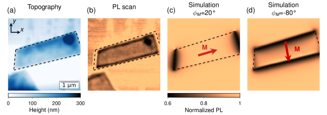
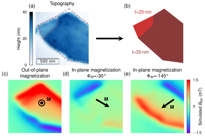
In a first experiment, we imaged a CrTe2 flake with a large thickness nm [Fig. 2(a)]. Considering the saturation magnetization of the bulk CrTe2 crystal, magnetic simulations predict stray field amplitudes larger than mT at a distance nm above the edges of the 150-nm-thick flake. The scanning-NV magnetometer was thus operated in the PL quenching mode for such a thick flake. Fig. 2(b) displays the resulting PL map. Several observations can be made. First, a quenching of the PL signal is observed when the NV defect is placed above the flake. This quenching effect, which is constant all over the flake, does not have a magnetic origin. It is linked to the metallic character of CrTe2 Buchler et al. (2005); Tisler et al. (2013). Second, a stronger PL quenching is obtained at the flake edges, as expected for a single ferromagnetic domain. We note that the additional quenching spot observed at the top-right edge of the flake results from the stray field produced by a large variation of the thickness [Fig. 2(a)]. Given the different sources of PL quenching involved in this experiment, quantitative estimates of the magnetization cannot be obtained. However, the analysis of the PL quenching distribution can be used to extract qualitative information about the orientation of the magnetization. To this end, simulations of the PL map were carried out considering only the effect of magnetic fields. The geometry of the flake used for the simulation was inferred from the AFM image simultaneously recorded with the NV microscope [Fig. 2(a)]. Assuming a uniform in-plane magnetization with an azimuthal angle in the plane, the stray field was first calculated at a distance above the flake. The resulting PL quenching map was then simulated by using the model of magnetic-field-dependent photodynamics of the NV defect described in Ref. Tetienne et al. (2012). Simulated PL maps obtained for two different orientations of the magnetization are shown in Figs. 2(c,d). In micron-sized flakes, shape anisotropy should favor a magnetization pointing along the long axis of the flake. Interestingly, the PL map simulated for such a magnetization direction disagrees with the experimental data [Fig. 2(c)], which instead suggest a magnetization pointing perpendicular to the long axis of the flake [Fig. 2(d)]. This result is a first indication of a non-negligible, in-plane magnetocrystalline anisotropy.
Thinner CrTe2 flakes, i.e. producing less stray field, were then studied through quantitative magnetic field imaging. To this end, a microwave excitation was applied through a copper microwire directly spanned on the sample surface and the Zeeman shift of the NV defect’s ESR frequency was recorded at each point of the scan. In the weak field regime, the ESR frequency is shifted linearly with the projection of the stray magnetic field along the NV defect quantization axis Rondin et al. (2014). This axis was precisely measured by applying a calibrated magnetic field Rondin et al. (2013), leading to the spherical angles and in the laboratory frame , as illustrated in Fig. 1(b). For these measurements, a bias field of was applied along the NV defect axis in order to infer the sign of the stray magnetic field Rondin et al. (2014). Furthermore, this bias field is strong enough to erase spin textures such as domain walls, given the weak coercitive field of CrTe2 flakes Purbawati et al. (2020).
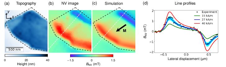
A map of recorded above a -nm thick CrTe2 flake is shown in Fig. 3(b). A stray magnetic field around mT is detected at two opposite edges of the flake. In principle, the underlying sample magnetization can be retrieved from such a quantitative magnetic field map by using reverse propagation methods with well-adjusted filters in Fourier-space Casola et al. (2018). Under several assumptions, this method can be quite robust for magnetic materials with out-of-plane magnetization Thiel et al. (2019); Broadway et al. (2020a); Sun et al. (2020b). For in plane magnets, however, the reconstruction procedure amplifies noise and is thus much less efficient Broadway et al. (2020b). As a result, the recorded magnetic field distribution was rather directly compared to magnetic calculations in order to extract quantitative information on the sample magnetization.
To obtain precise information on the geometry of the flake, the topography image was here measured with a sharp AFM tip [Fig. 3(a)]. The observed variations in thickness were included in the magnetic calculation (see Appendix A). Considering a uniformly magnetized flake with an azimuthal angle , the stray field was calculated at a distance above the flake and then projected along the NV quantization axis in order to simulate a map of . By comparing experimental data with magnetic maps simulated for different values of the angle , the orientation of the in-plane magnetization was first identified, leading to , i.e. pointing along the short axis of the flake [Fig. 3(c)]. Once again, this result suggests the presence of a non-negligible magnetocrystalline anisotropy, in agreement with recent works Purbawati et al. (2020). The norm of the magnetization vector was then estimated by fitting experimental line profiles with the result of the calculation, leading to kA/m [Fig. 3(d)]. We note that the stray field amplitude depends on several parameters including , , the flake thickness and the NV defect quantization axis . Any imprecisions on these parameters directly translate into uncertainties on the evaluation of the magnetization . A detailed analysis of uncertainties is provided in Appendix B.
The room-temperature magnetization measured in the exfoliated CrTe2 flake is almost five times smaller than the one obtained in the bulk crystal. This observation could be explained by a degradation of the sample surface through oxidation processes, leading to a thinner effective magnetic thickness. However, recent experiments relying on X-ray magnetic circular dichroism coupled to photoemission electron microscopy (XMCD-PEEM) have shown that oxidation is limited to the first outer layers of the CrTe2 flake Purbawati et al. (2020). Considering a -nm thick CrTe2 flake, surface oxidation can thus be safely neglected, and cannot explain the observed reduction of the magnetization. This effect is rather attributed to a decrease of the Curie temperature in exfoliated flakes, a phenomenon that has been observed in other vdW magnets such as Fe3GeTe2 below 5-10 nm thicknesses Fei et al. (2018); Tan et al. (2018), and in more traditional ferromagnetic thin films below few nanometers thicknesses Huang et al. (1994); Li and Baberschke (1992). The thickness marking the crossover from a thin film (2D-like) to a bulk magnetism (3D) is expected to be strongly material-dependent and cannot be predicted a priori in the case of CrTe2 Gibertini et al. (2019). However, for a -nm thick flake, bulk-like magnetism is a reasonable assumption and the magnetization’s amplitude should not be altered by the film thickness. In this thickness regime, the main parameter altering the magnetization’s amplitude is temperature, and how close or far it is from . The estimation of the reduction in Curie temperature was tentatively inferred by translating the Curie law measured for a bulk CrTe2 crystal [Fig. 1(a)] in order to reach kA/m at room temperature. This is achieved for a reduction of by K. This value is in line with a recent study, which estimates a Curie temperature around K for CrTe2 flakes with a few tens of nanometers thickness Sun et al. (2020a).
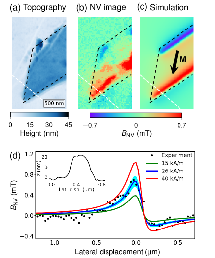
To support this finding, a similar analysis was performed for a 20-nm thick flake [Fig. 4(a)]. Here, a stray magnetic field is mainly detected along the bottom edge of the flake. On the opposite edge, the stray field distribution is quite inhomogeneous [Fig. 4(b)]. This observation is attributed to damages of the flake, which can be observed in the AFM image. It is difficult to describe the corresponding complex thickness variations, and hence to take them into account in the simulations. These height variations seem to correspond to several CrTe2 islands, whose very small sizes could make them more prone to oxidation than larger flakes, and which may exhibit random magnetization orientations. We hence disregarded the thickness variations in our structural model and the magnetic calculation was performed for a flake with uniform thickness, which is a good approximation for the bottom and left edges of the flake. A simulation of the stray field distribution for a magnetization with an azimuthal angle reproduces fairly well the experimental results [Fig. 4(c)] and a quantitative analysis of line profiles across the bottom edge of the flake leads to kA/m [Fig. 4(d)], a similar value to that obtained for the 35-nm thick flake. This observation indicates that the magnetization is not significantly modified for thicknesses lying in the few tens of nanometers range. A more in-depth analysis of the dependence of magnetization on thickness could not be carried out at this stage, given the very low probability to obtain thin CrTe2 flakes of homogeneous thickness through mechanical exfoliation.
IV Conclusion
To conclude, we have used quantitative magnetic imaging with a scanning-NV magnetometer to demonstrate that exfoliated CrTe2 flakes with thicknesses down to nm exhibit an in-plane ferromagnetic order at room temperature with a typical magnetization in the range of kA/m. These results make CrTe2 a unique system in the growing family of vdW ferromagnets, because it is the only material platform known to date which offers an intrinsic in-plane magnetization and a above room temperature in thin flakes. These properties might offer several opportunities for studying magnetic phase transition in 2D- systems Bedoya-Pinto et al. (2020) and to design spintronic devices based on vdW magnets. The next challenge will be to assess if the ferromagnetic order is preserved at room temperature in the few layers limit.
Acknowledgements
The authors warmly thank J. Vogel and M. Núñez-Regueiro for fruitful discussions. This research has received funding from the European Union H2020 Program under Grant Agreement No. 820394 (ASTERIQs), the DARPA TEE program, and the Flag-ERA JTC 2017 project MORE-MXenes. A.F. acknowledges financial support from the EU Horizon 2020 Research and Innovation program under the Marie Sklodowska-Curie Grant Agreement No. 846597 (DIMAF).
Appendix A: Magnetic field simulation
As indicated in the main text, thickness variations within the flake can result in a magnetization pattern with a non-zero divergence which produces a stray magnetic field. When possible, these variations were taken into account in the magnetic calculation. This is illustrated in Fig. 5(a,b), where the geometry of the flake used for the calculation includes a thickness step observed in the topography image. In Fig. 5(c-e), we show the magnetic field distributions produced at a distance nm for three different magnetization orientations of the flake. First considering an out-of-plane magnetization [Fig. 5(c)], the simulated magnetic field distribution does not agree with the experimental data shown in Fig. 3. This confirms that the magnetization in lying in the plane of the CrTe2 flake, i.e. perpendicular to the axis as obtained in the bulk crystal. Simulations performed for a uniform in-plane magnetization for two different values of the azimuthal angle in the plane are shown in Fig. 5(d,e). A comparison with experimental data allows the identification of the magnetization orientation.
Appendix B: Analysis of uncertainties
The norm of the magnetization is obtained by fitting line profiles of the measured stray field distribution with the result of the magnetic calculation [see Fig. 3(d)]. In this section, we analyze the uncertainty of this measurement by using the methodology described in Ref. Gross et al. (2017). The uncertainties result (i) from the fitting procedure itself and (ii) from those on the parameters which are all involved in the magnetic calculation. In the following, the parameters are expressed as , where denotes the nominal value of parameter and its standard error. These parameters are independently evaluated as follows:
-
The probe-to-sample distance is inferred through a calibration measurement, following the procedure described in Ref. Hingant et al. (2015), leading to nm.
-
The NV defect quantization axis is measured by recording the ESR frequency as a function of the amplitude and orientation of a calibrated magnetic field, leading to spherical angles in the laboratory frame of reference [see Fig. 1(b)].
-
The thickness of the CrTe2 flake is extracted from line profiles of the AFM image with an uncertainty of nm.
-
The azimuthal angle of the in-plane magnetization is obtained through the comparison between experimental data and simulated magnetic field maps.
We first evaluate the uncertainty of the fitting procedure. To this end, the line profile is fitted with the result of the magnetic calculation while fixing all the parameters to their nominal values , leading to kA/m. The relative uncertainty linked to the fitting procedure is therefore given by . We note that the intrinsic accuracy of the magnetic field measurement is in the range of T. The resulting uncertainty can be safely neglected.
In order to estimate the relative uncertainty introduced by each parameter , the fit was performed with one parameter fixed at , all the other parameters remaining fixed at their nominal values. The corresponding fit outcomes are denoted and . The relative uncertainty introduced by the errors on parameter is then finally defined as
| (1) |
This analysis was performed for each parameter . The cumulative uncertainty is finally given by
| (2) |
where all errors are assumed to be independent.
A summary of the uncertainties is given in Table I. We obtain kA/m for the flake shown in Fig. 3 and kA/m for the flake shown in Fig. 4.
(a) CrTe2 flake shown in Figure 3
| parameter | nominal value | uncertainty | |
|---|---|---|---|
| 80 nm | 10 nm | 8 | |
| 7 | |||
| 2 | |||
| nm | nm | 6 | |
| 5 | |||
| 14 | |||
(b) CrTe2 flake shown in Figure 4
| parameter | nominal value | uncertainty | |
|---|---|---|---|
| 80 nm | 10 nm | 8 | |
| 7 | |||
| 2 | |||
| nm | nm | 8 | |
| 12 | |||
| 17 | |||
References
- Kosterlitz and Thouless (1973) J. M. Kosterlitz and D. J. Thouless, J. Phys. C: Solid State Phys. 6, 1181 (1973).
- Li et al. (2019) H. Li, S. Ruan, and Y.-J. Zeng, Adv. Mater. 31, 1900065 (2019).
- Wang et al. (2020a) M.-C. Wang, C.-C. Huang, C.-H. Cheung, C.-Y. Chen, S. G. Tan, T.-W. Huang, Y. Zhao, Y. Zhao, G. Wu, Y.-P. Feng, H.-C. Wu, and C.-R. Chang, Annalen der Physik 532, 1900452 (2020a).
- Huang et al. (2017) B. Huang, G. Clark, E. Navarro-Moratalla, D. R. Klein, R. Cheng, K. L. Seyler, D. Zhong, E. Schmidgall, M. A. McGuire, D. H. Cobden, W. Yao, D. Xiao, P. Jarillo-Herrero, and X. Xu, Nature 546, 270 (2017).
- Gong et al. (2017) C. Gong, L. Li, Z. Li, H. Ji, A. Stern, Y. Xia, T. Cao, W. Bao, C. Wang, Y. Wang, Z. Q. Qiu, R. J. Cava, S. G. Louie, J. Xia, and X. Zhang, Nature 546, 265 (2017).
- Burch et al. (2018) K. S. Burch, D. Mandrus, and J.-G. Park, Nature 563, 47 (2018).
- Gong and Zang (2019) C. Gong and X. Zang, Science 363 (2019).
- Gibertini et al. (2019) M. Gibertini, M. Koperski, A. F. Morpurgo, and K. S. Novoselov, Nature Nanotechnology 14, 408 (2019).
- Liu et al. (2017) S. Liu, X. Yuan, Y. Zou, Y. Sheng, C. Huang, E. Zhang, J. Ling, Y. Liu, W. Wang, C. Zhang, J. Zou, K. Wang, and F. Xiu, npj 2D Materials and Applications 1, 30 (2017).
- Leon-Brito et al. (2016) N. Leon-Brito, E. D. Bauer, F. Ronning, J. D. Thompson, and R. Movshovich, Journal of Applied Physics 120, 083903 (2016).
- Fei et al. (2018) Z. Fei, B. Huang, P. Malinowski, W. Wang, T. Song, J. Sanchez, W. Yao, D. Xiao, X. Zhu, A. F. May, W. Wu, D. H. Cobden, J.-H. Chu, and X. Xu, Nature Materials 17, 778 (2018).
- Deng et al. (2018) Y. Deng, Y. Yu, Y. Song, J. Zhang, N. Z. Wang, Z. Sun, Y. Yi, Y. Z. Wu, S. Wu, J. Zhu, J. Wang, X. H. Chen, and Y. Zhang, Nature 563, 94 (2018).
- Weber et al. (2019) D. Weber, A. H. Trout, D. W. McComb, and J. E. Goldberger, Nano Lett. 19, 5031 (2019).
- Wang et al. (2020b) H. Wang, Y. Liu, P. Wu, W. Hou, Y. Jiang, X. Li, C. Pandey, D. Chen, Q. Yang, H. Wang, D. Wei, N. Lei, W. Kang, L. Wen, T. Nie, W. Zhao, and K. L. Wang, ACS Nano 14, 10045 (2020b).
- Li et al. (2018a) Q. Li, M. Yang, C. Gong, R. V. Chopdekar, A. T. N’Diaye, J. Turner, G. Chen, A. Scholl, P. Shafer, E. Arenholz, A. K. Schmid, S. Wang, K. Liu, N. Gao, A. S. Admasu, S.-W. Cheong, C. Hwang, J. Li, F. Wang, X. Zhang, and Z. Qiu, Nano Lett. 18, 5974 (2018a).
- May et al. (2019) A. F. May, D. Ovchinnikov, Q. Zheng, R. Hermann, S. Calder, B. Huang, Z. Fei, Y. Liu, X. Xu, and M. A. McGuire, ACS Nano 13, 4436 (2019).
- Seo et al. (2020) J. Seo, D. Y. Kim, E. S. An, K. Kim, G.-Y. Kim, S.-Y. Hwang, D. W. Kim, B. G. Jang, H. Kim, G. Eom, S. Y. Seo, R. Stania, M. Muntwiler, J. Lee, K. Watanabe, T. Taniguchi, Y. J. Jo, J. Lee, B. I. Min, M. H. Jo, H. W. Yeom, S.-Y. Choi, J. H. Shim, and J. S. Kim, Science Advances 6 (2020).
- Mallet et al. (2020) P. Mallet, F. Chiapello, H. Okuno, H. Boukari, M. Jamet, and J.-Y. Veuillen, Phys. Rev. Lett. 125, 036802 (2020).
- Yun et al. (2020) S. J. Yun, D. L. Duong, D. M. Ha, K. Singh, T. L. Phan, W. Choi, Y.-M. Kim, and Y. H. Lee, Advanced Science 7, 1903076 (2020).
- F. et al. (2020) Z. F., B. Zheng, A. Sebastian, H. Olson, M. Liu, K. Fujisawa, Y. T. H. Pham, V. Ortiz Jimenez, V. Kalappattil, L. Miao, T. Zhang, R. Pendurthi, Y. Lei, A. L. Elias, Y. Wang, N. Alem, P. E. Hopkins, S. Das, V. H. Crespi, M.-H. Phan, and M. Terrones, arXiv:2005.01965 (2020).
- Bonilla et al. (2018) M. Bonilla, S. Kolekar, Y. Ma, H. C. Diaz, V. Kalappattil, R. Das, T. Eggers, H. R. Gutierrez, M.-H. Phan, and M. Batzill, Nature Nanotechnology 13, 289 (2018).
- O’Hara et al. (2018) D. J. O’Hara, T. Zhu, A. H. Trout, A. S. Ahmed, Y. K. Luo, C. H. Lee, M. R. Brenner, S. Rajan, J. A. Gupta, D. W. McComb, and R. K. Kawakami, Nano Letters 18, 3125 (2018).
- Li et al. (2018b) J. Li, B. Zhao, P. Chen, R. Wu, B. Li, Q. Xia, G. Guo, J. Luo, K. Zang, Z. Zhang, H. Ma, G. Sun, X. Duan, and X. Duan, Advanced Materials 30, 1801043 (2018b).
- Feng et al. (2019) J. Feng, D. Biswas, A. Rajan, M. D. Watson, F. Mazzola, O. J. Clark, K. Underwood, I. Markovic, M. McLaren, A. Hunter, D. M. Burn, L. B. Duffy, S. Barua, G. Balakrishnan, F. Bertran, P. Le Fevre, T. K. Kim, G. van der Laan, T. Hesjedal, P. Wahl, and P. D. C. King, Nano Lett. 18, 4493 (2019).
- Wong et al. (2019) P. K. J. Wong, W. Zhang, F. Bussolotti, X. Yin, T. S. Herng, L. Zhang, Y. L. Huang, G. Vinai, S. Krishnamurthi, D. W. Bukhvalov, Y. J. Zheng, R. Chua, A. T. N’Diaye, S. A. Morton, C.-Y. Yang, K.-H. Ou Yang, P. Torelli, W. Chen, K. E. J. Goh, J. Ding, M.-T. Lin, G. Brocks, M. P. de Jong, A. H. Castro Neto, and A. T. S. Wee, Advanced Materials 31, 1901185 (2019).
- Freitas et al. (2015) D. C. Freitas, R. Weht, A. Sulpice, G. Remenyi, P. Strobel, F. Gay, J. Marcus, and M. Núñez-Regueiro, Journal of Physics: Condensed Matter 27, 176002 (2015).
- Sun et al. (2020a) X. Sun, W. Li, X. Wang, Q. Sui, T. Zhang, Z. Wang, L. Liu, D. Li, S. Feng, S. Zhong, H. Wang, V. Bouchiat, M. Nunez Regueiro, N. Rougemaille, J. Coraux, A. Purbawati, A. Hadj-Azzem, Z. Wang, B. Dong, X. Wu, T. Yang, G. Yu, B. Wang, Z. Han, X. Han, and Z. Zhang, Nano Research (2020a).
- Purbawati et al. (2020) A. Purbawati, J. Coraux, J. Vogel, A. Hadj-Azzem, N. Wu, N. Bendiab, D. Jegouso, J. Renard, L. Marty, V. Bouchiat, A. Sulpice, L. Aballe, M. Foerster, F. Genuzio, A. Locatelli, T. O. Menteş, Z. V. Han, X. Sun, M. Núñez-Regueiro, and N. Rougemaille, ACS Appl. Mater. Interfaces 12, 30702 (2020).
- Balasubramanian et al. (2008) G. Balasubramanian, I. Y. Chan, R. Kolesov, M. Al-Hmoud, J. Tisler, C. Shin, C. Kim, A. Wojcik, P. R. Hemmer, A. Krueger, T. Hanke, A. Leitenstorfer, R. Bratschitsch, F. Jelezko, and J. Wrachtrup, Nature 455, 648 (2008).
- Maze et al. (2008) J. R. Maze, P. L. Stanwix, J. S. Hodges, S. Hong, J. M. Taylor, P. Cappellaro, L. Jiang, M. V. G. Dutt, E. Togan, A. S. Zibrov, A. Yacoby, R. L. Walsworth, and M. D. Lukin, Nature 455, 644 (2008).
- Rondin et al. (2014) L. Rondin, J.-P. Tetienne, T. Hingant, J.-F. Roch, P. Maletinsky, and V. Jacques, Reports on Progress in Physics 77, 056503 (2014).
- Casola et al. (2018) F. Casola, T. van der Sar, and A. Yacoby, Nature Reviews Materials 3, 17088 (2018).
- Tetienne et al. (2015) J.-P. Tetienne, T. Hingant, L. J. Martinez, S. Rohart, A. Thiaville, L. H. Diez, K. Garcia, J.-P. Adam, J.-V. Kim, J.-F. Roch, I. M. Miron, G. Gaudin, L. Vila, B. Ocker, D. Ravelosona, and V. Jacques, Nature Communications 6, 6733 (2015).
- Dovzhenko et al. (2018) Y. Dovzhenko, F. Casola, S. Schlotter, T. X. Zhou, F. Buttner, R. L. Walsworth, G. S. D. Beach, and A. Yacoby, Nature Communications 9, 2712 (2018).
- Chauleau et al. (2020) J.-Y. Chauleau, T. Chirac, S. Fusil, V. Garcia, W. Akhtar, J. Tranchida, P. Thibaudeau, I. Gross, C. Blouzon, A. Finco, M. Bibes, B. Dkhil, D. D. Khalyavin, P. Manuel, V. Jacques, N. Jaouen, and M. Viret, Nature Materials 19, 386 (2020).
- Ku et al. (2020) M. J. H. Ku, T. X. Zhou, Q. Li, Y. J. Shin, J. K. Shi, C. Burch, L. E. Anderson, A. T. Pierce, Y. Xie, A. Hamo, U. Vool, H. Zhang, F. Casola, T. Taniguchi, K. Watanabe, M. M. Fogler, P. Kim, A. Yacoby, and R. L. Walsworth, Nature 583, 537 (2020).
- Thiel et al. (2019) L. Thiel, Z. Wang, M. A. Tschudin, D. Rohner, I. Gutiérrez-Lezama, N. Ubrig, M. Gibertini, E. Giannini, A. F. Morpurgo, and P. Maletinsky, Science 364, 973 (2019).
- Broadway et al. (2020a) D. A. Broadway, S. C. Scholten, C. Tan, N. Dontschuk, S. E. Lillie, B. C. Johnson, G. Zheng, Z. Wang, A. R. Oganov, S. Tian, C. Li, H. Lei, L. Wang, L. C. L. Hollenberg, and J.-P. Tetienne, Adv. Mater. n/a, 2003314 (2020a).
- Sun et al. (2020b) Q.-C. Sun, T. Song, E. Anderson, T. Shalomayeva, J. Förster, A. Brunner, T. Taniguchi, K. Watanabe, J. Gräfe, R. Stöhr, X. Xu, and J. Wrachtrup, arXiv:2009.13440 (2020b).
- Hingant et al. (2015) T. Hingant, J.-P. Tetienne, L. J. Martínez, K. Garcia, D. Ravelosona, J.-F. Roch, and V. Jacques, Physical Review Applied 4, 014003 (2015).
- Gruber et al. (1997) A. Gruber, A. Dräbenstedt, C. Tietz, L. Fleury, J. Wrachtrup, and C. V. Borczyskowski, Science 276, 2012 (1997).
- Gross et al. (2018) I. Gross, W. Akhtar, A. Hrabec, J. Sampaio, L. J. Martínez, S. Chouaieb, B. J. Shields, P. Maletinsky, A. Thiaville, S. Rohart, and V. Jacques, Phys. Rev. Materials 2, 024406 (2018).
- Akhtar et al. (2019) W. Akhtar, A. Hrabec, S. Chouaieb, A. Haykal, I. Gross, M. Belmeguenai, M. Gabor, B. Shields, P. Maletinsky, A. Thiaville, S. Rohart, and V. Jacques, Phys. Rev. Applied 11, 034066 (2019).
- Tetienne et al. (2012) J.-P. Tetienne, L. Rondin, P. Spinicelli, M. Chipaux, T. Debuisschert, J.-F. Roch, and V. Jacques, New Journal of Physics 14, 103033 (2012).
- Maletinsky et al. (2012) P. Maletinsky, S. Hong, M. S. Grinolds, B. Hausmann, M. D. Lukin, R. L. Walsworth, M. Loncar, and A. Yacoby, Nature Nanotechnology 7, 320 (2012).
- Appel et al. (2016) P. Appel, E. Neu, M. Ganzhorn, A. Barfuss, M. Batzer, M. Gratz, A. Tschöpe, and P. Maletinsky, Review of Scientific Instruments 87, 063703 (2016).
- Buchler et al. (2005) B. C. Buchler, T. Kalkbrenner, C. Hettich, and V. Sandoghdar, Phys. Rev. Lett. 95, 063003 (2005).
- Tisler et al. (2013) J. Tisler, T. Oeckinghaus, R. J. Stöhr, R. Kolesov, R. Reuter, F. Reinhard, and J. Wrachtrup, Nano Lett. 13, 3152 (2013).
- Rondin et al. (2013) L. Rondin, J.-P. Tetienne, S. Rohart, a. Thiaville, T. Hingant, P. Spinicelli, J.-F. Roch, and V. Jacques, Nat. Commun. 4, 2279 (2013).
- Broadway et al. (2020b) D. A. Broadway, S. E. Lillie, S. C. Scholten, D. Rohner, N. Dontschuk, P. Maletinsky, J.-P. Tetienne, and L. C. L. Hollenberg, Phys. Rev. Applied 14, 024076 (2020b).
- Tan et al. (2018) C. Tan, J. Lee, S.-G. Jung, T. Park, S. Albarakati, J. Partridge, M. R. Field, D. G. McCulloch, L. Wang, and C. Lee, Nature Communications 9, 1554 (2018).
- Huang et al. (1994) F. Huang, M. T. Kief, G. J. Mankey, and R. F. Willis, Phys. Rev. B 49, 3962 (1994).
- Li and Baberschke (1992) Y. Li and K. Baberschke, Phys. Rev. Lett. 68, 1208 (1992).
- Bedoya-Pinto et al. (2020) A. Bedoya-Pinto, J.-R. Ji, A. Pandeya, P. Gargiani, M. Valvidares, P. Sessi, F. Radu, K. Chang, and S. Parkin, arXiv:2006.07605 (2020).
- Gross et al. (2017) I. Gross, W. Akhtar, V. Garcia, L. J. Martínez, S. Chouaieb, K. Garcia, C. Carrétéro, A. Barthélémy, P. Appel, P. Maletinsky, J.-V. Kim, J. Y. Chauleau, N. Jaouen, M. Viret, M. Bibes, S. Fusil, and V. Jacques, Nature 549, 252 (2017).