Hard wall edge confinement in 2D topological insulators and the energy of the Dirac Point
Abstract
In 2D topological insulators (TIs) based on semiconductor quantum wells such as HgTe/CdTe or InAs/GaSb/AlSb, spin polarized edge states have been predicted with a massless Dirac like dispersion. In a hard wall treatment based on the BHZ Hamiltonian and open boundary conditions (OBCs), the wave function is weakly confined near the edge, with which it makes no contact. In contrast, standard boundary conditions for the wave function and its derivative (SBCs) lead to strong confinement with a peak amplitude at the edge. Unfortunately, weak confinement exhibits unphysical behavior related to a spurious gap solution that is included in the OBC wave function. This is confirmed by the gap solutions of the parent multiband Hamiltonian from which the smaller Hamiltonian is derived, which exhibit physical behavior and do not satisfy OBCs. Unlike OBCs or other approaches based on phenomenological boundary conditions, SBCs treat the wall explicitly. Using a basis of empty crystal free electron states for the vacuum with the same symmetry as the TI states, it is shown that a large wall band gap overlapping that of the TI can only be achieved by including a thin passivation layer. For passivation materials such as silicon dioxide where the mid gap energy is nearly degenerate with that of the TI, the Dirac point is very close to mid gap and virtually independent of the TI band asymmetry. The treatment also demonstrates that a significant shift of the dispersion may be introduced by interface band mixing. The shift is largest at the Dirac point and decreases monotonically with edge state wave vector, vanishing when the edge states merge with the bulk band edges.
pacs:
73.21.-b, 73.23.-b, 73.61.Ey, 73.61.Ga
I INTRODUCTION
Surface states occur in many areas of condensed matter physics, often when some material parameter changes sign across a boundary. Two classic examples are surface plasmons and surface optical phonons, where a sign reversal of the dielectric function leads to edge confinement with an amplitude that decays away from the edge, both into the material and into the surroundings.(Yu and Cardona, 1996; Ritchie, 1957; Pitarke et al., 2007; Fuchs and Kliewer, 1965; Sood et al., 1985) More recently, electronic edge states have been discovered in topological insulators (TIs), where a change in sign of the band gap parameter reverses the ordering of even and odd parity crystal periodic basis functions.(Qi and Zhang, 2010) These edge states also have the unique property that their direction of motion depends on the electron spin, leading to unusual phenomena such as dissipationless ballistic transport and the quantum spin Hall effect.(Bernevig et al., 2006; König et al., 2008) Their experimental observation, however, remains a challenge and in some cases more advanced surface passivation techniques may be needed, in order to eliminate parallel conduction paths through trivial edge states due, for example, to unsatisfied dangling bonds.(Nichele et al., 2016)
A popular treatment for the spin polarized edge states in TIs is based on the theory, where useful results can be obtained with the simple four band BHZ Hamiltonian based on blocks for each spin direction.(Bernevig et al., 2006) Each block is associated with a Chern number whose value on each side of the boundary can be related to the number of spin-polarized edge states. At a hard wall, the nature of the edge state confinement can depend strongly on the boundary conditions used. Standard boundary conditions for the wave function and its derivative (SBCs) and other related approaches, can lead to strong confinement, where the wave function has a peak amplitude at the edge, similar to the classic surface states described above.Klipstein (2015); *KlipErratum2016; Tkachov and Hankiewicz (2010, 2013); Medhi and Shenoy (2012) On the other hand, open boundary conditions (OBCs) lead to weak confinement, where the amplitude is zero at the edge and only reaches a peak typically 10-100 Å away.(König et al., 2008; Zhou et al., 2008; Essert, 2015)While deep quantum well (QW) states also have negligible amplitude at the edge of the well, the bound state vanishes when one of the barriers is removed and this should not be confused with true edge confinement. Of these methods, the OBC approach is by far the most popular because it apparently avoids any explicit treatment of the wall.(Qi et al., 2006; König et al., 2007; Dai et al., 2008; König et al., 2008; Liu et al., 2008; Zhou et al., 2008; Linder et al., 2009; Liu et al., 2010; Lu et al., 2010; Shan et al., 2010; Sonin, 2010; Murakami, 2011; Shen et al., 2011; Wada et al., 2011; Michetti et al., 2012a, b; Takagaki, 2012; Cano-Corte’s et al., 2013; Hohenadler and Assaad, 2013; Sengupta et al., 2013; Wang et al., 2014; Xu et al., 2014; Essert, 2015; Enaldiev et al., 2015; Durnev and Tarasenko, 2016; Entin et al., 2017; Candido et al., 2020; Gioia et al., 2018; Durnev and Tarasenko, 2019; Gioia et al., 2019; Böttcher et al., 2020; Durnev, 2020) Notwithstanding the greater simplicity of OBCs, this author has previously argued that the spin polarized edge states in TIs cannot have zero amplitude at the edge, and in this respect they are no different from their classic plasmon or phonon counterparts. The weakly confined wave function in the OBC treatment arises from a mathematically correct but physically spurious solution of the four band BHZ Hamiltonian for each spin direction, which not only gives an unphysical wave function but also leads to other unphysical properties. The aim of the present work is to provide further evidence for this point of view, based on an eight band treatment. It is shown that edge states are not possible in the eight band model using OBCs, while the four band and eight band results correspond very well when SBCs are used. In contrast to some alternatives to OBCs, which are phenomenological in nature and do not consider the wall explicitly,(Medhi and Shenoy, 2012; Enaldiev et al., 2015; Entin et al., 2017) SBCs provide a realistic physical picture on both sides of the boundary. They can also give a physical edge dispersion whose Dirac point is close to mid gap, even when band structure asymmetry would cause the Dirac point to be near a bulk band edge in the four band OBC treatment.
In most cubic semiconductors, one of the crystal periodic basis functions of the BHZ Hamiltonian is based on antibonding s-orbitals, while the other is based on bonding p-orbitals, corresponding to the conduction and valence bands, respectively. In two dimensional TIs, usually based on semiconductor QWs such as HgTe/CdTe or InAs/GaSb/AlSb, their order can be reversed by increasing the QW width. Spin polarized edge states are then predicted according to the change in Chern number at the boundary with the wall or other semiconductor material.(Kane, 2013) For a TI with symmetrical bands, the spin up Hamiltonian can be written: and the Chern number is given by , where is the semiconductor band gap, is related to the band effective mass, and is the in-plane wave-vector.(Shen et al., 2011) The symmetrical operator ordering used in the quadratic term has been justified in Ref. Klipstein, 2010. For a boundary between a TI material with , and a wall with - and -parameter values, , , the change in Chern number is , supporting a single spin-polarized edge state. If the sign of is reversed, and two edge states are predicted. Examples of both types will be discussed in this work.
 |
 |
| (a) | (b) |
 |
|
| (c) | |
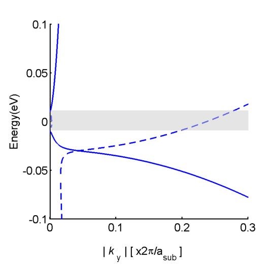
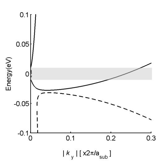
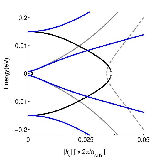
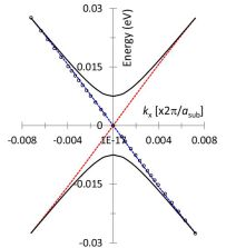
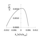
Band asymmetry can be incorporated into the 2 x 2 spin up Hamiltonian by adding an additional term proportional to the identity matrix, , yielding , and parameter values can be found, usually empirically, which provide a good description of the small wave vector states near the band edges of most semiconductor materials. There are also solutions in the band gap energy range, . Considering the dispersion in the -direction (), the “middle states” have a small imaginary wave vector, , and describe tunneling, for example when the semiconductor is used as a thin barrier material. The “wing states” , on the other hand, have a wave vector, , that is imaginary or real, depending on whether or , respectively. When the difference between and is small, the decay parameter at zero energy is given by the simple formula: , showing that its magnitude depends on the difference, and that the state is only evanescent when D < B. This is demonstrated in Fig. 1, which compares two TI Hamiltonians with , , and , and where extended and evanescent states are depicted as solid and dashed lines, respectively. Wave vectors are plotted in units of , where (the value of the GaSb cubic lattice parameter). The blue plot in Fig. 1(a) is for , while the black plot in Fig. 1(b) is for . The same color scheme is used in Fig. 1(c), where the results for both -values are superimposed in the small wave vector region. The switch between large imaginary and real wing wave vectors of the same magnitude shows clearly in the shaded band gap region of Figs. 1(a) and 1(b), occurring when the crossing of extended and evanescent states below the band gap changes to an anti-crossing. In contrast, the middle states with small imaginary wave vector in Fig. 1(c) are indistinguishable for the two cases and totally insensitive to the increase in . The spurious nature of the wing states was first discussed by White and Sham(White and Sham, 1981), and later by Schuurmans and t’Hooft (Schuurmans and t’Hooft, 1985). Both the extended and evanescent solutions do not correspond to any plausible dispersion and are obviously unphysical.111A physical dispersion must be evanescent in the band gap, starting and finishing at a band edge. As discussed in these same references, and demonstrated explicitly in Sec. II, the wing solutions arise because the number of basis states is too small. The effect of remote states which have been omitted from the Hamiltonian is incorporated in the quadratic terms (proportional to and ) using perturbation theory, and this always leads to a spurious solution. Moreover, since the range of real or imaginary wave vectors must then be limited to magnitudes, , where the perturbation terms are less than the typical band energy, the spurious solution is usually found to lie well beyond this limit (see Sec. III). For the example in Fig. 1, the valid range corresponds to , which is the range plotted for the middle solution in Fig. 1(c). The valid range thus includes the middle solution but is about 50 times smaller than the band gap wave vectors of the wing solutions in Figs. 1(a) and 1(b).
The behavior shown in Fig. 1 is quite general, as can be seen from the simple formula given above for , which always gives a switch been real and imaginary wing wave vectors when D = B, regardless of the sign of M, or the magnitude of B and D. When B and D are small, the wing solution can lie far outside the Brillouin zone, while the middle solution, , is very insensitive to their values. The eigenvectors for the and solutions at a given energy are usually different. However, in a TI material with M < 0 and D < B, it turns out that they are identical at energy (see Sec. III), which is just below the conduction band edge in the example of Fig. 1(a).(Zhou et al., 2008) This has led to the common but unfortunate practice of adopting OBC boundary conditions, where both solutions are treated completely seriously and combined into a single wave function with an envelope of the form, , so that the amplitude is zero at the sample boundary, which is assumed to be a hard wall at . Although this would be correct if yielded only physical solutions, the inclusion of the spurious solution in the wave function leads to several problematic results, which have been discussed previously and which will be elaborated below. In order to clarify the matter, the results of the two band spin up model are compared in Sec. II, with a multiband spin up model where the remote states are included explicitly. When at least four bands are included, both small and large imaginary wave vector solutions still appear, but in this case the latter is a physical tunneling state containing large eigenvector amplitudes from the additional bands. On the other hand, the small imaginary wave vector solution has almost zero amplitudes from these bands (as for the two band, spin up model), so it is now impossible to combine the two solutions and satisfy OBCs. Since the two band spin up model is simply a perturbation approximation of the multiband spin up model, this confirms that something is wrong with the OBC approach.
The problem with OBCs has been highlighted previously by the author and an alternative approach was proposed for the two band spin up model, based on SBC boundary conditions.(Klipstein, 2015, 2018) Although SBCs treatments have been reported by other workers, they are generally based on a soft wall and evolve into OBCs when the wall potential increases, because the wave function still includes the spurious solution(Michetti et al., 2012b; Durnev, 2020). The SBC approach proposed by the author is for a hard wall and does not include the spurious and physical solutions in the same wave function. It was shown in previous work that two exponential edge solutions can be found when (and ) is (are) negative, consistent with when . One of these involves only solutions in the TI and wall, and the other only solutions. The former yields a simple edge state dispersion in the useful limit, , and , close to , which merges smoothly with the bulk band edges, while the latter shows unphysical merging behavior and is rejected as spurious. It will be shown in Sec. II that these results are entirely consistent with the SBC multiband spin up model, which also puts the Dirac point close to mid gap. When (and ) is (are) positive a single, non-exponential solution exists, again consistent with both models.
In previous work based on the two band spin up model, the edge dispersion was obtained by solving a characteristic equation numerically, for both strongly hybridized HgTe/CdTe and weakly hybridized InAs/GaSb/AlSb QWs.(Klipstein, 2018) In Sec. III of this work, an analytical solution is obtained for the dispersion, which provides a simple expression for the energy of the Dirac point. The dependence of the Dirac point on the wall hybridization parameters is then compared for the two and four band spin up models in Sec. IV. Although the wall hybridization parameters are found to have a relatively small effect, a suitable model of the wall region is lacking. Therefore, in Sec. V, an approach is proposed for a consistent treatment. This approach yields a wall hybridization parameter in the two band spin up model that is fairly similar to that in the TI material, and much smaller than the free electron Dirac value, which was previously suggested as a possibility. It also highlights the importance of an edge passivation material and introduces interface band mixing terms which may cause a significant additional shift of the Dirac point. In Sec. VI, conclusions are summarized. Even though this work is focused primarily on the physical nature of the wave function confinement and its influence on the energy of the Dirac point, a multiband spin up treatment of the full edge dispersion is presented in Appendix A, where it is shown to be quite consistent with the SBC two band spin up approach.
II MULTIBAND MODEL OF DIRAC POINT
II.1 Hamiltonian
In 1955, Luttinger and Kohn derived the theory in Fourier space and showed how it could be used to treat the potential of an impurity atom in a bulk crystal.(Luttinger and Kohn, 1955) This was extended by Volkov and Takhtamirov in the 1990s, who used the same approach to treat semiconductor superlattices.(Volkov and Takhtamirov, 1997; Takhtamirov and Volkov, 1997, 1999) When transformed into real space and with a few basic assumptions, their Hamiltonian can be written:(Klipstein, 2010)
| (1) |
where is the band edge of the zone center basis state , is the envelope function which only contains Fourier components in the first Brillouin zone, and is a momentum matrix element between crystal periodic basis states and . For an infinite bulk material, is a plane wave. The term represents additional terms introduced when the crystal potential is modulated along the y-direction, for instance at a boundary between two different materials.(Volkov and Takhtamirov, 1997; Takhtamirov and Volkov, 1997, 1999; Klipstein, 2010) This term is not included in the present bulk treatment, but is discussed further in Sec. V.
Eq. (1) can be written in matrix form with elements, , and for a bulk material with , it is essentially an exact description of the crystal if enough basis states are included. For example, in their seminal work of 1966, Cardona and Pollak were able to model the whole Brillouin zones of silicon and germanium with 15 zone center basis states.(Cardona and Pollak, 1966) However, in cases where only a small local region of the Brillouin zone is of interest, it is possible to eliminate a large number of the remote states using perturbation theory, leaving only those states in the local energy range. The Bir and Pikus expression for the local Hamiltonian, can be written up to second order as(Bir and Pikus, 1974):
| (2) |
in which the local states are , , etc., the remote states are , , etc., and is an off-diagonal matrix element of where . This reduces the size of the Hamiltonian, but introduces additional k-quadratic matrix elements into the Hamiltonian of local states, .
The model Hamiltonian for a 2D quantum well, , discussed in Sec. I, is thus derived from a larger number of basis states, using Eq. (2). As a simple example, consider the following unperturbed spin up Hamiltonian based on Eq. (1), with a basis, :
| (3) |
where , , and . The states and are anti-bonding s- and bonding p-states discussed in Sec. I. These interact with remote states and , at energies, and , respectively.222If and are interchanged in the Q-terms of Eq. (3), corresponding to a change in symmetry of the remote states, there is no change to the energy of the Dirac point based on the present multiband model, and the edge state dispersions are essentially the same as those derived in Appendix A.
Because is quite small, the quadratic term in the first line of Eq. (3) will be ignored. Moreover, its inclusion would lead to non-exponential hard wall edge state solutions which are not considered in this work. The effect of including this term will be discussed further at the end of Sec. V. Using the perturbation expression in Eq. (2), is then reduced to where:
| (4a) | |||
| (4b) |
If more bands are included in the multiband Hamiltonian of Eq. (3) that interact with bands and , there will simply be an additional term for each band in the expressions for B and D. This procedure is analogous to that used to derive the BHZ Hamiltonian in the supplementary material of Ref. Bernevig et al., 2006, where B and D were calculated from the Luttinger parameters. The Luttinger parameters depend on interactions with remote states, which can be expressed in a similar form to Eq. (4b).(Lawaetz, 1971)
Eq. (4b) shows that the size of the reciprocal mass terms, B and D, in is determined by the interaction with the remote states, and that have been eliminated. If these states are removed to infinity, i.e. , the reciprocal mass terms are reduced to zero. This highlights a first problem with OBCs. As discussed in Sec. I, the Dirac point of the edge states in the OBC model occurs at . Thus for a given ratio, , the shift of the Dirac point from mid gap remains fixed, even when D and B become vanishingly small. In fact, the whole dispersion remains fixed (see Sec. III). This kind of behavior is not physical, because remote states which are far away in energy cause the same shift as when they are much closer.
 |
| (a) |
 |
| (b) |
II.2 Failure of OBC’s
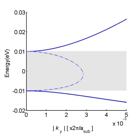
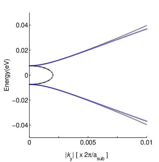
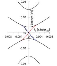
Fig. 2 shows the extended and evanescent states, in blue and black, respectively, calculated from with = 0, for the case of a symmetric inverted band gap where , = and . In addition to physical tunneling states connecting bands and , as in the two band spin up model discussed in Sec. I, there are now physical tunneling states also connecting bands and . Superimposed in gray are the solutions of with the same M and A values, and with , , calculated from the M, Q and -values using Eq. (4b). It can be seen in Fig. 2(a) that the two dispersions correspond very well for the middle states and for the conduction and valence band edges out to , which is consistent with the valid range of wave vectors for the two band spin up model, , discussed in Sec. I. However Fig. 2(b) shows that the two dispersions are completely different in the vicinity of the wing states. This highlights the spurious nature of the wing dispersion of , even when D = 0. The two models only agree near imaginary wave vector, , demonstrating that the spurious branch is a phantom like dispersion associated with bands and that have been eliminated. It cannot merge with these band edges as in the multiband model, because they are no longer there, so adopts a meaningless trajectory towards the Brillouin zone boundary.
The zero energy eigenvectors of the middle and wing solutions of the two band spin up model are both , which enables their combination into an OBC wave function at the Dirac point, as discussed in Sec. I. Such combination is unfortunate, because a proper description of the wing solution should contain a significant amplitude from the absent states, and . This can be seen in the zero energy eigenvectors of the multiband spin up model, which are given in the first two columns of Table 2 for the parameters used in Fig. 2, namely and . These eigenvectors contain contributions from the relevant bands and represent the different physical nature of the two states correctly. However, in consequence, they can no longer be combined into a wave function which satisfies OBCs, showing that there is a fundamental problem with the OBC approach.
II.3 Edge states using SBC’s
In the rest of this work the hard wall SBC approach, described in Sec. I and introduced by the author in an earlier four band treatment,(Klipstein, 2015, 2016, 2018) is discussed within the context of the multiband model. The wall region is treated explicitly, because the edge state wave functions decay on both sides of the boundary. Since the eigenvectors of the middle and wing solutions are different in the multiband model, it is necessary to ensure continuity of the two vector components independently. This is entirely consistent with the separation of the middle and wing solutions in the previously reported four band treatment, and leads to similar results. In contrast to the OBC treatment, the Dirac point always remains very close to mid gap, even when the semiconductor band dispersions become asymmetric. It is assumed that the wall has a large fundamental band gap, , that is symmetrically disposed about that of the semiconductor. How this is realized in practice, and the consequences of when this is not the case are discussed in Sec. V. It turns out that there are only exponential edge state solutions when the wall parameters have a certain relationship with those in the semiconductor. Since the number of eigenvalues is conserved when some system parameter is varied, solutions exist for other combinations of wall and semiconductor parameters but they are no longer exponential. An exponential solution exists, however, when and the wall band gap is effectively infinite, so this is the limit that is used in both models. It can be reached by a trajectory in parameter space that involves only exponential solutions (as in this work) or otherwise. At the same time, a band gap that is truly infinite results in an unphysically rapid decay of the wavefunction in the wall region. Typical band gap values for the wall based on real physical systems are discussed in Sec. V.
Two specific cases are now treated for the multiband spin up model. The simplest case is for a symmetric semiconductor band structure. Next, band asymmetry is included. In both treatments, the same values are used for the electron-hole hybridization parameters in the semiconductor and the wall, and it is shown that this always puts the Dirac point exactly at mid gap, even when the band structure is asymmetric. The multiband spin up treatment where these parameters are different is reserved to Sec. IV, after the corresponding results for the two band spin up model are derived in Sec. III.
| Decay Parameter | Eigenvector |
|---|---|
Table 1 gives expressions for the pair of zero energy decay parameters, , in the y-direction and their corresponding eigenvectors, , of the symmetric multiband spin up model, expressed in terms of the following quantities:
| (5a) | |||
| (5b) | |||
| (5c) |
| Parameter | Semicond. | Wall (-ve ) | Wall (+ve ) | |||
| 4 band | ||||||
| (eV Å) | 3.83 | 3.83 | 3.83 | |||
| (eV Å) | 3.83 | 3.83 | 3.83 | |||
| -20 | -20 | 50 | ||||
| 0.0020 | 0.0360 | -53.48 | -959.7 | -49.68 | -2582.6 | |
| a | i0.037 | i0.486 | i0.037 | i0.486 | -i0.014 | i0.505 |
| b | 0.706 | 0.513 | 0.706 | 0.513 | 0.707 | 0.495 |
| c | -0.706 | -0.513 | -0.706 | -0.513 | -0.707 | 0.495 |
| d | i0.037 | i0.486 | i0.037 | i0.486 | -i0.014 | -i0.505 |
| 2 band | ||||||
| 102.9 | -0.00386 | 0.00144 | ||||
| 0.0020 | 0.0341 | -53.65 | -908.9 | -49.7 | -2633.3 | |
| a | 0.707 | 0.707 | 0.707 | 0.707 | 0.707 | 0.707 |
| b | -0.707 | -0.707 | -0.707 | -0.707 | -0.707 | 0.707 |
The parameter, , has a value of +1 for the semiconductor and -1 for the wall. In contrast to the two band spin up model, where boundary conditions exist for both the wave function and its derivative, the only boundary condition in the multiband spin up model is the continuity of the wave function, because is linear in . For an edge at y = 0, this means that edge solutions must have the same eigenvectors on each side of the boundary. Since the zero energy eigenvectors in Table 1 only depend on the ratio of the two band gap parameters, M and , it is always possible to match the solutions with small or large decay parameters, independently, for a given A and Q, provided the band gap parameters in the semiconductor and wall have the same ratio. Examples are shown in Table 2 for the same parameters used in Fig. 2, with , where and are the band gaps between the inner and outer bands, respectively, in the wall material. Note that is negative, because M and have opposite signs. In the Table, the eigenvectors for the small decay parameter (large decay parameter) on each side of the boundary are written with a small (large) typeface, so that the correspondence between the eigenvectors in each group can be seen clearly. Inserting into Eq. (4b) gives for the two band spin up model. It was shown in previous work that for this value of there are two exponential edge states corresponding to the same matching of solutions with either a small or a large decay parameter, respectively.(Klipstein, 2015, 2018) Both models thus obey the same condition for the two exponential edge solutions. Moreover, or as , both of which are realistic descriptions of a hard wall.
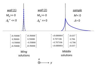
Positive solutions (corresponding to positive in the two band spin up model) are shown in the last column of Table 2, where there is only fairly close agreement between eigenvectors for the small decay parameters on each side of the boundary. The values for b, c on each side are almost identical while a, d although of opposite sign, are very small. Presumably a small deformation of the wave function might lead to a perfect match. This can only be checked using numerical methods, since the deformed wave function will no longer be exponential. In contrast, the solutions with large decay parameters have completely different eigenvectors in the semiconductor and the wall, with roughly equal magnitudes for all four components, but where the ratios b/c and a/d have opposite signs on each side of the boundary. The solutions with large decay parameters are thus unlikely to satisfy wave function continuity under any circumstances. These results appear to be consistent with the single edge state predicted from the Chern numbers in the two band spin up model. Although there is only one non-exponential solution in this model when is positive, it must converge to the same physical solution as for negative when the wall band gap is infinite in each case and (Klipstein, 2018) The wing solutions for negative or are thus rejected as unphysical. This point is also demonstrated by the diagram in Fig. 3, where a wall layer with positive () is sandwiched between the semiconductor and another wall layer with negative (). As these parameters become very large, eV, only the eigenvectors of the wing solutions (listed below the dashed wave function) are equal at the interface between the two wall materials, while only the eigenvectors of the middle solutions (listed below the solid wave function) are close in value at the interface with the semiconductor. If the central layer thickness is expanded to infinity, then only the single edge state based on the small decay parameters of the middle solutions remains at the semiconductor boundary, while if the central layer thickness is reduced to zero, there are two edge states localized at an interface between the semiconductor and a wall with negative , which is the situation already discussed above. This provides additional support for the conclusion that a wall with negative supports both the physical and spurious edge states.333Even though the wing solution of the four band spin up Hamiltonian is not necessarily spurious, the reason it gives an unphysical edge state is discussed at the end of Appendix A. Fig. 3 is analogous to the equivalent treatment for the two band spin up case, in Fig. 3 of Ref. Klipstein, 2018.
Exponential solutions can also be found for the zero energy edge states when , and/or , and the band structure is asymmetric. In the multiband spin up model, the ratio of the outer to inner band energies for a wall with hybridization parameters , and , that correspond to a particular eigenvector [a, b, c, d] at energy E, are given as a function of by Eq. (A) in Appendix A. Setting , gives:
| (6a) | |||
| (6b) |
When the hybridization parameters on each side of the boundary are equal, namely , and , the expressions for the eigenvector components in the right hand column of Table 4 of Appendix A can be used in Eq. (II.3) to show that the zero energy eigenvectors in the semiconductor and wall are equal, provided and , consistent with the symmetric case discussed above. Therefore, as in the symmetric case, solutions with either small or large decay parameters, can be matched independently, when the outer band parameters in the wall, and , are negative. Note that in the two band spin up model, the semiconductor band asymmetry is defined by the B- and D-parameters. Eq. (4b) shows that a given asymmetry can be achieved by various combinations of the semiconductor Q- and -parameters in the four band spin up model. In all these cases, the Dirac point does not move from gap center when the hybridization parameters in the semiconductor are equal to those in the wall, in complete contrast to the large shift observed in the OBC model, but in good agreement with the two band spin up SBC model. Both two band spin up models are discussed in the next Section, where the effect of unequal hybridization parameters in the wall and semiconductor is now considered ().
III FOUR BAND MODEL USING SBC’s
It has been shown previously that in the band gap region of the four band BHZ Hamiltonian, the two exponential decay parameters for each spin block can be expressed in terms of the wave vector parallel to the edge, , and energy, E, as:
| (7) |
where , and .Klipstein (2015); *KlipErratum2016; Zhou et al. (2008)At , these are just the decay parameters of the middle and wing solutions discussed in Sec. I, i.e. The spin up eigenvectors corresponding to each solution(Klipstein, 2015) can be set equal to give the following characteristic equation for the OBC edge state energy:
| (8) |
Making use of the transformation, , , and solving Eq. 8 for the energy yields the well-known OBC dispersion formula for spin up:(Zhou et al., 2008; Wada et al., 2011)
| (9) |
As discussed above for the Dirac point, the OBC solution is unphysical because it only depends on the ratio of reciprocal mass parameters, and not on their size.
The characteristic equation for both SBC edge solutions, physical and spurious, is derived from the boundary conditions for the wave function and its derivative with negative in the limit . It has been reported previously by the author and has the form:(Klipstein, 2018)
| (10) |
This equation can be solved for the energy in an analogous way to the OBC case, yielding a dispersion:
| (11) |
where is the smaller decay parameter in the semiconductor corresponding to the physical solution. Strong hybridization is assumed, as in the previous Section, where the decay parameter is real (the weak case is discussed below). As demonstrated in Ref. Klipstein, 2015, () when D < B (D > B). When D > B, the solution in Eq. (7) is imaginary and corresponds to the spurious gap solution with a large real wave vector discussed in Sec. I. Note that for spin down, the sign of the first term reverses in both Eqs. (9) and (11).
For D < B, a numerical solution of Eq. (10) was used previously to demonstrate that the solution has a larger phase velocity than the solution and does not merge smoothly with the bulk band edges (see for example Fig. 2(a) in Ref. Klipstein, 2015; *KlipErratum2016). Since this decay parameter is equal to the wing solution when , this was taken as further evidence of the spurious nature of the edge state based on the larger decay parameter. On the other hand, the physical solution based on the smaller decay parameter does merge smoothly with the bulk band edges, at which point . If the wave vector at which the bulk and edge states merge is , then Eq. (11) shows that the merging energy is Comparing this energy with the bulk dispersion, given in Eq. (6) of Ref. Klipstein, 2015; *KlipErratum2016, yields . Note that substituting the merging energy and into Eq. (7) yields , as required.
Eq. (11) confirms the result of the multiband spin up model discussed at the end of the previous Section, namely that when the hybridization parameters in the semiconductor and wall are equal, the Dirac point is at mid gap, regardless of the degree of band asymmetry. On the other hand, it was previously pointed out that it is unlikely that these parameters are exactly equal.(Klipstein, 2018) This is confirmed in Sec. V where a hybridization parameter is estimated for the wall that is slightly larger than the value typically used for strongly hybridized TIs such as HgTe/CdTe QWs. Eq. (11) then puts the Dirac point at , which is slightly below mid gap when . The physical zone center decay parameter, , can be evaluated by solving Eq. (7) with and . In the limit , it turns out to be independent of D, and is then given by:
| (12) |
which is the same expression as for the D = 0 case, given in equation (3b) of Ref. Klipstein, 2015; *KlipErratum2016. Since the Dirac point is always close to mid gap where the decay parameter varies slowly with energy (see Fig. 1(c)), Eq. (12) is a good approximation for any value of .
For equal hybridization parameters in the TI and wall, the band gap ratios, , at the end of Sec. II can be substituted into Eq. 4b to show that and . Substituting these relations into the expression for in Sec. I yields the valid range of wave vectors in the wall, . In a wall where is effectively infinite and the physical decay parameter is comparable to the size of the Brillouin zone, its value can be estimated from in Eq. (7) in the limit of vanishing , giving . While it is clear that the SBC wave function in the TI is consistent with perturbation theory, to show that this is also the case in the wall it is required that , i.e. . This expression can be rearranged to give , which is always true in strongly hybridized TIs, where in Eq. (12) is real. In addition, since the wing decay parameter in the TI is greater than or equal to ,(White and Sham, 1981; Klipstein, 2018) this inequality also proves that the wing solution is outside the valid range, as already pointed out in Sec. I. While it is sometimes argued that the inclusion of the wing solution in the OBC wave function is benign,(Gioia et al., 2018) especially when it decays over several lattice spacings,(Gioia et al., 2019; Durnev, 2020) this shows that it cannot be included without violating perturbation theory. Further anomalies related to OBCs are discussed in Appendix B.
Before comparing the Dirac point predicted above for with the multiband spin up result, a few more properties of the newly derived dispersion relation in Eq. (11) are discussed, all of which have been confirmed previously from a direct solution of Eq. (10).(Klipstein, 2015; (2016), erratum; Klipstein, 2018) First, in strongly hybridized TIs such as HgTe/CdTe, it was noted above that the edge state velocity for the spurious solution with is larger than for the physical solution. This is confirmed by replacing the decay parameter in Eq. (11) with , which leads to a larger square root term and hence a larger velocity. Second, in weakly hybridized InAs/GaSb/AlSb, the decay parameters near are complex conjugates. As discussed previously, the physical and spurious wave functions are obtained from symmetric and antisymmetric combinations of these two solutions.(Klipstein, 2016) However, it was noted in Ref. Klipstein, 2018 that the characteristic equation in this regime does not have an exact solution when , although the error is small. This is now understood from Eq. (11), where the energy, , is no longer real when is complex. The absence of an exact solution when D is finite shows that the edge state wave function is no longer purely exponential, and numerical methods must be used to obtain a precise solution. Note also, that for the exponential case with , SBCs give and when .(Klipstein, 2015) The condition for a complex TI decay parameter is , yielding and confirming, also for weak hybridization, that the SBC wave function in a wall with effectively infinite is still consistent with perturbation theory.
IV SENSITIVITY TO WALL HYBRIDIZATION
In this Section the energies of the Dirac point are compared for the two band and multiband spin up models, when one or more of the electron-hole hybridization parameters in the semiconductor are unequal to those in the wall. As shown in the previous Section, when , the two band spin up model predicts a negative Dirac point energy of , where is given to a very good approximation by Eq. (12).
Since the Dirac point is no longer at , it is not a simple matter to find an analytical solution for its energy in the multiband spin up model. Instead a numerical solution can be performed based on Eq. (II.3). By inserting the eigenvector for the middle solution of the semiconductor at energy E into Eq. (II.3), and using the predicted ratio of the outer to inner band energies in the wall to calculate its middle solution at the same energy, the energy of the Dirac point, , is found when the wall and semiconductor eigenvectors are equal. The results are shown in Table 3 for typical semiconductor parameters and two different values of the wall hybridization parameter, . The effect of changing the secondary wall hybridization parameters, and is also studied. The calculation was performed such that each of the eigenvector components in the semiconductor and wall agree to better than 0.001%. Results for the two band spin up model are also shown in the lower part of the Table, for comparison.
| Parameter | Semicond. | Wall (1) | Wall (2) | Wall (3) |
|---|---|---|---|---|
| 4 band | ||||
| (eV Å) | 3.83 | 11.0 | 11.0 | 1973.5 |
| (eV Å) | 2.0 | 2.0 | 11.0 | 2.0 |
| (eV Å) | 2.0 | 2.0 | 11.0 | 2.0 |
| -20 | -6.723 | -40.18 | -0.037 | |
| -3.2 | -1.066 | -6.52 | -0.0058 | |
| a | i0.0195 | i0.0200 | i0.0193 | |
| b | 0.6971 | 0.6769 | 0.7016 | |
| c | -0.7064 | -0.7268 | -0.7017 | |
| d | i0.1211 | i0.1149 | i0.1225 | |
| (eV) | -0.00020 | 0.00027 | -0.00030 | |
| 2 band | ||||
| 135.3 | -0.153 | -0.063 | 0.0204 | |
| 107.2 | -0.149 | -0.047 | -0.00032 | |
| (eV) | -0.00031 | -0.00031 | -0.00048 | |
| 0.629 | -0.856 | 0.633 | ||
In the four band spin up model there is a dependence on the secondary hybridization parameters and almost perfect correspondence exists with the two band spin up model when these parameters are very small (not shown in Table 3). For the parameter values shown in the Table, the correspondence between models is reasonable, with agreement for the energy of the Dirac point to better than 1.0 meV or just a few percent of the TI band gap. Note that the Dirac point even has a small positive energy when all hybridization parameters in the wall are equal. It can be concluded, however, that the shift of the Dirac point from mid gap is extremely small in both models, and it is suggested that in the absence of an accurate knowledge for the values of and , the two band model can be taken to provide a reasonable estimate.
The large wall hybridization parameter of 1973.5 eV Å in the right hand column of Table 3 corresponds to in the relativistic Dirac equation. It was previously suggested by the author that this value might be used for a vacuum wall.(Klipstein, 2018) In the next Section, however, it is argued that the relativistic value cannot be justified and an alternative picture is presented. This predicts a smaller value for the hybridization parameter closer to that in the semiconductor and with the same order of magnitude as the value of 11 eV Å used here.
V DISCUSSION OF THE WALL REGION
V.1 treatment of the interface
Although the 2D Dirac Hamiltonian for the electron is similar in form to the BHZ Hamiltonian, a treatment is required for the wall that is conceptually consistent within a non-relativistic framework. In this Section an attempt is made to address the problem.
The final term in Eq. (1), was not required for the preceding treatment of the evanescent band gap states which are essentially properties of the bulk material. However, this term is required when considering properties related specifically to the sample edge. If we ignore derivative of a delta-function terms, and consider only a single boundary at , then is given to a reasonable approximation by the following expression:
| (13) |
where is a step function as shown in the middle panel of Fig. 4(a) and is a Dirac delta-function, and and are the same functions with Fourier components limited to the first Brillouin zone.(Klipstein, 2010) While the first pair of functions are mathematically abrupt, the second pair change over a distance of about one monolayer, or . The matrix element, , is defined as where and and are the microscopic crystal potentials for materials A and B on each side of the interface. Material A is treated as a reference crystal and is thus the perturbation that transforms material A into material B. in Eq. (1) is then a local band edge in the reference crystal, and the perturbation term, , in Eq. (13) can be used with the Pikus-Bir formula in Eq. (2) to generate the band edge positions of the local states in the other material. Together with the interface terms, , which are discussed in detail below, it is possible to describe the local band edges and basis states in materials A or B, and their evolution on passing from one material to the other.(Takhtamirov and Volkov, 1997, 1999)
 |
 |
| (a) | (b) |
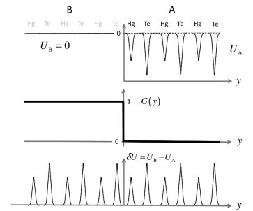
Fig. 4(a) illustrates how materials A and B are defined in the present treatment. Material A represents the TI semiconductor, which is depicted schematically along the y-direction in Fig. 4 for mercury telluride in the central plane of a HgTe/CdTe QW grown in the z-direction. If is the microscopic crystal potential in the QW, represents the potential in the wall which is treated as the vacuum or “empty crystal” with the same lattice parameter as material A. Thus , which is depicted schematically in the lower panel of Fig. 4(a). Local antibonding s- and bonding p-like band edge states in the semiconductor should thus evolve into empty crystal states of the same symmetry in the vacuum.
V.2 Four band empty crystal
In the empty crystal, antibonding s- and bonding p-like states with a given spin can be constructed directly from degenerate free electron states with wave vectors, , and , normalized to an effective unit cell volume, , as follows:(Yu and Cardona, 1996; Cardona and Pollak, 1966)
| (14a) | |||
| (14b) |
The hybridization parameter in the wall is thus:
| (15) |
which yields:
| (16a) | |||
| (16b) |
Taking = 3Å gives a value of m/s. Thus, the hybridization parameter for the wall calculated from Eq. (16b) is 6.5 eV Å, which is much smaller than the free electron Dirac value of 1973.5 eV Å.
V.3 The need for passivation
Unfortunately, a vacuum wall based on the empty crystal wave functions defined in Eq. (V.2) does not obey a Dirac-like Hamiltonian, because these wave functions are degenerate with an energy that is much higher than the energies of the band gap states in the semiconductor. Instead the wall behaves for spin up as:
| (17) |
with and . Although topological edge states are predicted from the change in Chern number or index when the semiconductor band gap inverts,(Bernevig et al., 2006; Shen et al., 2011; Enaldiev et al., 2015) this wall Hamiltonian does not ensure that the Dirac point lies in the band gap of the semiconductor. For example, the SBC wave function has no exponential solution in the wall with a real energy at .
Treatments that realize a massless Dirac like edge dispersion, including those based on OBCs(Michetti et al., 2012b) and the SBC treatment presented in this work, generally require a wall with a large band gap that overlaps that of the semiconductor. Since this does not occur with a vacuum, a passivation material is required, which should also have band edge states with opposite parity, ideally with s- and p-like symmetry, so that it behaves for spin up like with a large value of , and with (additional quadratic terms, , can also be included). A good candidate appears to be silicon dioxide (SiO2), which is the material deposited on the delineated bar-shaped sample in at least two cases where the observation of one dimensional edge states has been reported(König et al., 2008; Knez et al., 2014a). Harrison(Harrison, 1980) discusses the band structure of this material which has a band gap of approximately 9 eV. The upper valence band is composed of states which have bonding p-like symmetry, and in the cubic -cristobalite phase, they mimic the basis of the TI Hamiltonian. The conduction band is composed of an antibonding state with s-like symmetry on both the silicon and oxygen sites. The lattice parameter of the cubic unit cell is about 7.1Å, but a tetragonal version exists with a and c-parameters of 5.0 and 6.9 Å(Coh and Vanderbilt, 2008). The cubic lattice parameters for HgTe/CdTe or InAs/GaSb/AlSb QWs, are 6.5 Å and 6.1 Å, respectively, which are fairly similar to these values. It is reasonable to suppose that in the ideal case the first few atomic layers of the passivation layer will grow in registration with the TI semiconductor lattice before the SiO2 structure adopts a more complex lower energy phase. A SiO2 band gap of eV corresponds to . In addition, the difference between the electron affinities of SiO2 and HgTe or InAs is about ,(Tashmukhamedova and Yusupjanova, 2016; Voitsekhovskii et al., 2010; Hellwege and Madelung, 1982) so . Since the band edge states have the same s- and p-like symmetries as the empty crystal states in Eq. (V.2), the value of calculated above should give a correct order of magnitude. The wave function decay parameter in the SiO2 is thus approximately . This corresponds to a decay length of the order of one effective lattice parameter, , which is reasonably consistent with a wave function containing only Fourier components in the first Brillouin zone. It also shows that only a few SiO2 monolayers are required before the wave function has fully decayed, consistent with the structural assumptions made above.
If a passivation layer such as silicon dioxide is not used intentionally, it is still quite possible that a thin native oxide with a large band gap can form at an untreated wall after sample deliniation, e.g. mercury oxide and/or tellurium oxide for an HgTe/CdTe QW sample. Even here, the conduction and valence bands may be composed of the s-and p-like orbitals of the oxygen and semiconductor atoms, so it may still be possible to define a wall Hamiltonian with . An additional complication is the possible formation of trivial edge states, whose presence may well depend on the choice of surface treatment and passivation material. For example, bar samples have been fabricated from InAs/GaSb/AlSb QWs by different groups, using silicon oxide or silicon nitride (Knez et al., 2014b, a), and aluminium oxide or hafnium oxide (Nichele et al., 2016). In the second case there is evidence of edge conduction in the normal phase, suggesting that trivial edge states are present and calling into question whether this is generally the case, or dependent on which passivation material is used.
V.4 Interface band mixing
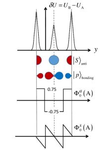
The final term of Eq. (13) contains interface potentials, , which arise because the orbitals on the boundary layer of atoms experience a different microscopic potential to their immediate neighbors. The interface potentials are evaluated as: , where the crystal periodic interface function, , is the sum of two components, the first of which has even parity and the other, odd parity, with respect to the boundary atomic plane.(Klipstein, 2010) In the example in Fig. 4 with an interface to the vacuum at , this is the plane of mercury atoms closest to the origin. The functions, , are depicted over one unit cell in the lower part of Fig. 4(b), for a mathematically abrupt interface. For a more realistic interface with a finite width they become significantly dampened, as shown in Fig. 3 of Ref. Klipstein, 2010 for an interface with a width of 0.8Å. Also shown in Fig. 4(b) are the crystal periodic perturbing potential, , as in Fig. 4(a), and the antibonding s- and bonding p-like crystal periodic functions of the reference crystal, which are depicted blue when positive and red when negative. The example in Fig. 4 is for a vacuum interface, but the perturbing potential, , can easily be modified to represent an interface with a passivation material, such as silicon dioxide whose microscopic potential is then represented by . This material is assumed to be periodic for the first one or two monolayers as discussed above, and so can be treated here with perfect periodicity because we are only interested in the interface region over the width of the delta function, , which is about one monolayer. Inspection of the symmetries in Fig. 4(b) shows that there will be four finite contributions to , namely , and , which have a finite matrix element with , and , which has a finite matrix element with . The spin up edge state wave function is the product of a hybridized crystal periodic wave function:(Klipstein, 2015) and an envelope function, , so the energy shift of the Dirac point due to the interface band mixing is approximately:
| (18) |
in which is the decay parameter of the physical edge state in the semiconductor. The dependence on the squared amplitude of the envelope function at is due to the delta function in Eq. (13), where has been replaced by . Since the wave function in the wall decays at the about the same rate as , this will lead to an overestimate, so a correction factor, , has been introduced into Eq. (18) where . The value of depends on the magnitudes and signs of the four contributions in the square bracket, which can only be estimated using microscopic calculations. Estimates for the interface band mixing potentials at a superlattice interface vary widely, and are typically in the range .Foreman (1998); Livneh et al. (2012); *LivErratum2014 Noting that where may be estimated using Eq. (12), and assuming a relatively large value of , the Dirac point is predicted to shift by = 0.004 eV when and (as in Table 3). An important point to note is that the shift of the edge state dispersion is largest at the Dirac point and decreases with increasing edge state wave vector, because it is proportional to , which vanishes at the merging points with the bulk band structure. Thus interface band mixing may shift the Dirac point and distort the edge state dispersion, but the merging points will remain fixed.
V.5 Effect of the term
Finally, the significance of the quadratic term proportional to in the first line of the multiband spin up Hamiltonian of Eq. (3) must be considered. In the present work this term has been ignored because it is quite small. For example, its inclusion causes a virtually imperceptible shift of the middle states in Fig. 2(a), of only at mid gap reducing to zero at the band edges. Moreover its matrix element with the edge state wave functions diverges due to a discontinuity in the first derivative of the wave function at the boundary, and to a contribution in the wall which tends to infinity with increasing wall potential, . Assuming that the energy of the Dirac point varies smoothly with increasing , this shows that a non-zero value of must lead to a non-exponential wave function, with a continuous first derivative and with a more linear mode of decay in the wall. This is consistent with the two band spin up model, where inclusion of the quadratic term in Eq. (3) results in the addition of to the expression for D in Eq. (4b). As for the multiband case, this has negligible effect on the dispersion of the middle states in the semiconductor. In the wall, an exponential solution requires that the band asymmetry parameter varies as , vanishing when .(Klipstein, 2015) If instead and does not vanish, the solution will again be non-exponential. There will thus be a shift in the edge state energy in both models, compared with the exponential solutions calculated for . Based on the small value of , and in the absence of an exact numerical solution, this shift is assumed to be small.
VI CONCLUSION
The four band BHZ Hamiltonian provides a simple but realistic description of the band edge states in 2D TIs such as HgTe/CdTe and InAs/GaSb/AlSb. However, the validation of hard wall boundary conditions appropriate to these materials has remained elusive. The most popular choice is OBCs which avoid any explicit treatment for the wall, while other boundary conditions tend to be phenomenological in nature, so the connection with the microscopic structure of the wall remains unclear. In this work, OBCs have been ruled out, because they fail when remote states are included explicitly in the semiconductor Hamiltonian. At the same time, the other boundary conditions show that a wide variety of edge state dispersions are possible, depending on the values of the phenomenological parameters. Therefore a different approach has been adopted here, based on SBCs which address more directly both the microscopic properties of the wall, and the conditions that can lead to a Dirac point in the semiconductor band gap.
The use of OBCs leads to contactless edge confinement, and a Dirac point with an unphysical dependence on the TI band parameters. Other unphysical results have also been reported when these boundary conditions are used,(Klipstein, 2018) and further aspects are discussed in Appendix B. Although mathematically correct, it is known that one of the two gap solutions for a given spin direction is spurious. Unfortunately, this solution must be combined with the physical gap solution in order to satisfy OBCs, and such combination is only possible because both solutions have the same eigenvector. The spurious solution is related to diagonal k-quadratic terms which are introduced into the BHZ Hamiltonian when remote states are eliminated using perturbation theory. If the remote states are not eliminated but included in a larger, multiband Hamiltonian, the eigenvectors of the two gap solutions are no longer equal and an OBC solution is impossible. This is because the spurious solution is replaced by a physical solution with large eigenvector components from the remote states.
An alternative approach suggested previously by the author is to use SBCs. These boundary conditions match both the wave function and the product of its derivative and a reciprocal mass term at the interface between the semiconductor and the wall, and are obtained by integrating the BHZ Hamiltonian across the boundary region. Unlike other SBC treatments which have been applied to a soft wall and which evolve into OBCs when the wall becomes hard, the present SBC approach is for a hard wall and results in wave function confinement with a large amplitude at the edge. This type of confinement is typical of other classic surface phenomena, such as surface plasmons and phonons. The SBC edge state wave function is constructed from just the physical gap solutions on each side of the boundary. It has been verified in the present work by comparison with a multiband solution, with which it is in complete agreement. In both cases, the Dirac point has a dependence on the TI band parameters that is physically justifiable.
One of the challenges of the SBC approach is to establish the strength of the electron-hole hybridization in the wall. When the semiconductor and wall have the same mid gap energies but different hybridization parameters, the Dirac point is slightly shifted from mid gap. In this work the wall was considered initially as an empty crystal, with a free electron basis that matches the symmetry of the antibonding s-states and bonding p-states in the semiconductor. This establishes an estimate for the wall hybridization parameter that behaves like the free electron Dirac value, , but with the speed of light, c, replaced by the velocity, in which is the monolayer thickness in the semiconductor. The wall hybridization parameter is then about 6.5 eV Å, which is comparable to the semiconductor value. The empty crystal Hamiltonian represents a hard vacuum like wall, but unfortunately there is no splitting between the electron and hole states, which are also much higher in energy than those in the semiconductor. In order to ensure edge states with a Dirac point that lies in the semiconductor band gap, it appears that a thin passivation layer is required, which may be the native oxide of the material, or an externally deposited dielectric material such as silicon dioxide, for which successful observations of the quantum spin Hall effect have been reported. Silicon dioxide indeed has bands of the correct s- and p-like symmetry separated by a large band gap that overlaps that of the semiconductor fairly symmetrically. Assuming a pseudomorphic cubic phase immediately next to the semiconductor, its hybridization parameter should have a similar magnitude to that estimated for the s- and p-states of the empty crystal. The nature of the passivation layer may also be important to avoid the presence of trivial edge states.
Another challenge in the SBC approach is that the mode of decay of the edge state wave function is generally non-exponential. Nevertheless, it is possible to find useful exponential solutions when the wall is effectively infinite, , and the edge state decay parameter is real as in HgTe/CdTe QWs. Although this has been the main focus of the present work, it was also confirmed that weakly hybridized systems with a complex decay parameter, such as InAs/GaSb/AlSb, exhibit non-exponential behavior when the band structure is asymmetric. Even for weakly hybridized systems with a symmetric band structure, SBCs have been shown previously to exhibit non-exponential behavior in narrow samples, except at certain characteristic widths.(Klipstein, 2018)
The shift of the Dirac point from mid gap is generally small when SBCs are used with wall passivation. However, several additional factors could affect its position, including the small quadratic term left out of the multiband Hamiltonian (see Sec. V), the difference in the mid gap energies of the semiconductor and passivation materials ( in Eq. (17)), and the effect of interface band mixing. The first two factors should not be too significant, especially if a passivation material is used with , but the third could be important, producing a shift which is greatest at the Dirac point and which steadily decreases to zero at the wave vectors where the edge state dispersion merges with the bulk band edges. Microscopic calculations of the interface band mixing potentials are therefore needed to establish the size of this effect.
In summary, the present work has demonstrated that OBCs must be replaced by boundary conditions that allow stronger edge confinement with a large amplitude of the wave function at the sample edge, and that this results in a modified edge state dispersion. In addition, a passivation layer is often present, either intentionally or due to the formation of a native oxide, and it was found that this may even be an essential way of ensuring that the Dirac point lies in the semiconductor band gap. Although scattering from edge imperfections is suppressed by time reversal symmetry, a practical consequence of the present hard wall SBC approach is that stronger wave function confinement, combined with significant disorder in the passivation layer, could both lead to a lower threshold for the breakdown of dissipationless transport than previously thought.(Pezo et al., 2020)
Acknowledgements.
The author acknowledges useful correspondence with Dr. M. V. Durnev.Appendix A Full edge state dispersion in the multiband model
The full spin up edge state dispersion, is calculated by finding solutions for with the same eigenvectors on both sides of the boundary. Assuming and writing , Eq. (3) can be solved for the decay parameter, , and eigenvector, [a, b, c, d] in the semiconductor in terms of the energy, E, and wave vector, to yield the relations in Table 4, where:
| Decay Parameter | Eigenvector |
|---|---|
| (19a) | |||
| (19b) | |||
| (19c) | |||
| (19d) | |||
| (19e) | |||
| (19f) | |||
| (19g) |
and in the semiconductor. In the wall and the corresponding parameters are , , , , , , and . The relations in Table 4 can be expressed in terms of these parameters and rearranged to yield the band gap ratios in the wall that correspond to a specific eigenvector:
| (20a) | |||
| (20b) |
It is clear that these ratios become independent of the wall band gap, , when , since E has the same order of magnitude as the semiconductor band gap parameter, M, so as . For given values of E and , the semiconductor eigenvector components are calculated according to the relations in Table 4 and inserted into Eq. (A). This yields the wall band gaps for a given set of wall hybridization parameters, and . These band gaps should be substituted back into the relations in Table 4 and the process repeated at different energies until the wall eigenvector comes out to be the same as the semiconductor eigenvector, giving a self-consistent solution at the chosen wave vector. The values of the decay parameters in the semiconductor and wall can also be found for each point on the dispersion curve, using the formula in the left hand column of Table 4.
As discussed in Sec. II, it appears to be a typical feature of SBC edge states that an exponential solution only exists when specific wall parameters have a certain ratio with the wall band gap. In the two band case, the parameters in question are and , where a useful exponential solution can be found in the infinite wall limit when . For other ratios of the wall parameters, a numerical approach must be used. The multiband spin up model exhibits similar features, where an exponential solution exists for the wall band gaps given by Eq. (A), giving a useful exponential solution in the limit: as . Practically, this “hard wall” limit corresponds to , which is already obeyed very well for in the examples discussed below.444This is also true for solutions derived with and interchanged in the Q-terms of Eq. (3), corresponding to a change in symmetry of the remote states. Note that the interchange leads to similar but modified expressions for the eigenvectors in Table 4 and the band gap ratios in Eq. (A).
The blue dashed curves in Fig. 5 show three examples of the spin up edge state dispersions calculated for symmetric or asymmetric semiconductor band structures. In each case, the wall parameters are = 20 eV, = 11 eV Å, and 2 eV Å, where and have the same order of magnitude as the values estimated for a passivation material in Sec. V. In all three cases the dispersions are insensitive to a variation in the value of the wall band gap by a factor of greater than 0.05 (corresponding to ). In Fig. 5(a), the semiconductor parameters are the same as in Table 2 for a symmetric TI band structure. The open circles depict a variation of the form: , and there is virtually no difference between this variation and the blue dashed curve, showing that the dispersion calculated from the four band spin up model has the same linear variation as for the two band case. The red dashed curve is for the spin down edge state and is obtained from the blue curve by time reversal.
 |
 |
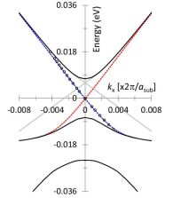 |
| (a) | (b) | (c) |
 |
 |
| (a) | (b) |
In Fig. 5(b), the outer band gap in the semiconductor is reduced to . Based on Eq. (4b), this is equivalent to for the two band case. All other parameters in the wall and semiconductor are the same as for Fig. 5(a), and except near the band edges, the multiband result is still very close to the circles which depict the two band variation, . Fig. 5(c) shows an example with asymmetric semiconductor band parameters, as listed in the left hand column of Table 3. As already discussed for this case in Sec. IV, the Dirac point is very close to mid gap, with an energy of . Using this value as an estimate for the two band Dirac point energy, the open circles in Fig. 5(c) depict the dispersion based on the two band spin up result, , where the square root in Eq. (11) is very close to unity. The two band spin up dispersion again agrees quite well with the calculated multiband result.
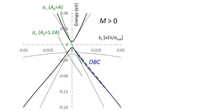
The OBC dispersion, given by Eq. (9), may be compared with the SBC results in Fig. 5. It is the same as the open circles for the symmetric cases in Figs. 5(a) and 5(b) but very different for the asymmetric case in Fig. 5(c), where it is shown as gray lines. For the asymmetric case, the Dirac point is strongly shifted toward the conduction band and the edge state dispersion is linear with a much reduced phase velocity.
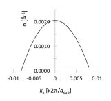
The wave vector dependence of the spin up decay parameters in the multiband treatment is shown in Fig. 6, where it is compared for the symmetric and asymmetric cases shown in Figs. 5(a) and 5(c), respectively. The wave vectors of the merging points can clearly be identified where . In both cases, the decay parameter at the Dirac point agrees with Eq. (12) which has a value close to when as in these examples. For the symmetric case, the two band model corresponds fairly well with the multiband model over the whole wave vector range, with merging points in the two band model at . For the asymmetric case, however, the two band model gives merging points at , while the magnitudes of the merging wave vectors in Fig. 6(b) are similar to these values but unequal. This can be attributed to stronger band non-parabolicities in the asymmetric multiband model.
All of the edge dispersions in Figs. 5 and 6 are based on middle wave vector solutions in the wall and semiconductor. As mentioned in Sec. III, when the wing solutions are used in the asymmetric two band spin up model, they only yield an edge state when D < B, which then has an anomalous dispersion, as shown for example with in Fig. 2(a) of Ref. Klipstein, 2015. This is also true in the four band spin up model. Using parameters corresponding to Fig. 5(c) but with , the edge dispersion fails to cross or merge with the bulk bands, and no exponential edge state can be found for . Therefore, this edge state can be considered unphysical even though, in principle, the four band spin up Hamiltonian gives physical wing solutions, as shown, for example, in Fig. 2(b). This behavior is related to the large magnitude of the imaginary wing wave vector in the wall Hamiltonian, which tends to infinity as . Even for large but finite values of these parameters, its magnitude is well beyond the boundary of the Brillouin zone, so a hard wall edge state based on the wing solutions cannot be described physically, even with four bands.
Finally, it should be noted that the band gap ratios in Eq. (A) that correspond to exponential edge state solutions are k-dependent, so the outer bands have a significant dispersion even when the inner bands do not (i.e. constant ). Since all bands in the wall are effectively at infinity, and the results in Fig. 5 are totally insensitive to the positions of the inner bands for , it is anticipated that the effect of the outer band positions on the energy dispersions should not be too significant. Nevertheless, in order to test this assumption a full numerical treatment is needed for constant values of all the wall band gaps, when the wave function will generally exhibit a non-exponential decay.
Appendix B Topologically trivial edge solutions
It has recently been pointed out that edge states can be found for the BHZ Hamiltonian in the topologically trivial phase, with .(Candido et al., 2020) In this Appendix, such behavior is confirmed for both OBC and SBC boundary conditions. However, all such states include the wing solution and are therefore unlikely to exist in any real physical system. No edge state can be found using SBCs based only on the physical middle solution.
The band structure near the bulk band gap of a topologically trivial insulator is shown in gray in Fig. 7, for an eight band Hamiltonian with , , and . The conduction and valence bands of the BHZ Hamiltonian are superimposed in black, with quadratic coefficients, and , calculated from Eq. (4b). It can be seen that for wave vectors beyond the range allowed by perturbation theory, , the conduction and valence bands of the BHZ Hamiltonian deviate strongly from those of the full eight band Hamiltonian (see Sec I). Therefore results of the BHZ Hamiltonian are only reliable in this small wave vector range.
Exponential BHZ edge states can be determined using the OBC and SBC characteristic equations, (8) and (10), respectively. For OBCs, a topologically trivial edge solution exists with real decay parameters when . The dispersion, shown as a blue dashed line in Fig. 7, reproduces very well the form of the dispersion shown in Fig. 1(a) of Ref. Candido et al., 2020.555Note that the BHZ Hamiltonian used in Ref. Candido et al., 2020 corresponds to spin down in this work A topologically trivial SBC edge solution can also be found, for the wing decay parameter, , in Eq. (10). Its dispersion is plotted near the zone center, as green dashed and dotted lines, respectively, for wall hybridization parameters of and . The solution for is in fact very similar to the spurious solution shown for the TI phase in Fig. 2(a) of Ref. Klipstein, 2015. This is because in Eq. (10), so the sign of M becomes unimportant. Noting that Eq. (10) corresponds to a wall with negative , a finite wall with positive can be intercalated next to the TI, so that the edge state localizes on the interface between wall materials for which , separating from the sample edge for which (analogous to Fig. 3 and Ref. Klipstein, 2018). This confirms that the edge state is not a physical solution. In addition to a wave function that includes the unphysical wing solution, both the OBC and SBC edge states extend to wave vectors far beyond the limit. In contrast, when SBCs are used in Eq. (10) with the physical, decay parameter, there is no topologically trivial solution. This is consistent with , allowing only a single edge state, which is the unphysical, solution.666This is also consistent with the mutiband model. For positive , with , semiconductor parameters as in Fig. 7, and , the only eigenvectors at zero energy and wave vector that are nearly similar on each side of the boundary are those for the wing solution, and only for , when the outer band gap parameters change sign (consistent with negative and in the four band model). Since is negative there is no exponential solution (see Sec. IIC). However, given that the eigenvectors are very close, namely in the wall and in the semiconductor, this suggests that a nearby non-exponential edge state exists in the multiband model, corresponding to the wing solution of the topologically trivial phase.
In Ref. Candido et al., 2020, edge states appear in the topologically trivial phase for any value, apart from , of a independent, phenomenological boundary condition parameter, , which is conserved across the phase boundary, and whose value depends on the boundary conditions used for the envelope function. For OBC edge states as in Fig. 7, is a function of and is indeed independent of wave vector and the sign of the band gap parameter, M. For SBCs in the TI phase, with negative M, , and other parameters as in Fig. 7, the physical edge state behaves as , with at , and at the merging points. The value of is quite insensitive to an increase in the wall hybridization parameter and always tends to one at the merging points. When there is charge conjugation symmetry with and a linear edge dispersion, for all . Thus, even in the presence of strong band asymmetry, the behavior of the physical SBC solution is very close to the special case of , where no edge state exists in the topologically trivial phase. The paradoxical appearance of edge states in the topologically trivial phase may therefore be a mathematical artifact associated with the spurious wing solution.
References
- Yu and Cardona (1996) P. Yu and M. Cardona, Fundamentals of Semiconductors, Physics and Material Properties (Springer Verlag, Berlin, 1996).
- Ritchie (1957) R. H. Ritchie, Phys. Rev. 106, 874 (1957).
- Pitarke et al. (2007) J. M. Pitarke, V. M. Silkin, E. V. Chulkov, and P. M. Echenique, Rep. Prog. Phys. 70, 1 (2007).
- Fuchs and Kliewer (1965) R. Fuchs and K. L. Kliewer, Phys. Rev. 140, A2076 (1965).
- Sood et al. (1985) A. K. Sood, J. Menendez, M. Cardona, and K. Ploog, Phys. Rev. Lett. 54, 2115 (1985).
- Qi and Zhang (2010) X.-L. Qi and S.-C. Zhang, Physics Today 63, 33 (2010).
- Bernevig et al. (2006) B. A. Bernevig, T. L. Hughes, and S.-C. Zhang, Science 314, 1757 (2006).
- König et al. (2008) M. König, H. Buhmann, L. W. Molenkamp, T. L. Hughes, C.-X. Liu, X.-L. Qi, and S.-C. Zhang, J. Phys. Soc. Jpn. 77, 031007 (2008).
- Nichele et al. (2016) F. Nichele, H. J. Suominen, M. Kjaergaard, C. M. Marcus, E. Sajadi, J. A. Folk, F. Qu, A. J. A. Beukman, F. K. de Vries, J. van Veen, S. Nadj-Perge, L. P. Kouwenhouven, B.-M. Nguyen, A. A. Kisilev, W. Yi, M. Sokolovich, M. J. Manfra, E. M. Spanton, and K. A. Moler, New. Journ. Phys. 18, 083005 (2016).
- Klipstein (2015) P. C. Klipstein, Phys. Rev. B 91, 035310 (2015).
- (11) (erratum), Phys. Rev. B 93, 199905 (2016).
- Tkachov and Hankiewicz (2010) G. Tkachov and E. M. Hankiewicz, Phs. Rev. Lett. 104, 166803 (2010).
- Tkachov and Hankiewicz (2013) G. Tkachov and E. M. Hankiewicz, Phys. Staus. Solidi B 250, 215 (2013).
- Medhi and Shenoy (2012) A. Medhi and V. B. Shenoy, J. Phys.: Condens. Matter 24, 355001 (2012).
- Zhou et al. (2008) B. Zhou, H.-Z. Li, R.-L. Chu, S.-Q. Shen, and Q. Niu, Phys. Rev. Lett. 101, 246807 (2008).
- Essert (2015) S. Essert, Ph.D. thesis, Univ. of Regensberg (2015).
- Qi et al. (2006) X.-L. Qi, Y.-S. Wu, and S.-C. Zhang, Phys. Rev. B 74, 085308 (2006).
- König et al. (2007) M. König, S. Wiedmann, C. Brüne, A. Roth, H. Buhmann, L. W. Molenkamp, X.-L. Qi, and S.-C. Zhang, Science 318, 766 (2007).
- Dai et al. (2008) X. Dai, T. L. Hughes, X.-L. Qi, Z. Fang, and S.-C. Zhang, Phys. Rev. B 77, 125319 (2008).
- Liu et al. (2008) C.-X. Liu, T. L. Hughes, X.-L. Qi, K. Wang, and S.-C. Zhang, Phys. Rev. Lett. 100, 236601 (2008).
- Linder et al. (2009) J. Linder, T. Yokoyama, and A. Sudbø, Phys. Rev. B 80, 205401 (2009).
- Liu et al. (2010) C.-X. Liu, X.-L. Qi, H.-J. Zhang, X. Dai, Z. Fang, and S.-C. Zhang, Phys. Rev. B 82, 045122 (2010).
- Lu et al. (2010) H. Z. Lu, W. Y. Shan, W. Yao, Q. Niu, and S. Q. Shen, Phys. Rev. B 81, 115407 (2010).
- Shan et al. (2010) W. Y. Shan, H. Z. Lu, and S. Q. Shen, New. Journal of Physics 12, 043048 (2010).
- Sonin (2010) E. B. Sonin, Phys. Rev. B. 82, 113307 (2010).
- Murakami (2011) S. Murakami, J. Phys.: Conference Series 302, 012019 (2011).
- Shen et al. (2011) S. Q. Shen, W. Y. Shan, and H. Lu, Spin 1, 33 (2011).
- Wada et al. (2011) M. Wada, S. Murakami, F. Freimuth, and G. Bihlmayer, Phys. Rev. B 83, 121301 (2011).
- Michetti et al. (2012a) P. Michetti, J. C. Budich, E. G. Novik, and P. Recher, Phys. Rev. B 85, 125309 (2012a).
- Michetti et al. (2012b) P. Michetti, P. H. Penteado, J. C. Egues, and P. Recher, Semicond. Sci. Technol. 27, 124007 (2012b).
- Takagaki (2012) Y. Takagaki, J. Phys.: Condens Matter 24, 435301 (2012).
- Cano-Corte’s et al. (2013) L. Cano-Corte’s, C. Ortix, and J. van den Brink, Phys. Rev. Lett. 111, 146801 (2013).
- Hohenadler and Assaad (2013) M. Hohenadler and F. F. Assaad, J. Phys.: Condens. Matter 25, 143201 (2013).
- Sengupta et al. (2013) P. Sengupta, K. Tillmann, T. Yaohua, M. Povolotskyi, and G. Klimeck, Journ. of Appl. Phys. 114, 043702 (2013).
- Wang et al. (2014) J. Wang, Y. Xu, and S.-C. Zhang, Physical Review B 90, 054503 (2014).
- Xu et al. (2014) D.-H. Xu, J.-H. Gao, C.-X. Liu, J.-H. Sun, F.-C. Zhang, and Y. Zhou, Phys. Rev. B 89, 195104 (2014).
- Enaldiev et al. (2015) V. V. Enaldiev, I. V. Zagorodnev, and V. A. Volkov, JETP Letters 101, 89 (2015).
- Durnev and Tarasenko (2016) M. V. Durnev and S. A. Tarasenko, Phys. Rev. B 93, 075434 (2016).
- Entin et al. (2017) M. V. Entin, L. I. Magarill, and M. Mahmoodian, Europhysics Letters 118, 57002 (2017).
- Candido et al. (2020) D. R. Candido, M. Kharitonov, J. C. Egues, and E. M. Hankiewicz, Phys. Rev. B. 98, 161111 (2020).
- Gioia et al. (2018) L. Gioia, U. Zülicke, M. Governale, and R. Winkler, Phys. Rev. B 97, 205421 (2018).
- Durnev and Tarasenko (2019) M. V. Durnev and S. A. Tarasenko, Ann. Phys. 531, 1800418 (2019).
- Gioia et al. (2019) L. Gioia, M. G. Christie, U. Zülicke, M. Governale, and A. J. Sneyd, Phys. Rev. B 100, 205417 (2019).
- Böttcher et al. (2020) J. Böttcher, C. Tutschku, and E. M. Hankiewicz, Phys. Rev. B 101, 195433 (2020).
- Durnev (2020) M. V. Durnev, Phys. Solid State 62, 504 (2020).
- Kane (2013) C. H. Kane, in Contemporary Concepts of Condensed Matter Science, Vol. 6, edited by M. Franz and L. Molenkamp (Elsevier, Amsterdam, 2013) Chap. 1.
- Klipstein (2010) P. C. Klipstein, Phys. Rev. B 81, 235314 (2010).
- White and Sham (1981) S. R. White and L. J. Sham, Phys. Rev. Lett. 47, 879 (1981).
- Schuurmans and t’Hooft (1985) M. F. H. Schuurmans and G. W. t’Hooft, Phys. Rev. B 31, 8041 (1985).
- Note (1) A physical dispersion must be evanescent in the band gap, starting and finishing at a band edge.
- Klipstein (2018) P. C. Klipstein, J.Phys.: Condens. Matter 30, 275302 (2018).
- Luttinger and Kohn (1955) J. M. Luttinger and W. Kohn, Phys. Rev. 97, 869 (1955).
- Volkov and Takhtamirov (1997) V. A. Volkov and É. E. Takhtamirov, Physics-Uspekhi 40, 1071 (1997).
- Takhtamirov and Volkov (1997) É. E. Takhtamirov and V. A. Volkov, Semicond. Sci. and Technol. 12, 77 (1997).
- Takhtamirov and Volkov (1999) É. E. Takhtamirov and V. A. Volkov, JETP 89, 1000 (1999).
- Cardona and Pollak (1966) M. Cardona and F. H. Pollak, Phys. Rev. 142, 530 (1966).
- Bir and Pikus (1974) G. L. Bir and G. E. Pikus, Symmetry and Strain induced effects in semiconductors (Wiley, New York, 1974).
- Note (2) If and are interchanged in the Q-terms of Eq. (3\@@italiccorr), corresponding to a change in symmetry of the remote states, there is no change to the energy of the Dirac point based on the present multiband model, and the edge state dispersions are essentially the same as those derived in Appendix A.
- Lawaetz (1971) P. Lawaetz, Phys. Rev. B. 4, 3460 (1971).
- Klipstein (2016) P. C. Klipstein, J. Phys.: Condens. Matter 28, 375801 (2016).
- Note (3) Even though the wing solution of the four band spin up Hamiltonian is not necessarily spurious, the reason it gives an unphysical edge state is discussed at the end of Appendix A.
- Knez et al. (2014a) I. Knez, C. I. Rettner, S.-H. Yang, S. S. P. Parkin, L. Du, R.-R. Du, and G. Sullivan, Phys. Rev. Lett. 112, 026602 (2014a).
- Harrison (1980) W. A. Harrison, “Electronic structure and the properties of solids: the physics of the chemical bond,” (W. H. Freeman and Co., San Francisco, 1980) Chap. 11-D, pp. 267–270.
- Coh and Vanderbilt (2008) S. Coh and D. Vanderbilt, Phys Rev. B 78, 054117 (2008).
- Tashmukhamedova and Yusupjanova (2016) D. A. Tashmukhamedova and M. B. Yusupjanova, Journ. Surface Investigation. X-ray, Synchrotron and Neutron Techniques 10, 1273 (2016).
- Voitsekhovskii et al. (2010) A. V. Voitsekhovskii, D. I. Gorn, S. N. Nesmelov, and A. P. Kokhanenko, Opto-electronics Review 18, 241 (2010).
- Hellwege and Madelung (1982) K. H. Hellwege and O. Madelung, eds., Physics of Group IV elements and III-V Compounds, Landolt-Börnstein New Series, Group III, Vol. 17a (Springer Verlag, Berlin, 1982).
- Knez et al. (2014b) I. Knez, R.-R. Du, and G. Sullivan, Phys. Rev. B 81, 201301 (2014b).
- Foreman (1998) B. A. Foreman, Phys. Rev. Lett. 81, 425 (1998).
- Livneh et al. (2012) Y. Livneh, P. C. Klipstein, O. Klin, N. Snapi, S. Grossman, A. Glozman, and E. Weiss, Phys. Rev. B 86, 235311 (2012).
- (71) (erratum), Phys. Rev. B 90, 039903 (2014).
- Pezo et al. (2020) A. Pezo, B. Focassio, G. R. Schleder, M. Costa, C. Lewenkopf, and A. Fazzio, arXiv:2010.11693 (2020).
- Note (4) This is also true for solutions derived with and interchanged in the Q-terms of Eq. (3\@@italiccorr), corresponding to a change in symmetry of the remote states. Note that the interchange leads to similar but modified expressions for the eigenvectors in Table 4 and the band gap ratios in Eq. (A\@@italiccorr).
- Note (5) Note that the BHZ Hamiltonian used in Ref. \rev@citealpnumCandido2018 corresponds to spin down in this work.
- Note (6) This is also consistent with the mutiband model. For positive , with , semiconductor parameters as in Fig. 7, and , the only eigenvectors at zero energy and wave vector that are nearly similar on each side of the boundary are those for the wing solution, and only for , when the outer band gap parameters change sign (consistent with negative and in the four band model). Since is negative there is no exponential solution (see Sec. IIC). However, given that the eigenvectors are very close, namely in the wall and in the semiconductor, this suggests that a nearby non-exponential edge state exists in the multiband model, corresponding to the wing solution of the topologically trivial phase.