book\newunit
An in-plane photoelectric effect in two-dimensional electron systems for terahertz detection
Abstract
The photoelectric effect consists in the photoexcitation of electrons above a potential barrier at a material interface and is exploited for photodetection over a wide frequency range. This three-dimensional process has an inherent inefficiency: photoexcited electrons gain momenta predominantly parallel to the interface, while to leave the material they have to move perpendicular to it. Here, we report on the discovery of an in-plane photoelectric effect occurring within a two-dimensional electron gas. In this purely quantum-mechanical, scattering-free process, photoelectron momenta are perfectly aligned with the desired direction of motion. The “work function” is artificially created and tunable in-situ. The phenomenon is utilized to build a direct terahertz detector, which yields a giant zero-bias photoresponse that exceeds the predictions by known mechanisms by more than 10-fold. This new aspect of light-matter interaction in two-dimensional systems paves the way towards a new class of highly efficient photodetectors covering the entire terahertz range.
1 Introduction
A key milestone in the history of quantum mechanics was the discovery of the photoelectric effect [1]: a photon excites an electron from the surface of a metal, if its quantized energy is larger than the metal’s workfunction [2]. Apart from this external photoelectric effect, at lower frequencies (far infrared – visible) photoexcitation of electrons into higher-energy quantum states within a semiconductor can lead to a photoresponse of the material, which is an internal photoeffect.
The photoemission from a material in three dimensions is a complicated process consisting of several steps [3, 4]: first photons excite electrons, these then move and scatter within the solid, and finally leave into the collecting medium provided they have sufficient energy and momentum perpendicular to the interface. This leads to its inherent inefficiency: the photoexcited electrons gain predominantly a momentum parallel to the electric field [5] and thus parallel to the surface under normal incidence of radiation. Electrons can obtain a perpendicular momentum component, needed to escape from the material, under oblique incidence of p-polarised light [4, 6, 7], or by scattering processes that randomise the direction of motion of photoexcited electrons [3]. But scattering reduces their energy, diminishes the efficiency, and limits the intrinsic response time of the effect to scattering times.
Being a fundamental physical phenomenon converting light (photons) to electricity, the photoelectric effect can be exploited for detection of electromagnetic radiation over a wide range of frequencies. In the mid- and far infrared ranges, it has been used in internal photoemissive detectors [8, 9, 10, 11]. However, the responsivity of homojunction and heterojunction internal photoemission detectors rapidly falls off below 5 THz, essentially vanishing below 2.5 THz [12, 13, 14]. Furthermore, these three-dimensional, bulk photoemissive detectors are photoconductive and thus require an applied external bias [15, 16, 17, 14].
In this paper, we report on a giant, direct THz photoresponse in a two-dimensional electron gas (2DEG). In our devices, we cover a 2DEG in a semiconductor heterostructure with two gates which simultaneously serve as a terahertz (THz) antenna. By applying different voltages to the gates, we create a potential step for electrons within the plane of the 2D channel. Under THz irradiation, which is normally incident on the semiconductor surface, electrons are then instantaneously excited above the potential step, which leads to a giant photocurrent and photovoltage response under zero source-drain bias. The electric field of the wave and the desired direction of photoelectron momentum are perfectly aligned in the same direction, parallel to the surface. We will call this the in-plane photoelectric effect (not to be confused with the lateral photoelectric effect [18], an unrelated phenomenon). It is a direct quantum-mechanical, scattering-free process, which thus does not have an intrinsic response time limit due to scattering. The height of the potential step, an analog of the work function in our device, is electrically tunable in situ by applying different voltages to the gates.
Previously, THz detection in 2DEGs and structures based on those has been realised using various mechanisms, in III-V and silicon semiconductors [19, 20, 21, 22, 23, 24, 25, 26, 27, 28, 29, 30, 31, 32, 33], as well as, more recently, also in novel 2D materials [34, 35, 36]. The discovered effect we report is more than 10-fold as strong as predicted by the classical plasmonic mixing [37, 26] in two-dimensional systems, and cannot be explained by other mechanisms such as photon-assisted tunneling [38, 33], bolometric, electron heating [27, 31], or thermoelectric effects [19]. We develop a quantum theory of the in-plane photoelectric effect which describes the experimental findings very well. We show that the discovered phenomenon is ideally suited for highly efficient photodetection across the entire terahertz range.
2 Results
2.1 Physics of the phenomenon
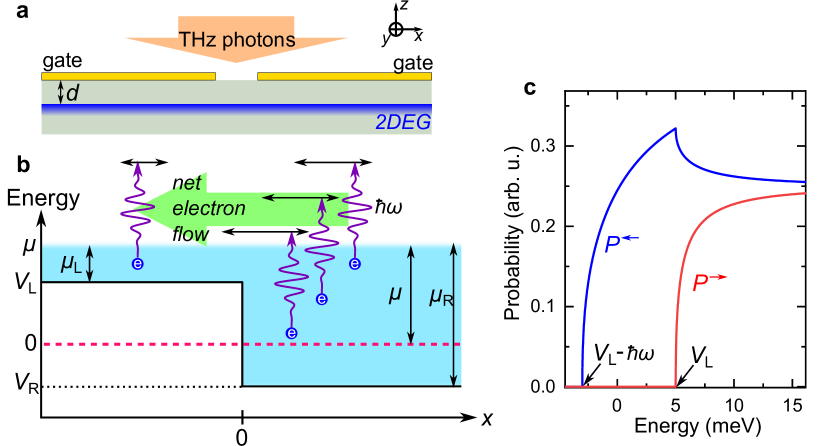
Consider a uniform 2DEG covered by two gates, see Fig. 1 (a). In equilibrium, the bottom of the conduction band (dashed purple line) and the chemical potential are position-independent. By applying two different voltages on the gates, and , we create an artificial, gate voltage tunable potential step for electrons moving in the 2DEG. This shifts the bottom of the equilibrium conduction band under the left and right gates by and , respectively, resulting in the local chemical potentials and , see Fig. 1 (b). Without any incident radiation, the net particle flow vanishes: electrons with energies do not contribute to the current since they are reflected backwards at the step, while for the current flow cancels out due to equal reflection and transmission probabilities regardless of the direction of electron motion.
Once the potential step in the gap between the gates is exposed to incident electromagnetic radiation of frequency , electrons can absorb a photon of energy . Those with energies on the right side, that previously could not overcome the step, are now able to do so by absorbing incident photons. For electrons with energies , photon absorption will lead to a higher probability to move to the left (onto the step) than to the right, see Fig. 1 (c). As a result, the radiation induces a net particle flow from the higher-density region to the lower-density region. This can be understood as a photoelectric effect occuring within the plane of the 2DEG.
This phenomenon can be used for detection of far-infrared and terahertz radiation. We utilize the in-plane photoelectric effect for THz detection in a 2DEG covered by two gates that simultaneously serve as a THz antenna.
2.2 Samples and setup
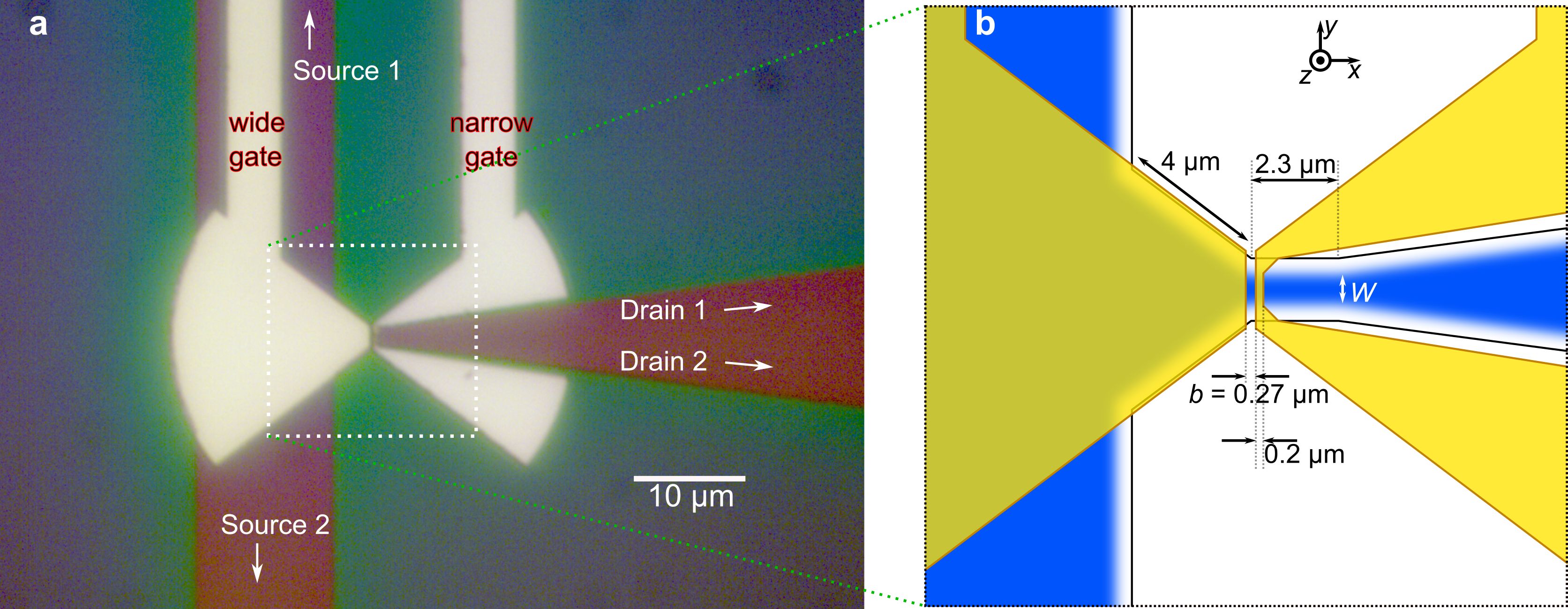
Our samples, see Fig. 2 (a), are fabricated from a GaAs-Al0.33Ga0.67As heterostructure grown by molecular beam epitaxy (see details in Methods section). The 2DEG in the wafer material, nm below the surface, exhibits an electron density of cm2 and a mobility of cm2/(Vs) at 1.5 K, corresponding to a scattering time of ps and a mean free path of 20 µm. Narrow channels were created by mesa etching. The active part of the device, see Fig. 2 (b), is covered by a bow-tie antenna that couples THz radiation to the 2DEG. The right part of the antenna, the “narrow gate”, is split into two halves that are joined together via a 200 nm narrow bridge, Fig. 2 (b). Both wings of the antenna serve as gates in our device. The 2DEG has four Ohmic contacts, labelled Source 1 or 2, and Drain 1 or 2, which are at least 100 µm away from the center of the antenna to avoid their influence on the active part of the device.
The devices were cooled to 9 K in a liquid helium continuous flow cryostat. A copper waveguide system delivered 1.9 THz radiation from a quantum cascade laser (QCL) source [39, 40] to the samples. The QCL is electrically modulated with a modulation frequency of Hz and a duty cycle of 2.14 %. The time-averaged intensity incident on the sample is (for details see Methods section) µW/mm2. Within a pulse, the intensity is mW/mm2.
2.3 Photoresponse and device parameters
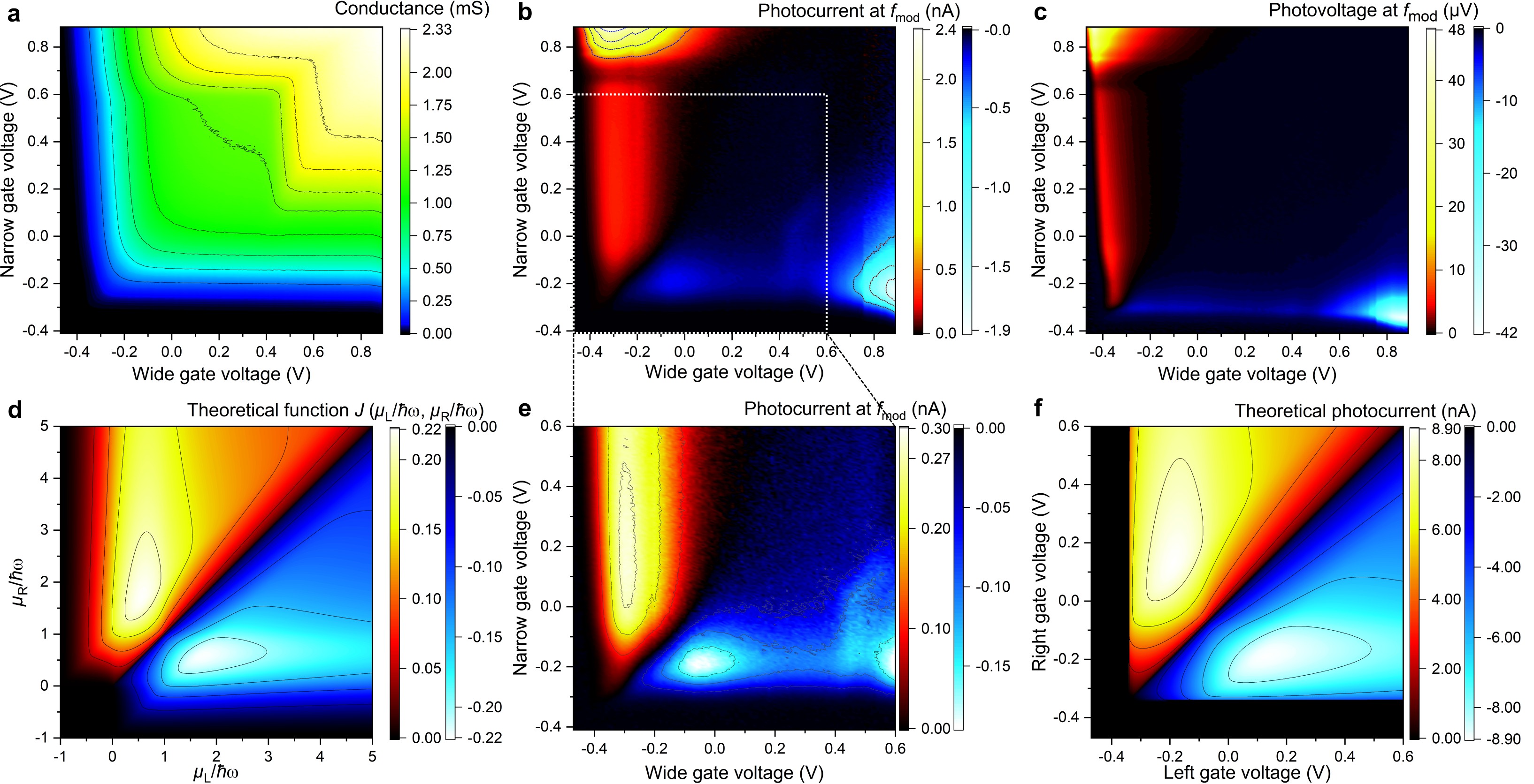
Fig. 3 (a) illustrates the conductance of the sample, measured in a 4-terminal configuration, as a function of the two gate voltages in a 2D colormap. At zero gate voltages, the 4-wire channel resistance is k\textOmega. The conductance vanishes at the left and at the bottom of the map, which corresponds to the pinch-off of the channel using the wide or narrow gate, respectively. The threshold voltage determined from the wide gate is V; here the 4-wire channel resistance is 16 times higher than . The channel is switched off for V, where the resistance exceeds 1 M\textOmega. corresponds to an equilibrium electron density of and an equilibrium chemical potential of , with and the effective electron mass in GaAs [41].
Under incident THz radiation, the sample generates a photoresponse. The induced current under zero source-drain bias in a short-circuit measurement, the photocurrent, is shown in Fig. 3 (b). The photovoltage acquired in an open-circuit measurement is depicted in Fig. 3 (c). The measurement is done using a lock-in amplifier with the QCL modulation frequency as reference. The red and blue color schemes indicate areas where the response is positive or negative, respectively.
The photoresponse arises predominantly in the left or bottom areas in the 2D maps Fig. 3 (b) and (c), where either of the narrow or wide gate voltages are negative. Here, one of the gates depletes the 2DEG, which gives rise to a potential step in the channel. The sign of the photoresponse is always such that the THz-induced electron flow moves onto the potential step, from the higher density region to the lower density region. The photoresponse is mostly anti-symmetric with respect to the diagonal line . Two regimes can be identified: (i) and V, shown in detail in Fig. 3 (e), and (ii) or V, where the photoresponse increases strongly in the top-left and bottom-right corners. The latter regime corresponds to strong asymmetry of the gates, where one of the gates operates in the depletion regime with a negative voltage applied with respect to the source Ohmic contact, while the other gate has a strong positive voltage applied and operates in the enhancement mode.
A further increase in the gate voltage, beyond V and V, leads to the onset of a rapidly growing gate leakage. In this regime, undesirable for detector operation, the sample becomes unstable and noisy. Blocking and unblocking the incident THz radiation did not result in any change (within measurement accuracy of 10 pA) of the gate currents. This excludes gate currents as a possible origin of the photoresponse, e. g. due to Schottky barrier rectification.
A negative voltage on the narrow gate creates a barrier of 0.2 µm width, whereas on the wide gate it creates a µm wide barrier (Fig. 2 (b)). A remarkable result is that the photoresponse changes by less than 30 % (Fig. 3 (b), (c) top-left vs. bottom-right), in spite of a more than 20-fold difference in barrier width. This rules out a tunneling origin of the effect.

The best photovoltage performance is achieved at the point , Fig. 3 (c), where the resistance is k\textOmega. At this point, Fig. 4 (a) shows the source-drain voltage measured using a DC voltmeter, while the THz radiation is mechanically blocked and unblocked. The clear DC response demonstrates that the device can operate as a direct THz detector. The DC photovoltage response is 56 µV and the absorption cross section of the antenna is (22.5µm)2 (obtained from numerical simulations). Together with the incident intensity this gives the photovoltage responsivity of 17.6 kV/W. With 0.5 µV root-mean-square voltage noise within 50 Hz bandwidth, the noise-equivalent power can be estimated to be 4 pW/, which is still limited by the noise of the experimental setup.
Optimal photocurrent readout is achieved at the point in Fig. 3 (b), where the low output impedance of the device, k\textOmega, allows for fast detection of the photocurrent. Notably, the best photocurrent is thus achieved when the device is far from pinch-off: the channel resistance is merely 2.4 times higher than at zero gate voltages. Fig. 4 (b) shows the response to incident THz pulses from the QCL on a microsecond time scale under these conditions. With a photocurrent of 142 nA during the pulse and a pulse intensity of 0.29 mW/mm2, the photocurrent responsivity is 0.96 A/W.
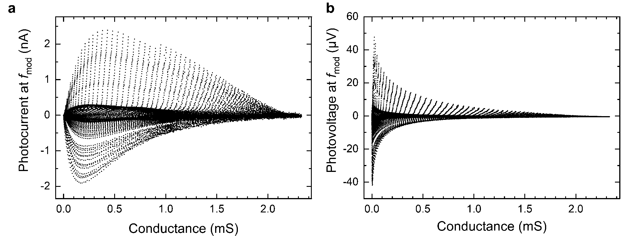
A key advantage of the two gates is the independent tuning of output impedance and responsivity. This enables impedance matching to external circuitry – a capability which is inherently built-in in the device design. The target working point for a desired photocurrent response and output impedance, i.e. the two gate voltages, is to be determined from the intersection of equi-photocurrent contours in Fig. 3 (b) with equi-conductance contours in Fig. 3 (a). This also means that detection sensitivity can be switched on or off with the gate voltages, while maintaining the device’s impedance, thus making it appear the same in the external circuit. The available responsivity and output impedance ranges can be found in Fig. 5.
2.4 Theory
We consider a narrow 2DEG under two semi-infinite gates. The gate voltages and induce a step-like potential , see Fig. 1. Under THz irradiation, an additional time-dependent potential is added to . is the amplitude of the THz electric field in x-direction acting on the 2DEG at the step, and the potential difference it induces. Electrons are assumed to pass the gap between the antenna wings ballistically, i.e. to have a mean free path exceeding µm (this condition is satisfied in the experiment). In the y-direction, an infinite potential well of width is assumed ( µm, see Methods), so that the ground-state energy of the transverse motion is µeV.
To describe the photoresponse of the system, we solve the time-dependent Schrödinger equation in the first-order perturbation theory, treating as a perturbation, see Methods. The resulting expression for the photocurrent is
| (1) |
The photocurrent’s dependence on the chemical potentials is described by a universal dimensionless function that depends on the two dimensionless parameters and and is antisymmetric, see Fig. 3 (d). The gates are pinched off at . In the area with and , where there are no electrons in both parts of the sample, the photocurrent vanishes. When only one of the chemical potentials is negative, down to , the function is non-zero: photoexcited electrons are still able to jump onto the step when .
The maximum of the function equals and is located at ; . Notably, this corresponds to the open regime far away from pinch-off, where in both parts of the system, and , electrons form a degenerate Fermi gas with chemical potentials well above the conduction band edges, as illustrated in Fig. 1 (b). This relationship between the radiation frequency and the chemical potentials allows to determine the optimal frequency range of the detection mechanism. Since typical electron concentrations in 2DEGs range from /cm2 [42] to /cm2 [43], optimal photodetection can be achieved between 0.15 – 20 THz. The in-plane photoelectric effect is thus ideally suited for detection of radiation in the entire THz range.
In Fig. 3 (f) we plot the (time-averaged) theoretical photocurrent expected under the experimental conditions, using the relationship between chemical potentials and gate voltages as described in the Methods section. There is a good qualitative agreement with the experimental photocurrent for V in Fig. 3 (e). In this regime the measured photocurrent peaks at in Fig. 3 (e), with a channel resistance of 3.7 k\textOmega. The position of maximum theoretical photocurrent in Fig. 3 (f) is close to the experimental peak position. The match between theory and experiment is best when considering the top-left regions (where ). This is sensible since it corresponds to a barrier under the wide gate, which is a better approximation of a semi-infinite potential step as considered in the theory, than the 200 nm narrow gate. In spite of the simplicity of the model, all key features are thus reproduced. A better agreement between theory and experiment can be achieved by considering a more detailed model of the potential, also taking into account the ungated region between the wide and narrow gates.
The strong increase in photocurrent under maximum asymmetry in the top-left and bottom-right regions in Fig. 3 (b), which is not covered in the theoretical framework, is likely related to an effect of the device geometry, such as a widening of the conducting channel, since edge depletion effects start to diminish at strongly positive gate voltages. An increase in channel width, which is µm in equilibrium as indicated in Fig. 2 (b), would give rise to an increased conductance in Fig. 3 (a), as the bottleneck in the form of the narrow channel is widened, and also to an enhanced photocurrent , which increases with the channel width.
Quantitatively, the theoretically calculated photocurrent of nA exceeds the experimentally measured value. This is in contrast to other possible interpretations, discussed in the next section, which predict a lower value than measured. The experimental photocurrent in the region V, Fig. 3 (e) is nA, and the overall maximum measured photocurrent is nA, Fig. 3 (b). This indicates that the experimentally observed signal can be further increased by optimizing the device design to reduce channel and contact resistances which diminish the measured current.
2.5 Discussion
We now check whether other detection mechanisms could explain the observed effect. Bolometric mechanisms commonly give rise to photoconductance, rather than a zero-bias photocurrent or -voltage [20, 27, 31], and dominate in the pinch-off regime, where conduction is sensitive to small temperature changes [27]. In contrast, in our case, the photocurrent is maximal in the open regime. In the case of a broken symmetry, a photocurrent may be observed, e. g. as a (photo-)thermoelectric effect [19]. However, the prerequisite for the applicability of such interpretations is local electron thermalisation. But in our case, the mean free path of electrons is very large: 20 µm in the wafer material, and even considering a reduction of within the channel due to the edge roughness, it still exceeds µm, the distance between the gates, which is the relevant length scale. Thus, electrons pass the region between the gates ballistically. This rules out local electron thermalisation, and mechanisms relying on it.
On the other hand, electron “heating” can also occur in a collisionless way, in the sense that the incident radiation increases the mean electron energy, as in Ref. [31]. The increase in the mean energy of the electrons can be estimated as µeV, which is a negligible amount (for the maximum electric field in x-direction of V/cm during a THz pulse with intensity , extracted from numerical simulations of the antenna amplification).
Another mechanism to consider is photon-assisted tunneling [24, 38, 33]: photons incident on a thin barrier in the tunneling regime can give rise to photoconductance. However in the present experiment, the size of the barriers created by the gates is macroscopically large ( µm in the case of the wide gate), and the photocurrent dominates in the open regime, with a degenerate electron gas. This rules out tunneling-related effects such as photon-assisted tunneling.
On the other hand, photon-assisted tunneling across a thin barrier can be understood as the difference of two photocurrents generated at the two edges of the barrier, which is considered as two mirrored potential steps. The total photocurrent will vanish at zero bias due to the inherent symmetry of the barrier, and a photoresponse will only be observed if the symmetry is intentionally broken by an applied voltage across the barrier. This explains why the photoresponse of thin tunneling systems such as quantum point contacts presents itself predominantly as photoconductance [27, 31, 33], rather than zero-bias photocurrent or photovoltage [20]. In our device, the translation symmetry is broken by the gate-induced potential step without any external source-drain bias, which is advantageous for noise performance. We implement the potential step using a macroscopically wide barrier and irradiate it on one side only. Thus we recover the giant photocurrent signal that tends to remain hidden in quantum point contacts.
Many THz detection experiments [25, 26, 44, 28, 29, 45, 30, 34, 35] were interpreted in terms of the plasma-wave mixing theory [37], a mechanism which at lower frequencies corresponds to distributed resistive mixing or resistive self-mixing [44, 45]. Let us estimate the absolute value predicted by the plasmonic mixing mechanism. In our experiment, the THz gate-to-channel voltage amplitude equals 0.18 mV for the average incident power according to numerical antenna simulations. The sample can be modelled as a back-to-back series connection of two 2DEGs with different densities. The source-drain distance is much longer than the plasmon decay length, and . Under these conditions, the plasmonic mixing theory [37] predicts a photovoltage of 0.2 µV at the point of maximum experimental photocurrent in the V area, , where the measured photovoltage is 1.8 µV, i. e. considerably higher. Furthermore, the maximum possible photovoltage for non-resonant detection is µV, according to Ref. [26], with in GaAs based FETs at low temperatures [26]. This is smaller than the experimental photovoltage of 5.6 µV in the area V, and more than an order of magnitude smaller than the maximal DC photovoltage of 56 µV at strong gate asymmetry as seen in Fig. 3 (a). In addition, even the qualitative form of the photoresponse cannot be explained: plasmonic mixing would result in a monotonous increase of the photocurrent the further apart the gate voltages are, and the broad maximum of the photocurrent observed experimentally would not be reproduced. Thus, other possible interpretations, as discussed above, cannot explain the effect.
In conclusion, we have demonstrated a fundamental physical phenomenon – the in-plane photoelectric effect. It has a number of advantages as compared to the conventional photoelectric effect. It is a purely quantum-mechanical, scattering-free phenomenon which has no intrinsic response time limit. The maximum photocurrent is obtained when the chemical potential lies above the potential step in both parts of the 2DEG, i.e., the 2DEG is well conducting. Such a situation has not been implemented so far, and would not work in a 3D case. No dc source-drain bias is required, whereas in 3D photoemissive detectors usually a bias is applied to extract the electrons. The effect is more than 10 times stronger than any mechanism previously considered in 2D electron systems. The potential step is artificially created and tunable by gate voltages; in contrast, in 3D photoemissive systems the workfunction is fixed by the material parameters. The effect is ideally suited for utilization across the whole THz range. As an inherent effect of 2D systems, it can be utilized in 2DEGs on the basis of III-V materials, silicon, as well as the novel 2D layered, graphene-related materials.
The detection principle based on the discovered phenomenon paves the way to a new class of photo-electric tunable-step (PETS) THz detectors. The presence of two gates allows independent tuning of output impedance and responsivity of the device, which facilitates integration into external circuits. The dual-gated, antenna-coupled device architecture will advance the development of fast and large-scale integrated THz detectors and focal plane arrays. Integrating PETS detectors with quantum cascade lasers, as is commonly done with photodiodes and optical laser chips, will be a valuable advancement towards market-ready THz QCL-based emitters.
3 Methods
3.1 Sample fabrication
The heterostructure used was deposited on a GaAs semi-insulating substrate. The sequence grown by molecular beam epitaxy was, after a 1 µm undoped GaAs buffer layer, 40 nm undoped Al0.33Ga0.67As; 40 nm n-doped Al0.33Ga0.67As with /cm3 doping density of Si donors; 10 nm GaAs cap. To process the sample, electron beam lithography is used to define an etch mask using ma-N 2410 resist onto the as-grown wafer. At this stage, the sample is etched to form a 100 nm high mesa with the narrow channel and areas for contact pads. The Ohmic source and drain contacts to the channel are processed using optical lithography by annealing an AuGeNi eutectic alloy. Next, electron beam lithography with poly(methyl methacrylate) resist is used to define a TiAu gate structure on top of the device which creates a bow-tie antenna that focuses the radiation to the channel. Optical lithography is used for creation of large-area TiAu bond pads. Finally, the sample is encapsulated in Shipley S1805 resist for surface protection.
3.2 Edge depletion
The lithographically defined channel width is 2.0 µm. Calibration of the mesa etching has shown that sideways etching of 165 nm occurs on average on either side of the mesa, so the actual mesa width is approximately 1.67 µm. Measurements on other samples created by this process have shown that the lateral edge depletion of the 2DEG is between 0.34 µm and 0.58 µm. Taking this into account, the actual width of the 2DEG in the channel, is between and µm, and is assumed to be 0.7 µm in the theory.
3.3 Electrical measurement setup
3.4 Determination of the power density at the sample
To illuminate the sample with THz radiation, we have constructed a setup coupling together two liquid helium continuous flow cryostats, one with a 1.9 THz single-plasmon QCL, and the other with the sample, using a copper waveguide. This waveguided setup allows quantitative determination of the THz intensity at the sample space. Before measurements, the QCL cryostat is first aligned so as to induce maximum photoresponse of the sample. After the measurements, the sample is warmed up and removed, while the QCL is kept lasing, and its temperature (18 K) and alignment are maintained. The total transmitted power at the sample space is then determined using a Thomas Keating absolute power meter, while the intensity distribution is measured using a Golay cell with a 1 mm aperture on a setup with motorised x, y scanning stages. We thus find the time-averaged intensity µW/mm2 at the sample space at the mode profile peak, where the intensity distribution reaches its maximum value.
3.5 Photocurrent calculation
The dynamics of photoexcited electrons is determined by the time-dependent Schrödinger equation:
| (2) |
In the transverse, y-direction we assume infinite potential walls at and , which gives quantization energies of , where µeV and is the subband index.
Solving Eq. (2) with as perturbation, we calculate the wavefunctions in zero and first order, and from them, the particle flows , and , . Here, is the flow of particles with energy incident onto the step from the right, and is the flow of particles with energy having passed the step and moving to the left (the definitions for “” are similar). Their ratio leads to the first-order transmission coefficients of particles having absorbed a THz quantum , defined as for positive, and for negative -direction of motion. Thus calculated transmission coefficients can be written in the form where and the functions are illustrated in Fig. 1 (c) for meV, meV, and meV. As seen from the plot, for all energies provided that , i. e. the particles flow onto the step. The photocurrent is then calculated as
| (3) |
where the factors containing the Fermi distribution function take into account the occupation of electron states and is the chemical potential of the unbiased system. Eq. (1) is obtained from Eq. (3) at temperature .
The perturbation theory parameter should be for the applicability of the theory. With the incident intensity of during a THz pulse, the electric field in x-direction acting on the 2DEG between the gates is V/cm according to the numerical antenna simulations in Comsol Multiphysics. This gives meV and , which justifies the perturbative approach and neglection of higher-order contributions to the photocurrent.
In order to transform the dependencies on chemical potentials in Eq. (1) and Fig. 3 (d) into gate voltage dependencies as shown in Fig. 3 (f), the connection between external gate potentials , and chemical potentials , is required. This relationship can be obtained from the Poisson equation, taking into account the screening of the external potential created by the gates,
| (4) |
and analogously, for and . Here is the equilibrium chemical potential, the equilibrium 2D electron density, and the effective Bohr radius in GaAs.
4 Acknowledgements
W.M. thanks the George and Lilian Schiff Studentship of the University of Cambridge for financial support and is grateful for the Honorary Vice-Chancellor’s Award of the Cambridge Trust. S.A.M. acknowledges funding from the European Union’s Horizon 2020 research and innovation programme Graphene Core 3 under Grant Agreement No. 881603. R.D. acknowledges support from the EPSRC (Grant No. EP/S019383/1). The authors acknowledge EPSRC funding within the Hyperterahertz grant, number EP/P021859/1, and thank Binbin Wei, Yuqing Wu, Ateeq Nasir, Ben Ramsay, and Antonio Rubino for helpful advice, as well as Abbie Lowe and Jonathan Griffiths for help with electron beam lithography. The authors express special thanks to Joanna Waldie for advice on sample fabrication and measurements and comments on the manuscript.
5 Author information
5.1 Contributions
W.M. conceived the device concept, designed, simulated, fabricated, and measured the samples, built the waveguide-coupled terahertz setup and wrote the paper. P.S. advised on instrumental techniques, helped and supported in the lab. N.W.A. built the motorised Golay cell scanning setup. S.J.K. advised on Comsol numerical simulations. R.W. advised on terahertz measurement techniques. T.A.M. did the lithographic electron beam exposure. R.D. participated in discussions of experimental findings. S.A.M. provided quantitative theory and corresponding contribution to the paper. H.E.B. grew the wafer material and advised. D.A.R. enabled and supervised the research and advised. All authors discussed the results and the manuscript.
5.2 Corresponding author
Correspondence to W. Michailow (wm297@cam.ac.uk).
References
- [1] Philipp Lenard “Über die lichtelektrische Wirkung” In Annalen der Physik 313.5 Wiley Online Library, 1902, pp. 149–198 URL: https://onlinelibrary.wiley.com/doi/pdf/10.1002/andp.19023130510
- [2] Albert Einstein “Über einen die Erzeugung und Verwandlung des Lichtes betreffenden heuristischen Gesichtspunkt” In Annalen der Physik 322.6 Wiley Online Library, 1905, pp. 132–148 DOI: 10.1002/andp.19053220607
- [3] Carl Neil Berglund and William Edward Spicer “Photoemission studies of copper and silver: theory” In Physical Review 136.4A APS, 1964, pp. A1030 URL: https://journals.aps.org/pr/abstract/10.1103/PhysRev.136.A1030
- [4] RM Broudy “Vectorial photoelectric effect” In Physical Review B 3.11 APS, 1971, pp. 3641 URL: https://journals.aps.org/prb/abstract/10.1103/PhysRevB.3.3641
- [5] JK Sass “Evidence for an anisotropic volume photoelectric effect in polycrystalline nearly free electron metals” In Surface Science 51.1 Elsevier, 1975, pp. 199–212 URL: https://www.sciencedirect.com/science/article/pii/0039602875902435
- [6] JP Girardeau-Montaut, C Girardeau-Montaut, SD Moustaizis and C Fotakis “Dependence of femtosecond single-photon photoemission from gold on laser beam incidence and polarization” In Applied Physics Letters 63.5 American Institute of Physics, 1993, pp. 699–701 URL: https://aip.scitation.org/doi/pdf/10.1063/1.109933
- [7] Gerald Hechenblaikner and Tobias Ziegler “The vectorial photoelectric effect under solar irradiance and its application to sun sensing” In Measurement Science and Technology 25.7 IOP Publishing, 2014, pp. 075103 URL: https://iopscience.iop.org/article/10.1088/0957-0233/25/7/075103/meta
- [8] AGU Perera, RE Sherriff, MH Francombe and RP Devaty “Far infrared photoelectric thresholds of extrinsic semiconductor photocathodes” In Applied Physics Letters 60.25 American Institute of Physics, 1992, pp. 3168–3170 DOI: 10.1063/1.106731
- [9] AGU Perera, HX Yuan and MH Francombe “Homojunction internal photoemission far-infrared detectors: photoresponse performance analysis” In Journal of Applied Physics 77.2 American Institute of Physics, 1995, pp. 915–924 URL: https://aip.scitation.org/doi/abs/10.1063/1.359019
- [10] WZ Shen “Recent Progress in Mid-and Far-Infrared Semiconductor Detectors” In International Journal of Infrared and Millimeter Waves 21.11 Springer, 2000, pp. 1739–1746 URL: https://link.springer.com/article/10.1023/A:1006758500042
- [11] Yan-Feng Lao, AG Unil Perera, LH Li, SP Khanna, EH Linfield and HC Liu “Tunable hot-carrier photodetection beyond the bandgap spectral limit” In Nature Photonics 8.5 Nature Publishing Group, 2014, pp. 412–418 URL: https://www.nature.com/articles/nphoton.2014.80
- [12] SG Matsik, MBM Rinzan, AGU Perera, HC Liu, ZR Wasilewski and M Buchanan “Cutoff tailorability of heterojunction terahertz detectors” In Applied Physics Letters 82.1 American Institute of Physics, 2003, pp. 139–141 URL: https://aip.scitation.org/doi/abstract/10.1063/1.1534409
- [13] AGU Perera, G Ariyawansa, PVV Jayaweera, SG Matsik, M Buchanan and HC Liu “Semiconductor terahertz detectors and absorption enhancement using plasmons” In Microelectronics Journal 39.3-4 Elsevier, 2008, pp. 601–606 URL: https://www.sciencedirect.com/science/article/pii/S002626920700198X
- [14] Peng Bai, YH Zhang, XG Guo, ZL Fu, JC Cao and WZ Shen “Realization of the high-performance THz GaAs homojunction detector below the frequency of Reststrahlen band” In Applied Physics Letters 113.24 AIP Publishing LLC, 2018, pp. 241102 URL: https://aip.scitation.org/doi/full/10.1063/1.5061696
- [15] Wen-Zhong Shen, AGU Perera, Hui-Chun Liu, M Buchanan and WJ Schaff “Bias effects in high performance GaAs homojunction far-infrared detectors” In Applied Physics Letters 71.18 American Institute of Physics, 1997, pp. 2677–2679 URL: https://aip.scitation.org/doi/abs/10.1063/1.120176
- [16] EE Haller, MR Hueschen and PL Richards “Ge:Ga photoconductors in low infrared backgrounds” In Applied Physics Letters 34.8 American Institute of Physics, 1979, pp. 495–497 URL: https://aip.scitation.org/doi/abs/10.1063/1.90861
- [17] GJ Stacey, JW Beeman, EE Haller, N Geis, A Poglitsch and M Rumitz “Stressed and unstressed Ge:Ga detector arrays for airborne astronomy” In International Journal of Infrared and Millimeter Waves 13.11 Springer, 1992, pp. 1689–1707 URL: https://link.springer.com/content/pdf/10.1007/BF01010739.pdf
- [18] H Zalinge, RW Heijden, JH Wolter, B Özyilmaz, A Böhm and P Wyder “Lateral photoelectric effect studies of a two-dimensional electron gas under quantum Hall conditions” In Semiconductor Science and Technology 19.9 IOP Publishing, 2004, pp. 1153
- [19] LW Molenkamp, H Van Houten, CWJ Beenakker, R Eppenga and CT Foxon “Quantum oscillations in the transverse voltage of a channel in the nonlinear transport regime” In Physical Review Letters 65.8 APS, 1990, pp. 1052
- [20] TJBM Janssen, JC Maan, J Singleton, NK Patel, M Pepper, JEF Frost, DA Ritchie and GAC Jones “A new mechanism for high-frequency rectification in a ballistic quantum point contact” In Journal of Physics: Condensed Matter 6.13 IOP Publishing, 1994, pp. L163 URL: https://iopscience.iop.org/article/10.1088/0953-8984/6/13/002/pdf
- [21] LP Kouwenhoven, S Jauhar, K McCormick, D Dixon, PL McEuen, Yu V Nazarov, NC Van Der Vaart and CT Foxon “Photon-assisted tunneling through a quantum dot” In Physical Review B 50.3 APS, 1994, pp. 2019 URL: https://journals.aps.org/prb/pdf/10.1103/PhysRevB.50.2019
- [22] LP Kouwenhoven, S Jauhar, J Orenstein, PL McEuen, Y Nagamune, J Motohisa and H Sakaki “Observation of photon-assisted tunneling through a quantum dot” In Physical Review Letters 73.25 APS, 1994, pp. 3443 URL: https://journals.aps.org/prl/pdf/10.1103/PhysRevLett.73.3443
- [23] H Drexler, JS Scott, SJ Allen, KL Campman and AC Gossard “Photon-assisted tunneling in a resonant tunneling diode: Stimulated emission and absorption in the THz range” In Applied Physics Letters 67.19 American Institute of Physics, 1995, pp. 2816–2818 URL: https://aip.scitation.org/doi/pdf/10.1063/1.114794
- [24] S Verghese, RA Wyss, Th Schäpers, A Förster, MJ Rooks and Qing Hu “Photon-assisted transport through quantized energy states in a lateral dual-gate device” In Physical Review B 52.20 APS, 1995, pp. 14834 URL: https://journals.aps.org/prb/pdf/10.1103/PhysRevB.52.14834
- [25] Jian-Qiang Lü, Michael S Shur, Jeffrey L Hesler, Liangquan Sun and Robert Weikle “Terahertz detector utilizing two-dimensional electronic fluid” In IEEE Electron Device Letters 19.10 IEEE, 1998, pp. 373–375 URL: https://ieeexplore.ieee.org/document/720190/
- [26] W. Knap, V. Kachorovskii, Y. Deng, S. Rumyantsev, J.-Q. Lü, R. Gaska, M.. Shur, G. Simin, X. Hu, M. Khan, C.. Saylor and L.. Brunel “Nonresonant detection of terahertz radiation in field effect transistors” In Journal of Applied Physics 91.11 AIP, 2002, pp. 9346–9353 URL: https://aip.scitation.org/doi/abs/10.1063/1.1468257
- [27] JW Song, GR Aizin, J Mikalopas, Y Kawano, K Ishibashi, N Aoki, JL Reno, Y Ochiai and JP Bird “Bolometric terahertz detection in pinched-off quantum point contacts” In Applied Physics Letters 97.8 American Institute of Physics, 2010, pp. 083109 URL: https://aip.scitation.org/doi/pdf/10.1063/1.3475488
- [28] S Nadar, H Videlier, Dominique Coquillat, Frederic Teppe, M Sakowicz, N Dyakonova, Wojciech Knap, D Seliuta, I Kašalynas and G Valušis “Room temperature imaging at 1.63 and 2.54 THz with field effect transistor detectors” In Journal of Applied Physics 108.5 AIP, 2010, pp. 054508 URL: https://aip.scitation.org/doi/10.1063/1.3463414
- [29] Wojciech Knap, Salman Nadar, Hadley Videlier, Stephane Boubanga-Tombet, Dominique Coquillat, Nina Dyakonova, Frederic Teppe, Kristoph Karpierz, Jerzy Łusakowski, Maciej Sakowicz, Irmantas Kasalynas, Dalius Seliuta, Gintaras Valusis, Taiichi Otsuji, Yahya Meziani, Abdel El Fatimy, Simon Vandenbrouk, Kamel Madjour, Didier Théron and Christophe Gaquière “Field effect transistors for terahertz detection and emission” In Journal of Infrared, Millimeter, and Terahertz Waves 32.5 Springer, 2011, pp. 618–628
- [30] Richard Al Hadi, Hani Sherry, Janusz Grzyb, Yan Zhao, Wolfgang Forster, Hans M Keller, Andreia Cathelin, Andreas Kaiser and Ullrich R Pfeiffer “A 1 k-pixel video camera for 0.7–1.1 terahertz imaging applications in 65-nm CMOS” In IEEE Journal of Solid-State Circuits 47.12 IEEE, 2012, pp. 2999–3012 URL: https://ieeexplore.ieee.org/document/6363486/
- [31] A D Levin, G M Gusev, Z D Kvon, A K Bakarov, N A Savostianova, S A Mikhailov, E E Rodyakina and A V Latyshev “Giant microwave photo-conductance of a tunnel point contact with a bridged gate” In Applied Physics Letters 107.7 AIP Publishing, 2015, pp. 072112 URL: https://aip.scitation.org/doi/abs/10.1063/1.4928733
- [32] Taiichi Otsuji “Trends in the research of modern terahertz detectors: plasmon detectors” In IEEE Transactions on Terahertz Science and Technology 5.6 IEEE, 2015, pp. 1110–1120
- [33] M Otteneder, ZD Kvon, OA Tkachenko, VA Tkachenko, AS Jaroshevich, EE Rodyakina, AV Latyshev and SD Ganichev “Giant Terahertz Photoconductance of Quantum Point Contacts in the Tunneling Regime” In Physical Review Applied 10.1 APS, 2018, pp. 014015
- [34] Audrey Zak, Michael A Andersson, Maris Bauer, Jonas Matukas, Alvydas Lisauskas, Hartmut G Roskos and Jan Stake “Antenna-integrated 0.6 THz FET direct detectors based on CVD graphene” In Nano Letters 14.10 ACS Publications, 2014, pp. 5834–5838 URL: https://pubs.acs.org/doi/abs/10.1021/nl5027309
- [35] Leonardo Viti, Jin Hu, Dominique Coquillat, Antonio Politano, Christophe Consejo, Wojciech Knap and Miriam S Vitiello “Heterostructured hBN-BP-hBN Nanodetectors at Terahertz Frequencies” In Advanced Materials 28.34 Wiley Online Library, 2016, pp. 7390–7396 URL: https://onlinelibrary.wiley.com/doi/abs/10.1002/adma.201601736
- [36] Riccardo Degl’Innocenti, Long Xiao, David S. Jessop, Stephen J. Kindness, Yuan Ren, Hungyen Lin, J. Zeitler, Jack A. Alexander-Webber, Hannah J. Joyce, Philipp Braeuninger-Weimer, Stephan Hofmann, Harvey E. Beere and David A. Ritchie “Fast Room-Temperature Detection of Terahertz Quantum Cascade Lasers with Graphene-Loaded Bow-Tie Plasmonic Antenna Arrays” In ACS Photonics 3.10, 2016, pp. 1747–1753 DOI: 10.1021/acsphotonics.6b00405
- [37] Mikhail Dyakonov and Michael Shur “Detection, mixing, and frequency multiplication of terahertz radiation by two-dimensional electronic fluid” In IEEE Transactions on Electron Devices 43.3 IEEE, 1996, pp. 380–387 URL: https://ieeexplore.ieee.org/document/485650/
- [38] Olga Aleksandrovna Tkachenko, Vitalii Anatol’evich Tkachenko and Ze Don Kvon “Photon-assisted electron transport through a quantum point contact in a microwave field” In JETP Letters 102.6 Springer, 2015, pp. 378–382
- [39] Jerome Faist, Federico Capasso, Deborah L Sivco, Carlo Sirtori, Albert L Hutchinson and Alfred Y Cho “Quantum cascade laser” In Science 264.5158 American Association for the Advancement of Science, 1994, pp. 553–556 URL: http://science.sciencemag.org/content/sci/264/5158/553.full.pdf
- [40] Rüdeger Köhler, Alessandro Tredicucci, Fabio Beltram, Harvey E Beere, Edmund H Linfield, A Giles Davies, David A Ritchie, Rita C Iotti and Fausto Rossi “Terahertz semiconductor-heterostructure laser.” In Nature 417, 2002, pp. 156–159 DOI: 10.1038/417156a
- [41] JS Blakemore “Semiconducting and other major properties of gallium arsenide” In Journal of Applied Physics 53.10 AIP, 1982, pp. R123–R181 URL: https://aip.scitation.org/doi/abs/10.1063/1.331665
- [42] Y Hirayama, K Muraki and T Saku “Two-dimensional electron gas formed in a back-gated undoped heterostructure” In Applied Physics Letters 72.14 American Institute of Physics, 1998, pp. 1745–1747 URL: https://aip.scitation.org/doi/abstract/10.1063/1.121171
- [43] VG Mokerov, Yu V Fedorov and AV Hook “High density 2DEG in III-V semiconductor heterostructures and high-electron-mobility transistors based on them” In Semiconductors 33.9 Springer, 1999, pp. 970–971 URL: https://link.springer.com/article/10.1134/1.1187814
- [44] Alvydas Lisauskas, Ullrich Pfeiffer, Erik Öjefors, Peter Haring Bolìvar, Diana Glaab and Hartmut G Roskos “Rational design of high-responsivity detectors of terahertz radiation based on distributed self-mixing in silicon field-effect transistors” In Journal of Applied Physics 105.11 AIP, 2009, pp. 114511 URL: https://aip.scitation.org/doi/abs/10.1063/1.3140611
- [45] Sebastian Boppel, Alvydas Lisauskas, Martin Mundt, Dalius Seliuta, Linas Minkevicius, Irmantas Kasalynas, Gintaras Valusis, Martin Mittendorff, Stephan Winnerl, Viktor Krozer and Hartmut G Roskos “CMOS integrated antenna-coupled field-effect transistors for the detection of radiation from 0.2 to 4.3 THz” In IEEE Transactions on Microwave Theory and Techniques 60.12 IEEE, 2012, pp. 3834–3843 URL: https://ieeexplore.ieee.org/document/6353608/