∎
Indian Institute of Technology Hyderabad, Kandi, Sangareddy, Telangana, 502285, India
22email: ph17resch11011@iith.ac.in 33institutetext: J. Arout Chelvane 44institutetext: Defence Metallurgical Research Laboratory, Hyderabad, 500058, India
44email: aroutchelvane@gmail.com 55institutetext: J. Mohanty 66institutetext: Nanomagnetism and Microscopy Laboratory, Department of Physics
Indian Institute of Technology Hyderabad, Kandi, Sangareddy, Telangana, 502285, India
66email: jmohanty@phy.iith.ac.in
Effect of Ti underlayer thickness on the magnetic anisotropy of TbFe thin films
Abstract
In this study, we address the impact of Ti underlayer thickness (UL: 0-40 nm) on the structural, magnetic, and microscopic properties of TbFe thin films. The structural analysis confirmed the intermixing at interfaces of the Ti and TbFe layer with the increment of UL thicknesses. Out-of-plane (OOP) coercivity (), and saturation field () gradually increased with an increase in UL thickness regardless of interface mixing. For UL = 10 nm, the domain contrast and OOP stray field strength were enhanced, which may be due to the extent of - hybridization dominated over the influence of interfacial roughness. While for UL = 20, and 40 nm, the extent of interfacial roughness dominated the hybridization effects and as a result, stray fields deteriorated. By placing UL of 20 nm, increased by nearly 6 times more than the bare TbFe system. So, we observe a state with high OOP combined with nearly zero OOP stray fields that are found to co-exist in the sample. The magnetization reversal studies on a large area reveal domain nucleation followed by domain-wall motion in all the films. The idea of tuning magnetic properties by varying thicknesses of Ti UL may useful in spintronics applications.
Keywords:
Perpendicular magnetic anisotropy X-ray reflectivity TbFe ferrimagnetism Magnetic domains Ti underlayer Domain reversals1 Introduction
The improvement of magnetic properties of thin films associated with perpendicular magnetic anisotropy (PMA) system has been emphasized, for many decades, due to the possible industrial applications like high-density perpendicular recording media, magnetic tunnel junctions, sensors, etc. The PMA systems like CoPt, FePt alloys are crystalline, therefore tuning of PMA can be studied by understanding the magneto-crystalline anisotropy in the system CoPt ; FePt ; FePt_cap . However, the theory behind PMA in amorphous systems like rare-earth transition-metal (RE-TM), CoFeB, CoCrPt, is still elusive till date GdFe_amor ; TbFe_amor ; CoFeB_amor ; CoCrPt_amor . The PMA in these systems can be developed by simply varying thickness, strain-modulation, and interface inducing roughness in the film, etc. Several approaches have been considered for further improvement in PMA property, by deposition of a suitable underlayer (UL) or seed-layer, incremental in the repetition of multilayers (ML), inducing more interfacial roughness, etc.
Literature suggests various UL like Ti, V, Cr, Ni, Cu, Ta, Pd, etc. have been tested on various films like FeCo, FePt, CoCrPt, CoCr, FePt ML, etc. For example, Ti UL was used to improve the degree of order of FePt films FePt , to improve the PMA property of CoCrPt CoCrPt_amor and CoCr CoCr films. Interestingly it was observed that Ti and Ta UL made considerable improvement in magnetic properties of FeCo films compared to other UL FeCo . This may be due to the development of grain size and the internal stress of the film. Another important thing is, Ti UL also minimizes the contact resistance of single-wall-nano-tube and a metal electrode which can be beneficial for various electrical applications SWDW .
RE-TM films exhibit an impressive PMA property suitable for possible spintronics applications. GdFe GdFe_amor , TbFe TbFe_amor , GdFeCo GdFeCo many more systems were investigated on the light of their thickness, composition, and various UL to enhance PMA property. This tuning of properties depends strictly on the thickness of the film and interface properties. When the film thickness nm, interface-driven properties or effects become dominant. However, for nm volume thickness shows an effective bulk-like property, whereas interface effects become negligible. These bulk properties are mostly observed in the amorphous system irrespective of the sample preparation technique.
Here, we have chosen an amorphous ferrimagnetic TbFe system with various thicknesses of Ti UL to observe a full extent of variance in structural, magnetic, and microscopic properties. First, we observed TbFe of 40 nm thickness gives a clear PMA sign with nice stripe magnetic domains. Then, we varied the Ti layer of various thicknesses (10, 20, and 40 nm) to observe the effect of interface roughness, pinning sites, and hybridization effects of the films towards structural, magnetic, and microscopic phenomena. Here, we observed higher OOP values along with nearly null OOP stray fields in UL of 20 nm and 40 nm sample. This observation is quite new in these kinds of bulk PMA system, as of our knowledge.
2 Experimental detail
Si / Ti() / TbFe(40 nm) / Cr(3 nm); with = 0, 10, 20, and 40 nm thin films were prepared by electron beam evaporation technique. Cr (3 nm) was used as a capping layer to protect the film from oxidation, while Ti is used as UL. Films were deposited with a rate of deposition Å/sec. Tb-Fe films were deposited from its composite alloy, after deposition the composition of the film was estimated by energy dispersive spectroscopy (EDS) analysis. For = 0 nm can be noted as a bare TbFe film of 40 nm, which means TbFe film does not have any UL influence. The background pressure was maintained at around during deposition. To understand the effect of various thicknesses of UL on structural formations grazing incident X-ray diffraction (GI-XRD), and the X-ray reflectivity (XRR) technique were used. Atomic force microscopy (AFM) was used for identifying the topographic information. Magnetic force microscopy (MFM) was used to probe the stray fields emanating from the film surface. For hysteresis and domain reversal studies, we have used polar magneto-optical Kerr microscopy (PMOKE) (spot size 3 m).
3 Results and discussions
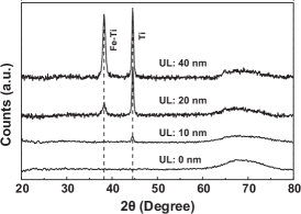
From EDS analysis (not presented here) composition of the film turns out to be for all the samples. Figure 1 represents GIXRD patterns of the Tb-Fe film with various UL thicknesses. Bare 40 nm thick TbFe film of shows an amorphous signature, which is consistent with amorphous nature of RE-TM RE_TM ; GdFe_amorphous ; TbFeCo_amorphous ; DyTbFeCo_amorphous ; TbFe_oPMA_amorphous . However, it is observed in akin GdFe films with the Gd composition less than 15 at. % are not amorphous, while more than 20 at. % shows an amorphous behavior GdFe_per_amor . Comparing with the literature database, in this case, Tb composition was estimated as 30 at. % for all the TbFe films, therefore it is expected to exhibit an amorphous nature in the as-deposited state. For UL of 10 nm, the film shows the hcp phase of Ti, which is at 44∘. Along with this, the Fe-Ti phase is observed in the case of UL = 20, and 40 nm. This means that the possibility of diffusion of Fe and Ti may occur at the interface of Ti-UL and TbFe film. The effect of this diffusion during the growth gets enhanced when UL thicknesses are increased which is also evident from the peak intensity. To further probe the individual layer thickness and rms roughness we implement a non-destructive XRR technique. Figure 2 (a) and 2 (b) represents XRR spectra and corresponding electron density profile (EDP) of various films respectively. Despite of being amorphous in the case of UL: 0 nm (observed by GIXRD), we observe Kiessig fringes in the corresponding reflectivity spectra because of the difference in electron density of TbFe and Cr layers. The extracted data of individual layer thickness (t), root mean square (rms) roughness (), and density () of the layer are summarized in Table 1. The composition of well agreed with the experimental spectra, which is also evident from EDS analysis earlier. Expected thickness of TbFe of nm and Cr of nm (UL: 0 nm) is found to be as nm and nm respectively from XRR analysis. Slight increment in inter-diffusion of the TbFe and Ti layer (formed as ) is observed for increase in UL thickness. Similar evidence of UL (Cu) diffusion into the RE-TM magnetic layer (Sm) is observed using the elemental map and energy dispersive x-ray spectroscopy line analysis underlayer_Cu . The increment of UL thickness has a significant impact on the microstructural, magnetic, and microscopic properties of the sample.
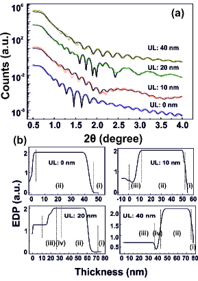
| Sample | Parameter | Ti | Cr | ||
|---|---|---|---|---|---|
| t () | - | - | 42.5 | 2.7 | |
| 0 nm | () | - | - | 1.2 | 1.1 |
| () | - | - | 8.42 | 6.04 | |
| t () | 7.9 | - | 42.9 | 2.5 | |
| 10 nm | () | 1.1 | - | 0.6 | 0.4 |
| () | 4.75 | - | 8.50 | 5.18 | |
| t () | 16.7 | 4.5 | 39.9 | 3.4 | |
| 20 nm | () | 1.5 | 1.4 | 1.7 | 1.3 |
| () | 4.37 | 6.35 | 8.43 | 2.73 | |
| t () | 34.2 | 5.9 | 34.2 | 2.4 | |
| 40 nm | () | 1.9 | 2.2 | 1.8 | 1.5 |
| () | 4.21 | 6.12 | 9.22 | 6.04 |
Ti UL affects the microscopic properties of the sample. Figure 3 shows AFM and MFM images of TbFe films grown with various thicknesses of Ti UL. AFM images revealed that the surface morphology slightly changed with increase in UL thickness. MFM images are found to be free from topographic influences. TbFe film (UL : 0 nm) shows a labyrinth-like stripe pattern as represented in fig. 3-(ii) (a). TbFe system also exhibits a honeycomb-like structure as reported in literature TbFe_honey . The yellow, and red colors represent up-, and down-magnetization respectively. The average domain width and contrast are enhanced for UL = 10 nm (fig. 3(ii) (b)). These domain-orientations are similar to the case of UL = 0 nm film. In a way, by placing a 10 nm Ti UL enhances the domain contrast and average domain size in the film. However, domain contrast becomes weaker for further increment in UL thickness. The yield in the electron beam evaporation technique is quite high, so, it is suspected that roughness may increase by increasing the thickness of the Ti UL. It is observed that the interface roughness (, Table 1), and surface roughness ( 0.89 nm, Table 2) of UL = 50 nm are comparatively higher than the lower UL thicknesses. XRR analysis (Table 1) also confirms increase in value due to increase in UL thickness. Further increment in UL thickness to 25 nm, stray fields (probing by MFM) that are emanating from the samples significantly deteriorates resulting in faint maze-like domains as shown in fig. 3-(ii) (c). For UL = 50 nm, a null out-of-plane contrast, which is observed in MFM image (fig. 3-(ii) (d)).
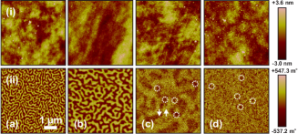
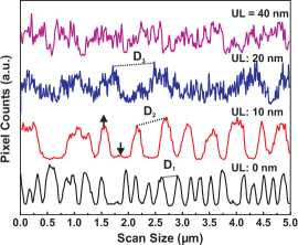
It was observed that microscopic properties are enhanced for UL thickness up to 10 nm. Further increment in UL thickness leads to deterioration of magnetic contrast probably due to the increase of interface-induced-roughness. The root-mean-squared surface roughness (), areal percentage (%) of up- and down-domains are summarized in Table 2. By increasing the thickness of Ti UL, is found to be increasing. Although can not significantly describe the details of interfacial roughness (), still it hints overall roughness of the sample. For UL = 0 nm, the area of down-domains (60 %) are more than up-domains (40 %). By increasing the UL thickness, % of down-domains are decreased compared to % of up-domains. Meanwhile, this is observed as UL thickness helped to increase the average-domain-size, and after a certain thickness, stray fields that are emanating from these domains become deteriorated. The domain sizes are extracted by taking a line scan over the MFM images (fig. 4). The sign of up- or down-domains are marked as up- or down-arrow in the line scan of UL = 10 nm. Domain size can be calculated by considering two neighboring domains, mentioned as , black dotted lines over the line scans. Keeping in mind, up to UL = 25 nm, we observed the appearance of domains. In the case of UL = 50 nm, we did not observe any domains.
As we observe various thicknesses of Ti UL fascinates the microscopic domain evolution of the system. So, the reversal mechanism of these magnetic films would be of fundamental interest. The magnetization reversals along with Kerr hysteresis are captured by using the PMOKE technique. MOKE can measure the change in rotation of polarization of incident light after reflected from the magnetized surface. Here, the Kerr rotation (KR) can be detected by even a small change of 5 . The MOKE effect is a relativistic quantum effect, which arises due to the combined effect of two central phenomena. One is corresponding to the inherent magnetization of the host sampleandother one is the spin-orbit interaction and the exchange interaction among host atoms. Generally speaking here, KR values can be considered as additional evidence of correlation of perpendicular moments in the system.
Figure 5-(i) represents MOKE measurements of 40 nm thick TbFe film. The Kerr hysteresis (Kerr signal vs Field) shows a nearly square hysteresis behavior. The and KR were recorded as 465 Oe and 185 respectively. This film is saturated at a field of 985 Oe. The magnetization reversal is observed to be initially dominated by nucleation then driven by domain wall motion. Similarly, we capture both Kerr loops and reversal domains for both UL = 10, 20 nm (fig. 5-(ii), (iii)). The , KR, and saturation field () values are summarized in the Table 2. Magnetization reversals of UL = 10, and 20 nm, are of similar nature to the case of bare TbFe 40 nm film. The reversal mechanism initially started from nucleation-dominated to wall-motion dominated one in all the cases.
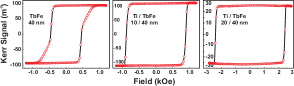
From Table 2, it is found that the increment of UL thickness results in gradual increase in OOP . This signifies magnetic moments are still lying perpendicular to the plane of the sample with increment in UL thickness. OOP of UL = 20 nm is 60 % more than in the case of UL = 10 nm. Whereas, strength of OOP stray field of UL = 20 nm is weakened compared to UL = 10 nm (fig. 3, and corresponding line scans in fig. 4). So, placing a UL ultimately enhance and values. A more understanding of the samples can be derived by considering KR values. We observe KR of UL = 10 nm (222 ) shows an improvement over UL = 0 nm (185 ) (refer Table 2). This shows a possible enhancement of correlation, and/or interaction of local magnetic moments, which is due to 10 nm of Ti UL. While in the case of UL = 20 nm, KR rapidly decreases to 51 . This may be due to magnetic moments are intermixed, and/or trapped within the proximity of interface roughness, which leads to a reduction of KR values as Kerr signals are only sensitive to magnetic moments. So, one can correlate these and KR values to the strength of perpendicular anisotropy.
| KR | |||||
| (nm) | (nm) | ( 5 %) | ( 5 Oe) | ( 5 Oe) | () |
| 0 | 0.50 | 40/60 | 465 | 985 | 185 |
| 10 | 0.60 | 48/52 | 890 | 1045 | 222 |
| 20 | 0.85 | 55/45 | 2410 | 2550 | 51 |
| 40 | 0.89 | – | – | – | – |
The enhancement or deterioration of magnetic and/or microscopic properties with the increment in thicknesses of Ti UL can be understood by following conclusive understanding. When a film gets deposited on the substrate, the system experiences lots of thermal stress, due to difference in thermal expansion coefficients between substrate and film, or between films, or mismatch lattice parameters between adjacent layers. In our case, also, bare amorphous Tb-Fe film of 40 nm experiences thermal stress, but the effect would be minimal due to given thickness. However, the origin of PMA is expected to be more prominent by - correlations TbFe_origin which leads to structural anisotropy in these kinds of amorphous system. In such a case, one can say that these films are more dominated by magneto-crystalline anisotropy, as PMA increases by increasing the thickness of the film GdFe_thickness . When we place Ti UL, Tb-Fe film grows on UL rather on the Si substrate, microscopic property changes. As Ti shows crystalline behavior (fig. 1), placing as UL will create a lattice mismatch between Ti and Tb-Fe layers, at the same time thermal stress on the TbFe layer reduces. However, these effects are not prominent in our case as the TbFe is inherently amorphous. In addition to this, there could be another phenomenon, hybridization, coexist between interface. It is not that 3d-magnetism leads to large exchange interactions (here, atoms) whereas 4f-magnetism drives large magneto-crystalline anisotropy (here, Tb atoms) 3d_4f . The extended length of the hybridization is more prominent in the ultrathin system, where interfacial roughness is very nominal. It is also observed that Ti () alloys show a faint-magnetic behavior when it is mixed with Fe, Co, or Ni (any strong magnetic material) Ti_book . Up to UL = 10 nm, we observe a nominal roughness 0.60 nm (Table 2). The reason for increment in domain size could be the lateral extent of hybridization of Fe () and Ti (), hybridization, become more prominent than the extent of interfacial roughness. As the thickness of UL increases, the extent of interfacial roughness gets dominated over hybridization effects, as a result, local anisotropy becomes weak and local moments may get trap in point-like defects present in the sample. These moments seem to be trapped by the proximity of interfacial roughness. One such observation was also found in an ultrathin TbCo system, 3 nm Ti_alloy_PMA . The reason for the enhancement of PMA was elucidated due to the appearance of a rugged interface.
The above understanding of magnetic and microscopic properties of TbFe films can be (a) by increasing UL thicknesses perpendicular anisotropy gradually increases regardless of interfacial roughness, (b) increment in UL thickness beyond a certain thickness leads to intermixing of magnetic moments with the proximity of interface roughness, while magnetic moments still lies perpendicular to the film plane. However strength of OOP stray fields are decreased. For instance, in UL = 20 nm case, one can observe with a considerable PMA (as is more) while OOP stray field is weakened. This contrast mixing properties due to the UL which is addressed in this study. Magnetometry measurements of UL = 40 nm has a similar range of value compared to that of UL = 20 nm.
4 Summary
In summary, we have investigated structural, microscopic, and magnetic properties of magnetic anisotropy in TbFe thin films by placing a wide range of Ti UL thickness. By increasing the thickness of UL which results in an increment in interfacial roughness with the formation of Fe-Ti phases. Here, we observed that (i) for UL = 10 nm, the possibility of extended - hybridization dominates over the influence of interfacial roughness, as a result, the strength of stray fields enhanced, (ii) for UL = 20 nm and 40 nm, the extent of interfacial roughness dominates over the hybridization effects as a result stray fields deteriorated. However, and are gradually increased with the increment of UL thickness. By placing UL of 20 nm, increases nearly 6 times more than the bare TbFe film, whereas Kerr rotation decreased by more than 4 times compared to UL of 10 nm. The magnetization reversal studies reveal domain nucleation followed by domain-wall motion in all the films.
References
- (1) Glemarie C. Hermosa and An-Cheng Sun, AIP Advances, 10(1),015132 (2020).
- (2) S.C. Chen, P.C. Kuo, S.T. Kuo, A.C. Sun, C.T. Lie, and C.Y. Chou, Mat. Sci. and Engg., 98(3), 244247 (2003).
- (3) X. Han, H. Cui, B. Liu, C. Tian, J. Wang, H. Chen, and H. Yuan, Sci. Rep., 8(9429), 112 (2018).
- (4) A. Talapatra, J. Arout Chelvane, and J. Mohanty, AIP Conf. Proc., 1832(1), 130044(2017).
- (5) S. Maneesh, J. Arout Chelvane, A. Talapatra, H. Basumatary, J. Mohanty, S.V. Kamat, J. Magn. Magn. Mater, 448, 31-37 (2018).
- (6) B. Cui, C. Song, Y. Y. Wang, W. S. Yan, F. Zeng, and F. Pan, J. Phys. Condens. Matter, 25(10), 106003 (2013).
- (7) C.J. Sun, G.M. Chow, E.W. Soo, J.P. Wang, Y.K. Hwu, T.S. Cho, J.H. Je, H.H. Lee, J.W. Kim, and D.Y. Noh, J. Nanosci. Nanotechnol, 1(3), 271-273 (2001).
- (8) O. Kitakami, K. Ojima, Y. Ogawa, T. Maro, and H. Fujiwara, IEEE Trans. Magn, 23(5), 2797-2799 (1987).
- (9) X. Liu, H. Kanda, and A. Morisako, Journal of Phys.: Conf. Series, 266(1), 012037 (2011).
- (10) S. Hwang, Y. Kim, H. Choi, M. Jeon, and S. Lee, Chinese Journal OF Phys., 49(5), 1102-1110 (2011).
- (11) M. Ding, and S. J. Poon, J. Magn. Magn. Mater, 339, 51-55 (2013).
- (12) G. Bihlmayer, Density‐functional Theory of Magnetism, Handbook of magnetism and advanced magnetic materials (2007).
- (13) S. Honda, M. Nawate, M. Ohkoshi, and T. Kusuda, J. Appl. Phys, 57(8), 1208-1215 (1985).
- (14) A. Chekanov, K. Matsumoto, and K. Ozaki, J. Appl. Phys, 90(9), 4657-4663 (2001).
- (15) J. Arout Chelvane, A. Sherly, M. Palit, A. Talapatra, and J. Mohanty, J Mater Sci: Mater Electron, 30(9), 8989-8995 (2019).
- (16) V. G. Harris, K. D. Aylesworth, B. N. Das, W. T. Elam, and N. C. Koon, Phys. Rev. Lett., 69(13), 1939 (1992).
- (17) Y. Mimura, N. Imamura, T. Kobayashi, A. Okada, and Y. Kushiro, J. Appl. Phys, 49(3), 1208-1215 (1978).
- (18) Y.K. Takahashi, T. Ohkubo, and K. Hono, J. Appl. Phys, 100,(5), 053913(2006).
- (19) Z. Sun, T. Zhu, Z. Zhang, B. Shen, B.Han, J. Shih, and T. Chin, J. Appl. Phys, 93(10), 8534-8536 (2003).
- (20) V. G. Harris, K. D. Aylesworth, B. N. Das, W. T. Elam, and N. C. Koon, Phys. Rev. Lett, 69(13), 1939 (1992).
- (21) A. Talapatra, J. Arout Chelvane, and J. Mohanty, AIP Conf. Proc, 1832(1), 130044 (2017).
- (22) L.T. Baczewski, D. Givord, J.M. Alameda, B. Dieny, J.P. Nozieres, J.P. Rebouillat, and J. J. Prejean, Acta Phys. Pol. A, 83, 629-629 (1993).
- (23) E.W. Collings, Applied Superconductivity, Metallurgy, and Physics of Titanium Alloys: Fundamentals Alloy Superconductors: Their Metallurgical, Physical, and Magnetic-Mixed-State Properties, Springer Science & Business Media (2013).
- (24) C.M. Lee, L.X. Ye, J.M. Lee, T.H. Hsieh, J.W. Syu, W.J. Chen, C.Y. Huang, and T.H. Wu, IEEE Trans. Magn, 45(10), 4023-4026 (2009).