Optical Modulation of Electron Beams in Free Space
Abstract
We exploit free-space interactions between electron beams and tailored light fields to imprint on-demand phase profiles on the electron wave functions. Through rigorous semiclassical theory involving a quantum description of the electrons, we show that monochromatic optical fields focused in vacuum can be used to correct electron beam aberrations and produce selected focal shapes. Stimulated elastic Compton scattering is exploited to imprint the phase, which is proportional to the integrated optical field intensity along the electron path and depends on the transverse beam position. The required light intensities are attainable in currently available ultrafast electron microscope setups, thus opening the field of free-space optical manipulation of electron beams.
I Introduction
Electron microscopy has experienced impressive advances over the last decades thanks to the design of sophisticated magnetostatic and electrostatic lenses that reduce electron optics aberrations Haider et al. (1998); Batson et al. (2002); Hawkes and Spence (2019) and are capable of focusing electron beams (e-beams) with subångstrom accuracy Nellist et al. (2004); Muller et al. (2008). In addition, the availability of more selective monochromators Krivanek et al. (2014) enable the exploration of sample excitations down to the mid-infrared regime Lagos et al. (2017); Hage et al. (2018, 2019); Hachtel et al. (2019). Such precise control over e-beam shape and energy is crucial for atomic-scale imaging and spectroscopy Haider et al. (1998); Batson et al. (2002); Hawkes and Spence (2019); Krivanek et al. (2014); Nellist et al. (2004); Muller et al. (2008); Lagos et al. (2017); Hage et al. (2018, 2019); Hachtel et al. (2019).
The focused e-beam profile ultimately depends on the phase acquired by the electron along its passage through the microscope column. Besides electron optics lenses, several physical elements have been demonstrated to control transverse e-beam shaping. In particular, biprisms based on biased wires provide a dramatic example of laterally-varying phase imprinting that is commonly used for e-beam splitting in electron holography Möllenstedt and Düker (1956), along with applications such as symmetry-selected plasmon excitation in metallic nanowires Guzzinati et al. (2017). In a related context, vortex e-beams have been realized using a magnetic pseudo-monopole Béché et al. (2014). Recently, plates with individually-biased perforations have been developed to enable position-selective control over the electric Aharonov-Bohm phase stamped on the electron wave function Verbeeck et al. (2018), while passive carved plates have been employed as amplitude filters to produce highly-chiral electron vortices Verbeeck et al. (2010); McMorran et al. (2011); Shiloh et al. (2014) and aberration correctors Grillo et al. (2017); Shiloh et al. (2018).
The electron phase can also be modified by the ponderomotive force associated with the interaction between e-beams and optical fields. In particular, periodic light standing waves were predicted to produce electron diffraction Kapitza and Dirac (1933), eventually observed in a challenging experiment Freimund et al. (2001); Freimund and Batelaan (2002); Batelaan (2007) that had to circumvent the weak free-space electron-photon coupling associated with energy-momentum mismatch García de Abajo (2010). Such mismatch forbids single photon emission or absorption processes by free electrons, consequently limiting electron-light coupling to second-order interactions that concatenate an even number of virtual photon events. This type of interaction has been recently exploited to produce attosecond free-electron pulses Koz’ak et al. (2018); Koz’ak (2019). Interestingly, the presence of material structures introduces scattered optical fields that can supply momentum and break the mismatch, thus enabling real photon processes García de Abajo (2010), used for example in laser-driven electron accelerators Black et al. (2019); Schn̈enberger et al. (2019). Because the strength of scattered fields reflects the nanoscale optical response of the materials involved, this was speculated to enable electron energy-gain spectroscopy as a way to dramatically improve spectral resolution in electron microscopes Howie (1999); García de Abajo and Kociak (2008); Howie (2009), as later corroborated in experiment Pomarico et al. (2018). By synchronizing the arrival of electron and light pulses at the sample, photon-induced near-field electron microscopy (PINEM) was demonstrated to exert temporal control over the electron wave function along the beam direction Barwick et al. (2009); García de Abajo et al. (2010); Park et al. (2010); Park and Zewail (2012); Kirchner et al. (2014); Piazza et al. (2015); Feist et al. (2015); Lummen et al. (2016); Echternkamp et al. (2016); Ryabov and Baum (2016); Vanacore et al. (2016); Kozák et al. (2017); Feist et al. (2017); Priebe et al. (2017); Vanacore et al. (2018); Morimoto and Baum (2018a, b); Das et al. (2019); Vanacore et al. (2019); Kfir (2019); Di Giulio et al. (2019); Talebi (2020); Kfir et al. (2020); Wang et al. (2020). Additionally, modulation of the transverse wave function can be achieved in PINEM by laterally shaping the employed light García de Abajo et al. (2016), which results in the transfer of linear Vanacore et al. (2018) and angular Vanacore et al. (2019); Cai et al. (2018) momentum between photons and electrons.
Recently, we have proposed to use PINEM to imprint on-demand transverse e-beam phase profiles Konečná and García de Abajo (2020), thus relying on ultrafast e-beam shaping as an alternative approach to aberration correction. This method enables fast active control over the modulated e-beam at the expense of retaining only of monochromatic electrons and potentially introducing decoherence through inelastic interactions with the light scatterer. An approach to phase moulding in which no materials are involved and the electron energy is preserved would then be desirable.
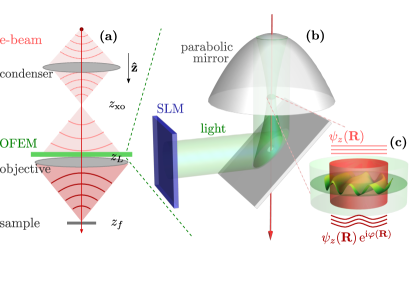
In this Letter, we propose an optical free-space electron modulator (OFEM) in which a phase profile is imprinted on the transverse electron wave function by means of stimulated elastic Compton scattering associated with the term in the light-electron coupling Hamiltonian. The absence of material structures prevents electron decoherence and enables the use of high light intensities, as required to activate ponderomotive forces. We present a simple, yet rigorous semiclassical theory that supports applications in aberration correction and transverse e-beam shaping. While optical e-beam phase stamping has been demonstrated using a continuous-wave laser in a tour-de-force experiment Schwartz et al. (2019), we envision pulsed illumination as a more feasible route to implement an OFEM, exploiting recent advances in ultrafast electron microscopy, particularly in systems that incorporate light injection with high numerical aperture Das et al. (2019) for diffraction-limited patterning of the optical field.
II Free-space optical phase imprinting
We study the free-space interaction between an e-beam and a light field represented by its vector potential . Taking the e-beam propagation direction along , it is convenient to write the electron wave function as , where denotes transverse coordinates and we separate the slowly-varying envelope from the fast oscillations imposed by the central wave vector and energy . Under typical conditions met in electron microscopes, and assuming that interaction with light only produces small variations in the electron energy compared with , we can adopt the nonrecoil approximation to reduce the Dirac equation in the minimal coupling scheme to an effective Schrödinger equation Val ,
where
is the interaction Hamiltonian, is the electron velocity, and introduces relativistic corrections to the term. This equation admits the analytical solution
where is the incident electron wave function.
We consider that the light field acts on the electron over a sufficiently short path length as to neglect any transverse variation in its wave function during interaction. We also note that the term in does not contribute to the final electron state because it represents real photon absorption or emission events, which are kinematically forbidden. Likewise, following a similar argument, under monochromatic illumination with light of frequency , the time-varying components in (), which describe two-photon emission or absorption, also produce vanishing contributions. The remaining terms represent stimulated elastic Compton scattering, a second-order process that combines virtual absorption and emission of photons, amplified by the large population of their initial and final states. An alternative description of this effect is provided by the ponderomotive force acting on a classical point-charge electron and giving rise to diffraction in the resulting effective potential Batelaan (2007). As we are interested in imprinting a phase on the electron wave function without altering its energy, we consider spectrally narrow external illumination that can be effectively regarded as monochromatic, such as that produced by laser pulses of much longer duration than the electron pulse. Writing the external field as , the transmitted wave function becomes
where
| (1) |
is an imprinted phase that depends on transverse coordinates , we define the scaled mass , and is the fine structure constant.
III Description of an OFEM
We envision an OFEM placed right before the objective lens of an electron microscope [Fig. 1(a)], in a region where the e-beam spans a large diameter ( times the light wavelength). The OFEM could consist of a combination of planar and parabolic mirrors with drilled holes that allow the e-beam to pass through the optical focal region [Fig. 1(b)]. The electron is then exposed to intense fields that can be shaped with diffraction-limited lateral resolution through a spatial light modulator and a high numerical aperture of the parabolic mirror. This results in a controlled position-dependent phase, as prescribed by Eq. (1) [Fig. 1(c)]. Considering a monochromatic e-beam and omitting for simplicity an overall time-dependent factor, free propagation of the electron wave function between planes and is described by
| (2) |
where the second line is obtained by performing the integral in the paraxial approximation (i.e., ) and we are interested in exploring positions near an electron focal point. In a simplified microscope model, we take at the entrance of the objective lens where the OFEM is also placed, and the incident electron is a spherical wave emanating from the crossover point following the condenser lens. Introducing in Eq. (2) the phase produced by an objective lens with focal distance and aperture radius , we have (see Appendix A)
| (3) |
where , we define , the phases and are produced by aberrations and the OFEM [Eq. (1)], respectively, and the integral is restricted to . In what follows, we study the electron wave function profile as given by Eq. (3) at the focal plane , defined by the condition .
Required light intensity.—From Eq. (1), the imprinted phase shift scales with the light intensity roughly as , where is the effective length of light-electron interaction, which depends on the focusing conditions of the external illumination. For example, for an electron moving along the axis of an optical paraxial vortex beam of azimuthal angular momentum number and wavelength , we have , where is the light beam divergence half-angle (see Appendix C). Under these conditions, a phase is achieved with a light power kW for 60 keV electrons and nm; this result is independent of , emphasizing the important role of phase accumulation along a long interaction region in a loosely focused light beam. This power level can be reached using nanosecond laser pulses synchronized with the electron passage through the optical field Das et al. (2019). We note that the phase scaling [see Eq. (1)] leaves some room for improvement by placing the OFEM in low-energy regions of the e-beam to reduce the optical power demand.
IV Aberration correction
As an application of lateral phase moulding, we explore the conditions needed to compensate spherical aberration, corresponding to Allen et al. (2001); Paganin et al. (2018) in Eq. (3), where is a length coefficient. Upon examination of the phase profile imprinted by paraxial light vortex beams (see Appendix B), we find that an azimuthal number produces the required radial dependence under the condition . For a typical microscope parameters mm, 60 keV electrons, m, and nm, the above condition is satisfied with . Then, compensation of spherical aberration (i.e., ) is realized with a beam power W, which is attainable using femtosecond laser pulses in ultrafast electron microscopes Feist et al. (2015); Vanacore et al. (2018); Kfir et al. (2020); Wang et al. (2020).
V Transverse e-beam shaping
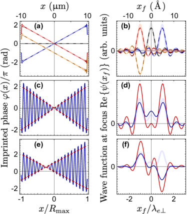
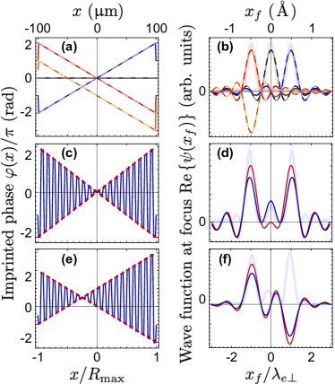
The production of on-demand electron spot profiles involves a two-step process comprising the determination of the necessary phase pattern , and from here the required optical beam parameters that generate that phase. While this is a complex task in general, we can find an approximate analytical solution for one-dimensional systems, assuming translational invariance along a direction perpendicular to the electron velocity. We therefore consider an optical beam characterized by an electric field and explore the generation of focal electron shapes defined by a wave function independent of . For light propagating along the positive direction, we can write without loss of generality with and in terms of the expansion coefficients . Inserting this expression into Eq. (1), we find (see Appendix D) , where is a global phase. Given a target profile , we can then use the approximation to generate the needed light beam coefficients. A particular solution is obtained by imposing , which renders as the square root of the right-hand side in the above expression. For any solution, combining these two integral expressions and dismissing , we find
| (4) |
which yields a diffraction-limited phase profile.
(rad)
We explore this strategy in Fig. 2, where the left panels present the OFEM phase, whereas the right ones show the corresponding color-matched wave functions obtained by inserting that phase into Eq. (3) without aberrations () and with the integral over yielding a trivial overall constant factor. Broken curves in Fig. 2(a,b) and red curves in Fig. 2(c-f) stand for target profiles, whereas the rest of the curves are obtained by accounting for optical diffraction [i.e., by transforming the target phase as prescribed by Eq. (4)]. In-plane OFEM and focal coordinates and are normalized as explained in the caption, thus defining universal curves for a specific choice of the ratio between the objective aperture radius and the light wavelength, . Linear phase profiles [Fig. 2(a)], which are well reproduced by diffraction-limited illumination, give rise to peaked electron wave functions [Fig. 2(b)] centered at positions that depend on the slope of the phase , with the offset value determining the focal peak phase. The situation is more complicated when aiming to produce two electron peaks, which can be achieved with an intermitent phase profile that combines two different slopes, either without [Fig. 2(c,d)] or with [Fig. 2(e,f)] offset to generate symmetric or antisymmetric wave functions, respectively. Light diffraction reduces the contrast of the obtained focal shapes, but still tolerates well-defined intensity peaks [Fig. 2(b,d,f), light curves], which become sharper when is increased (see Fig. 4).
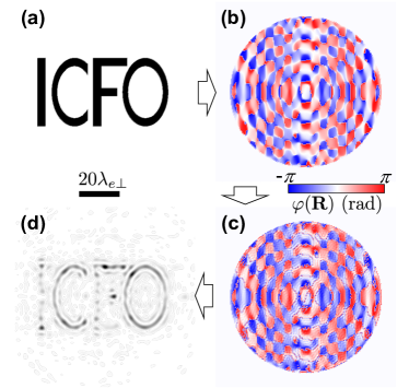
For actual two-dimensional beams, using consolidated results of image compression theory Hayes et al. (1980); Aiger and Talbot (2010), we can find approximate contour spot profiles by setting the OFEM phase to the argument of the Fourier transform of solid shapes filling those contours. This is illustrated in Fig. 3, where panel (b) represents the phase of the object in (a), while panel (c) is the actual diffraction-limited phase obtained by convoluting (b) with a point spread function (see Appendix E), which produces a blurred, but still discernible electron focal image.
VI Conclusion
In brief, shaped optical fields can modulate the electron wave function in free space to produce on-demand e-beam focal profiles. The required light intensities are reachable using pulsed illumination, currently available in ultrafast electron microscope setups. We have illustrated this idea with simple examples of target and optical profiles, but a higher degree of control over the transverse electron wave function should benefit from machine learning techniques Spurgeon et al. (2020) for the well-defined problem of finding the optimum light beam angular profile that better fits the desired e-beam spot shape. In combination with spatiotemporal light shaping, the proposed OFEM element should enable the exploration of nanoscale nonlocal correlations in sample dynamics.
Acknowledgments
We thank Mathieu Kociak and Ido Kaminer for helpful and enjoyable discussions. This work has been supported in part by ERC (Advanced Grant 789104-eNANO), the Spanish MINECO (MAT2017-88492-R and SEV2015-0522), the Catalan CERCA Program, and Fundació Privada Cellex.
Appendix A Derivation of equation (3)
We start from Eq. (2),
| (5) |
where we have inserted a transmission factor associated with a focusing lens of focal distance and aperture radius placed at the plane. Specifying the incident electron as a spherical wave emanating from the crossover point at (see Fig. 1), Eq. (5) reduces to
| (6) |
where . In Eq. (6), we dismiss an overall factor , which introduces a negligible phase modulation across the focal spot [e.g., for 60 keV electrons (nm) and mm, a change in by 1 nm produces a phase shift mrad]. This expression directly becomes Eq. (2) by defining the 2D angular coordinate and inserting in the integrand two phase correction factors due to aberrations and the OFEM, represented through and , respectively.
Appendix B Phase imprinted by paraxial optical vortex beams
The electric field associated with an external light beam propagating along positive directions admits the general expression
| (7) |
where we sum over polarizations s, p and integrate over wave vectors within the light cone , is the light wave vector component along , and are unit polarization vectors, and are expansion coefficients. We now consider beams with a well-defined azimuthal angular momentum number by setting . Inserting these coefficients in Eq. (7) and carrying out the integral, we find
| (8) |
where
are Bessel beams. We now evaluate Eq. (1) using the field of Eq. (8), which leads to
| (10) | ||||
For optical paraxial beams constructed from a limited range of transverse wave vectors , where is the divergence half-angle, with taken to be constant within that range, we use the approximation for to write the lowest-order contribution to Eq. (10) as
This approximation is valid for small arguments of the Bessel functions, that is, . For a light wavelength nm and a typical objective lens radius m, this imposes an upper limit on the divergence angle of the optical beam .
The power carried by the light beam can be obtained by integrating the Poynting vector associated with the field of Eq. (7). We find
| (11) |
where the rightmost approximation corresponds to the paraxial beam considered above. When the external light is made of only p or s polarization components, we can use Eq. (11) to recast the phase as
| (12) |
which is obviously proportional to the beam power . Interestingly, by setting we have , which has the same radial scaling as the phase associated with spherical aberration in the electron beam.
Appendix C Effective length of interaction for an paraxial light beam
For , Eq. (12) is independent of and within the paraxial approximation. This allows us to estimate the power needed to obtain a phase shift of in the electron as . Now, from Eq. (1), we can roughly estimate the phase shift as
| (13) |
where the focal field intensity is absorbed in the light intensity and is an effective light-electron interaction length that depends on the light focusing conditions. In particular, we can find for the paraxial beams considered above by first calculating the field intensity from Eq. (8) for and ; we find , which permits writing the beam power in Eq. (11) (for either s or p polarization) as , and from here and Eq. (12), we have . Comparing this expression with Eq. (13), we obtain .
Appendix D Derivation of equation (4)
The electric field of a light beam propagating along positive directions and having translational invariance along can be regarded as a combination of plane waves of wave vectors . More precisely, we can write
| (14) |
in terms of expansion coefficients . Inserting this expression into Eq. (1) and performing the integral, we find
| (15) |
Now, the function, which contributes only at , can be recast as
| (16) |
thus permitting us to carry out the integral to find
| (17) |
where is an overall phase that we dismiss because it is independent of and does not affect the electron intensity profile. Given a target OFEM phase , although the range of integration is not infinite, we can approximate the light beam coefficients as the inverse Fourier transform
| (18) |
A specific solution of this equation can be found by setting , which renders as the square root of the right-hand side of Eq. (18). For any solution, by inserting Eq. (18) into Eq. (17), we find
which is Eq. (4). The actual phase that can be imprinted with a light beam in the OFEM element [i.e., taking into account the finite range of wave vectors contributing to Eq. (14)] is the target phase convoluted with the 1D point spread function .
Appendix E Synthesis of 2D phase profiles
In the analysis of Fig. 3, we start with a black-and-white target intensity profile [e.g., and 0 in the black and white areas of Fig. 3(a)] and perform the fast Fourier transform (FFT) Press et al. (1992) to compute , where [see definitions of different variables in Eq. (3)]. We then retain only the phase of , which is known to capture the contour of the designated intensity profile Hayes et al. (1980); Aiger and Talbot (2010), so we regard it as the target phase to be delivered by the OFEM [Fig. 3(b)]. By analogy to the 1D profile analysis in Sec. D, we introduce the effects of light diffraction in a phenomenological way by first Fourier transforming , where is the light wave vector component parallel to the OFEM plane and the integral extends over the objective lens aperture defined by ; in a second step, we transform back to , only retaining diffraction-limited components [Fig. 3(c)]; this procedure is equivalent to calculating as the convolution of with the 2D point spread function . We finally obtain the actual spot profile [Fig. 3(d)] by evaluating Eq. (3) without aberrations () at the focal plane ().
Incidentally, apart from an overall normalization factor, we find that the light wavelength , the electron wave vector (or equivalently, the electron energy ), and the in-plane focal and OFEM coordinates and enter the analysis presented in this work only through the combinations [e.g., see Eq. (3)] and , where is the in-plane projection of the unit vector indicating the incident light direction, whereas is the projected focal-plane electron wavelength defined as the ratio between the de Broglie wavelength and the numerical aperture of the objective lens . By normalizing and to and , respectively, we obtain universal curves that only depend on the ratio between the aperture radius of the objective lens and the light wavelength. We use this normalization in Figs. 2 and 3, as well as in the additional Fig. 4.
Appendix F Evaluation of the OFEM phase from the incident light field amplitude
For completeness, we present a generalization of Eqs. (14) and (15) to 2D beams, for which the incident field can be expressed in general as indicated in Eq. (7). Inserting the latter into Eq. (1), performing the integral over , and using a relation similar to Eq. (16), the phase reduces to
| (19) |
where and are the azimuthal angles of and , respectively, and we define
and . Equation (19) involves a 3D integral that needs to be evaluated over the coordinates of the 2D lens aperture, thus demanding an unaffordable numerical effort consisting of operations for points per dimension. A more practical way of evaluating this expression can be found by first computing its Fourier transform
where is the azimuthal angle of . Here, the function imposes and introduces a denominator given by the derivative of its argument. After some simple algebra, we find
where . Together with the inverse Fourier transform , the evaluation now takes an affordable number of operations (i.e., a factor of for the 1D integral over and the remaining factors needed for the 2D FFTs), which can be beneficial for carrying out extensive phase calculations, as needed to train machine learning algorithms for fast determination of the light coefficients in Eq. (7).
References
- Haider et al. (1998) M. Haider, H. Rose, S. Uhlemann, E. Schwan, B. Kabius, and K. Urban, Ultramicroscopy 75, 53 (1998).
- Batson et al. (2002) P. E. Batson, N. Dellby, and O. L. Krivanek, Nature 418, 617 (2002).
- Hawkes and Spence (2019) P. Hawkes and J. Spence, Springer Handbook of Microscopy (Springer Nature Switzerland AG, 2019).
- Nellist et al. (2004) P. D. Nellist, M. F. Chisholm, N. Dellby, O. L. Krivanek, M. F. Murfitt, Z. S. Szilagyi, A. R. Lupini, A. Borisevich, W. H. Sides Jr., and S. J. Pennycook, Science 305, 1741 (2004).
- Muller et al. (2008) D. A. Muller, L. Fitting Kourkoutis, M. Murfitt, J. H. Song, H. Y. Hwang, J. Silcox, N. Dellby, and O. L. Krivanek, Science 319, 1073 (2008).
- Krivanek et al. (2014) O. L. Krivanek, T. C. Lovejoy, N. Dellby, T. Aoki, R. W. Carpenter, P. Rez, E. Soignard, J. Zhu, P. E. Batson, M. J. Lagos, et al., Nature 514, 209 (2014).
- Lagos et al. (2017) M. J. Lagos, A. Trügler, U. Hohenester, and P. E. Batson, Nature 543, 529 (2017).
- Hage et al. (2018) F. S. Hage, R. J. Nicholls, J. R. Yates, D. G. McCulloch, T. C. Lovejoy, N. Dellby, O. L. Krivanek, K. Refson, and Q. M. Ramasse, Sci. Adv. 4, eaar7495 (2018).
- Hage et al. (2019) F. S. Hage, D. M. Kepaptsoglou, Q. M. Ramasse, and L. J. Allen, Phys. Rev. Lett. 122, 016103 (2019).
- Hachtel et al. (2019) J. A. Hachtel, J. Huang, I. Popovs, S. Jansone-Popova, J. K. Keum, J. Jakowski, T. C. Lovejoy, N. Dellby, O. L. Krivanek, and J. C. Idrobo, Science 363, 525 (2019).
- Möllenstedt and Düker (1956) G. Möllenstedt and H. Düker, Zeitschrift für Physik 145, 377 (1956).
- Guzzinati et al. (2017) G. Guzzinati, A. Beche, H. Lourenco-Martins, J. Martin, M. Kociak, and J. Verbeeck, Nat. Commun. 8, 14999 (2017).
- Béché et al. (2014) A. Béché, R. Van Boxem, G. Van Tendeloo, and J. Verbeeck, Nat. Phys. 10, 26 (2014).
- Verbeeck et al. (2018) J. Verbeeck, A. Béché, K. Müller-Caspary, G. Guzzinati, M. A. Luong, and M. D. Hertog, Ultramicroscopy 190, 58 (2018).
- Verbeeck et al. (2010) J. Verbeeck, H. Tian, and P. Schattschneider, Nature 467, 301 (2010).
- McMorran et al. (2011) B. J. McMorran, A. Agrawal, I. M. Anderson, A. A. Herzing, H. J. Lezec, J. J. McClelland, and J. Unguris, Science 331, 192 (2011).
- Shiloh et al. (2014) R. Shiloh, Y. Lereah, Y. Lilach, and A. Arie, Ultramicroscopy 144, 26 (2014).
- Grillo et al. (2017) V. Grillo, A. H. Tavabi, E. Yucelen, P.-H. Lu, F. Venturi, H. Larocque, L. Jin, A. Savenko, G. C. Gazzadi, R. Balboni, et al., Opt. Express 25, 21851 (2017).
- Shiloh et al. (2018) R. Shiloh, R. Remez, P.-H. Lu, L. Jin, Y. Lereah, A. H. Tavabi, R. E. Dunin-Borkowski, and A. Arie, Ultramicroscopy 189, 46 (2018).
- Kapitza and Dirac (1933) P. L. Kapitza and P. A. M. Dirac, Proc. Cambridge Philos. Soc. 29, 297 (1933).
- Freimund et al. (2001) D. L. Freimund, K. Aflatooni, and H. Batelaan, Nature 413, 142 (2001).
- Freimund and Batelaan (2002) D. L. Freimund and H. Batelaan, Phys. Rev. Lett. 89, 283602 (2002).
- Batelaan (2007) H. Batelaan, Rev. Mod. Phys. 79, 929 (2007).
- García de Abajo (2010) F. J. García de Abajo, Rev. Mod. Phys. 82, 209 (2010).
- Koz’ak et al. (2018) M. Koz’ak, N. Schönenberger, and P. Hommelhoff, Phys. Rev. Lett. 120, 103203 (2018).
- Koz’ak (2019) M. Koz’ak, Phys. Rev. Lett. 123, 203202 (2019).
- Black et al. (2019) D. S. Black, U. Niedermayer, Y. Miao, Z. Zhao, O. Solgaard, R. L. Byer, and K. J. Leedle, Phys. Rev. Lett. 123, 264802 (2019).
- Schn̈enberger et al. (2019) N. Schn̈enberger, A. Mittelbach, P. Yousefi, J. McNeur, U. Niedermayer, and P. Hommelhoff, Phys. Rev. Lett. 123, 264803 (2019).
- Howie (1999) A. Howie, Inst. Phys. Conf. Ser. 161, 311 (1999).
- García de Abajo and Kociak (2008) F. J. García de Abajo and M. Kociak, New J. Phys. 10, 073035 (2008).
- Howie (2009) A. Howie, Microsc. Microanal. 15, 314 (2009).
- Pomarico et al. (2018) E. Pomarico, I. Madan, G. Berruto, G. M. Vanacore, K. Wang, I. Kaminer, F. J. García de Abajo, and F. Carbone, ACS Photonics 5, 759 (2018).
- Barwick et al. (2009) B. Barwick, D. J. Flannigan, and A. H. Zewail, Nature 462, 902 (2009).
- García de Abajo et al. (2010) F. J. García de Abajo, A. Asenjo Garcia, and M. Kociak, Nano Lett. 10, 1859 (2010).
- Park et al. (2010) S. T. Park, M. Lin, and A. H. Zewail, New J. Phys. 12, 123028 (2010).
- Park and Zewail (2012) S. T. Park and A. H. Zewail, J. Phys. Chem. A 116, 11128 (2012).
- Kirchner et al. (2014) F. O. Kirchner, A. Gliserin, F. Krausz, and P. Baum, Nat. Photon. 8, 52 (2014).
- Piazza et al. (2015) L. Piazza, T. T. A. Lummen, E. Quiñonez, Y. Murooka, B. Reed, B. Barwick, and F. Carbone, Nat. Commun. 6, 6407 (2015).
- Feist et al. (2015) A. Feist, K. E. Echternkamp, J. Schauss, S. V. Yalunin, S. Schäfer, and C. Ropers, Nature 521, 200 (2015).
- Lummen et al. (2016) T. T. A. Lummen, R. J. Lamb, G. Berruto, T. LaGrange, L. D. Negro, F. J. García de Abajo, D. McGrouther, B. Barwick, and F. Carbone, Nat. Commun. 7, 13156 (2016).
- Echternkamp et al. (2016) K. E. Echternkamp, A. Feist, S. Schäfer, and C. Ropers, Nat. Phys. 12, 1000 (2016).
- Ryabov and Baum (2016) A. Ryabov and P. Baum, Science 353, 374 (2016).
- Vanacore et al. (2016) G. M. Vanacore, A. W. P. Fitzpatrick, and A. H. Zewail, Nano Today 11, 228 (2016).
- Kozák et al. (2017) M. Kozák, J. McNeur, K. J. Leedle, H. Deng, N. Schönenberger, A. Ruehl, I. Hartl, J. S. Harris, R. L. Byer, and P. Hommelhoff, Nat. Commun. 8, 14342 (2017).
- Feist et al. (2017) A. Feist, N. Bach, T. D. N. Rubiano da Silva, M. Mäller, K. E. Priebe, T. Domräse, J. G. Gatzmann, S. Rost, J. Schauss, S. Strauch, et al., Ultramicroscopy 176, 63 (2017).
- Priebe et al. (2017) K. E. Priebe, C. Rathje, S. V. Yalunin, T. Hohage, A. Feist, S. Schäfer, and C. Ropers, Nat. Photon. 11, 793 (2017).
- Vanacore et al. (2018) G. M. Vanacore, I. Madan, G. Berruto, K. Wang, E. Pomarico, R. J. Lamb, D. McGrouther, I. Kaminer, B. Barwick, F. J. García de Abajo, et al., Nat. Commun. 9, 2694 (2018).
- Morimoto and Baum (2018a) Y. Morimoto and P. Baum, Phys. Rev. A 97, 033815 (2018a).
- Morimoto and Baum (2018b) Y. Morimoto and P. Baum, Nat. Phys. 14, 252 (2018b).
- Das et al. (2019) P. Das, J. D. Blazit, M. Tencé, L. F. Zagonel, Y. Auad, Y. H. Lee, X. Y. Ling, A. Losquin, O. S. C. Colliex, F. J. García de Abajo, et al., Ultramicroscopy 203, 44 (2019).
- Vanacore et al. (2019) G. M. Vanacore, G. Berruto, I. Madan, E. Pomarico, P. Biagioni, R. J. Lamb, D. McGrouther, O. Reinhardt, I. Kaminer, B. Barwick, et al., Nat. Mater. 18, 573 (2019).
- Kfir (2019) O. Kfir, Phys. Rev. Lett. 123, 103602 (2019).
- Di Giulio et al. (2019) V. Di Giulio, M. Kociak, and F. J. García de Abajo, Optica 6, 1524 (2019).
- Talebi (2020) N. Talebi, Phys. Rev. Lett. 125, 080401 (2020).
- Kfir et al. (2020) O. Kfir, H. Lourenço-Martins, G. Storeck, M. Sivis, T. R. Harvey, T. J. Kippenberg, A. Feist, and C. Ropers, Nature 582, 46 (2020).
- Wang et al. (2020) K. Wang, R. Dahan, M. Shentcis, Y. Kauffmann, A. B. Hayun, O. Reinhardt, S. Tsesses, and I. Kaminer, Nature 582, 50 (2020).
- García de Abajo et al. (2016) F. J. García de Abajo, B. Barwick, and F. Carbone, Phys. Rev. B 94, 041404(R) (2016).
- Cai et al. (2018) W. Cai, O. Reinhardt, I. Kaminer, and F. J. García de Abajo, Phys. Rev. B 98, 045424 (2018).
- Konečná and García de Abajo (2020) A. Konečná and F. J. García de Abajo, Phys. Rev. Lett. 125, 030801 (2020).
- Schwartz et al. (2019) O. Schwartz, J. J. Axelrod, S. L. Campbell, C. Turnbaugh, R. M. Glaeser, and H. Müller, Nat. Methods 16, 1016 (2019).
- (61) A. Valerio and F. J. García de Abajo, in preparation.
- Allen et al. (2001) L. J. Allen, M. P. Oxley, and D. Paganin, Phys. Rev. Lett. 87, 123902 (2001).
- Paganin et al. (2018) D. M. Paganin, T. C. Petersen, and M. A. Beltran, Phys. Rev. A 97, 023835 (2018).
- Hayes et al. (1980) M. Hayes, Jae Lim, and A. Oppenheim, IEEE Transactions on Acoustics, Speech, and Signal Processing 28, 672 (1980).
- Aiger and Talbot (2010) D. Aiger and H. Talbot, in 2010 IEEE Computer Society Conference on Computer Vision and Pattern Recognition (2010), pp. 295–302.
- Spurgeon et al. (2020) S. R. Spurgeon, C. Ophus, L. Jones, A. Petford-Long, S. V. Kalinin, M. J. Olszta, R. E. Dunin-Borkowski, N. Salmon, K. Hattar, W.-C. D. Yang, et al., Nat. Mater. pp. DOI: 10.1038/s41563–020–00833–z (2020).
- Press et al. (1992) W. H. Press, S. A. Teukolsky, W. T. Vetterling, and B. P. Flannery, Numerical Recipes (Cambridge University Press, New York, 1992).