Acoustic spin Hall effect in strong spin-orbit metals
We report on the observation of the acoustic spin Hall effect that facilitates lattice motion induced spin current via spin orbit interaction (SOI). Under excitation of surface acoustic wave (SAW), we find a spin current flows orthogonal to the propagation direction of a surface acoustic wave (SAW) in non-magnetic metals. The acoustic spin Hall effect manifests itself in a field-dependent acoustic voltage in non-magnetic metal (NM)/ferromagnetic metal (FM) bilayers. The acoustic voltage takes a maximum when the NM layer thickness is close to its spin diffusion length, vanishes for NM layers with weak SOI and increases linearly with the SAW frequency. To account for these results, we find the spin current must scale with the SOI and the time derivative of the lattice displacement. Such form of spin current can be derived from a Berry electric field associated with time varying Berry curvature and/or an unconventional spin-lattice interaction mediated by SOI. These results, which imply the strong coupling of electron spins with rotating lattices via the SOI, show the potential of lattice dynamics to supply spin current in strong spin orbit metals.
Spin current represents a flow of spin angular momentum carried by electrons. The spin Hall effectDyakonov and Perel (1971) allows electrical generation of spin current in materials with strong spin orbit interaction (SOI)Galitski and Spielman (2013). The spin Hall angle, a material parameter that characterizes charge to spin conversion efficiency, scales with the longitudinal resistivity and the spin Hall conductivityHoffmann (2013). For the intrinsic spin Hall effect, the spin Hall conductivity is determined by the electron band structureSinova et al. (2004); Guo et al. (2008) (i.e., the Berry curvature of the bands near the Fermi level) and the SOI of the host material. As spin current can be used to control the direction of magnetization of a ferromagnetic layer placed adjacent to the spin source, developing materials and means to create it with high efficiency are the forefront of modern SpintronicsMiron et al. (2011); Liu et al. (2012); Manchon et al. (2019).
Recent studies have shown that not only electrons but other degrees of freedom can generate spin current. Precessing magnetization pumps out spin current from magnetic materials, a mechanism known as spin pumpingMizukami et al. (2002); Tserkovnyak et al. (2002); Saitoh et al. (2006). In the spin Seebeck effectUchida et al. (2010); Bauer et al. (2012), a temperature gradient applied to a magnetic material induces a magnon population gradient and the associated diffusion spin current. Spin current can also be produced from exchange of angular momentum between a rotating body and electrons, an effect referred to as spin-rotation couplingMatsuo et al. (2013). The effect has been observed in liquid metalsTakahashi et al. (2016) and non-magnetic light metals (e.g., Cu)Kobayashi et al. (2017). Generation of spin current via spin pumping, spin Seebeck effect and spin-rotation coupling do not require large SOI of the host material.
Here we show a profoundly different approach to generate spin current. We find a spin current directly emerges from the dynamics of lattice via SOI. Similar to the spin Hall effect where a spin current flows transverse to electrical current, a spin current develops orthogonal to the propagation direction of a surface acoustic wave (SAW) in non-magnetic metals. The efficiency to generate spin current is proportional to the spin Hall angle and may be influenced by a factor that depends on the film structure. To account for the experimental results, we find the spin current must scale with the SOI and the time derivative of the lattice displacement.
Thin film heterostructures are grown on piezoelectric LiNbO3 substrates using radio frequency (rf) magnetron sputtering. The film structure is sub./X()/CoFeB(1)/MgO(2)/Ta(1) with X=W, Pt, Ta and Cu (thickness in unit of nanometers). The heterostructures are referred to as X/CoFeB bilayers hereafter. Standard optical lithography is used to pattern Hall bars from the film and electrodes/interdigital transducers (IDTs)White and Voltmer (1965) from conducting metals (see Methods for the details of sample preparation).
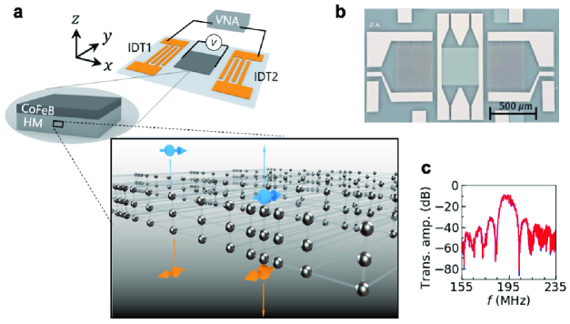
The experimental setup and the coordinate system are schematically illustrated in Fig. 1(a). The Hall bar is placed between the two IDTs. Figure 1(b) shows a representative optical microscope image of the device. A vector network analyzer (VNA) is connected to the IDTs to excite a Rayleigh-type SAW from one end and to detect its transmission at the other end. Figure 1(c) shows typical transmission spectra with a W/CoFeB bilayer placed between the IDTs. The transmission amplitude takes a maximum at 194 MHz, which corresponds to the fundamental excitation frequency of the SAW () defined by the geometry of the IDTs and the sound velocity of the substrate.
The acoustoelectric properties of the films are studied as a function of magnetic field. A continuous rf signal with fixed frequency and power is fed from one of the VNA ports to the corresponding IDT, which launches a SAW along that propagates to the film and induces lattice motion. The longitudinal (along ) and transverse (along ) voltages of the Hall bar, defined as and , respectively, are measured during the SAW excitation. Since and contain similar information, here we focus on the results of ; see supplementary material section LABEL:sec:supp:results for the characteristics of . In order to extract the voltage originating from the SAW, we subtract the average voltage measured under off-resonance conditions () and obtain the acoustic voltage . is the average value of when is set far from (see Methods for the details). We apply an in-plane magnetic field of magnitude during the voltage measurements. The angle between the field and the -axis is defined as . As the magnetic easy axis of the CoFeB layer points along the film plane and the in-plane magnetic anisotropy is weak, we assume the orientation of the magnetization follows that of the magnetic field.
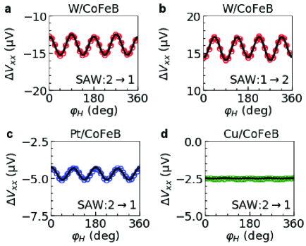
Figures 2(a,c,d) show the field angle () dependence of for W/CoFeB, Pt/CoFeB and Cu/CoFeB bilayers when a rf signal of and 10 dBm is applied to IDT2. For W/CoFeB and Pt/CoFeB bilayers, shows a sinusoidal variation with a period of 90∘. Note that the sign (i.e., the phase) of the sinusoidal variation is the same for the two bilayers although the sign of the spin Hall angle is opposite between Pt and WHoffmann (2013). In contrast, no such variation is found for the Cu/CoFeB bilayer. Figure 2(b) shows vs. of the W/CoFeB bilayer when the rf signal is applied to IDT1. Clearly, the mean offset voltage and the sinusoidal variation change their signs as the SAW propagation direction is reversed. Similar features are observed for the Pt/CoFeB bilayers.
We fit the dependence of with the following function:
| (1) |
where (2,4) represents the coefficient of the sinusoidal function with a period of and is the -independent component. is proportional to what is known as the acoustic current, which originates from rectification of the localized electric field and charge densityWeinreich and White (1957).
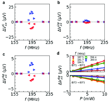
The dependence of is plotted in Fig. 3(a). takes a peak at 194 MHz, which corresponds to (see Fig. 1(c)), and changes its sign as the SAW propagation direction is reversedKawada et al. (2019). The dependence of and are shown in Figs. 3(b) and 3(c), respectively. is significantly larger than and shows a clear peak at , suggesting that its appearance is associated with the excitation of SAW. The rf power () dependence of is shown in Fig. 3(d). increases linearly with .
To identify the origin of , we have studied its dependence on the X layer thickness (). Hereafter, we use and to represent the corresponding value at . As the transmittance of the SAW slightly varies from device to device due to subtle differences in the IDTs, we normalize with and define . Figure 4(a) shows the -dependence of for W/CoFeB bilayers. We find takes a maximum at nm. Interestingly, such -dependence of resembles that of the spin Hall magnetoresistance (SMR)Nakayama et al. (2013); Chen et al. (2013). The -dependence of the SMR ratio, is plotted in Fig. 4(b). represents the resistance change when the magnetization of the CoFeB layer is rotated in the planeKim et al. (2016) and is the base resistance that does not vary with . Clearly, the -dependence of and are similar. According to the drift-diffusion model of spin transport in non-magnetic metal (NM)/ferromagnetic metal (FM) bilayersChen et al. (2013); Kim et al. (2016), the maximum of is proportional to the square of the NM layer spin Hall angle (), and the NM layer thickness at the maximum is close to its spin diffusion length (). Using the model (see Methods), we obtain and nm from the -dependence of for W, which are in good agreement with previous studiesKim et al. (2016).
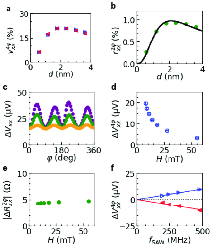
The similarity in the -dependence of and suggests that a spin current is generated in the X layer. The fact that is almost absent for Cu/CoFeB bilayers (see Fig. 2(d)) further supports this notion: the spin Hall angle of Cu is significantly smaller than that of Pt and W. Note, however, that there are a few differences between the acoustic voltage and the SMR. First, the field-angle dependence of the two is different. Typically the resistance due to SMR varies as (see for example, Ref. Nakayama et al. (2013)), whereas the dominant contribution to the acoustic voltage varies as . Second, is more than one order of magnitude larger than . Third, we find a striking difference in the magnetic field magnitude () dependence between the two. In Fig. 4(c), we show the dependence of vs. for W/CoFeB bilayer. As evident, the offset voltage () hardly changes with . In contrast, the magnitude of increases with decreasing . The dependence of , plotted in Figs. 4(d), shows that scales with . As a reference, we show in Fig. 4(e) the dependence of . Contrary to , is nearly constant against .
To account for these results, we modify the drift-diffusion model of spin transport that is used to describe SMRChen et al. (2013). First, we include SAW-induced straining of the FM layer and magnetoelastic couplingGowtham et al. (2016); Lau et al. (2017), which cause changes in the magnetization direction with respect to the magnetic fieldWeiler et al. (2011); Dreher et al. (2012). Consequently, acquires an extra factor of compared to the resistance change that originates from SMR. (See supplementary material section LABEL:sec:supp:results where we show that is absent for W/NiFe bilayer due to the small magnetoelastic coupling of NiFe.) Next, to generate a (rectified) dc current, the spin current must vary in time and space such that it couples to the motion of magnetic moments driven by the SAW-induced strain. We find the following form of spin current (electron spin orientation along and flow along ) produces a rectified dc current and accounts for the experimental results:
| (2) |
where is the lattice displacement along the wave propagation direction (). is a prefactor that determines the spin current generation efficiency and is proportional to , the SOI.
The spin current generated in the NM layer drifts to the NM/FM interface and causes spin accumulation. The accumulated spin at the interface causes a back flow of spin current within the NM layer, which is converted to electrical current via the inverse spin Hall effectSaitoh et al. (2006). The amount of spin accumulation at the interface depends on the direction of the FM layer magnetization due to the action of spin transfer torqueNakayama et al. (2013); Chen et al. (2013), thus causing the dependent acoustic voltage. The resulting acoustic voltage reads (see supplementary material section LABEL:sec:supp:model)
| (3) |
where is a constant that depends on the material and the geometry of the device, characterizes the -dependence similar to that of the SMR (see Eq. (4)), is the wave vector of the Rayleigh-type SAW (sgn takes the sign of ), and and are, respectively, the magnetoelastic coupling constant and the saturation magnetization of the FM layer.
Equation (3) captures many features of the acoustic voltage found in the experiments. As evident, varies as . The coefficient of in Eq. (3), equivalent to , changes its sign upon reversal of the wave propagation direction (defined by the sign of ), scales with and , and is proportional to the square of the spin orbit coupling of the NM layer, and thus independent of the sign of the NM layer spin Hall angle. The thickness dependence of , coded in , is in relatively good agreement with the experimental results. We have also studied the dependence of for W/CoFeB bilayer; the results are plotted in Fig. 4(f). As evident, scales with . We emphasize that Eq. (2) is the only form of spin current that can account for these results. Note that the linear dependence of with excludes contributions from spin-dependent inertial forceMatsuo et al. (2017) and related effects in the presence of SOIFunato and Kohno (2018), which are proportional to higher order of .
These results therefore demonstrate that the lattice motion induces a spin current. Recent studies have shown that spin-rotation couplingMatsuo et al. (2013); Takahashi et al. (2016) can induce spin accumulation in the NM layer, which results in generation of spin current if the NM layer thickness is larger than the SAW decay length (typically, of the order the SAW wavelength, which is a few m here)Kobayashi et al. (2017). To clarify the role of spin-rotation coupling, we have studied of inverted structures, CoFeB/W bilayers. In both W/CoFeB and CoFeB/W bilayers, spin-rotation coupling induces spin density in the W layer, which can cause a flow of spin current toward the CoFeB layer as the latter can act as a spin sink. If such spin current were to flow, the flow direction will be opposite for the normal (W/CoFeB) and inverted (CoFeB/W) structures and consequently results in with opposite sign. We find that the signs of for W/CoFeB and CoFeB/W bilayers are the same, demonstrating that spin-rotation coupling is not the source of spin current (see supplementary material sections LABEL:sec:supp:results and LABEL:sec:supp:artifact). For the same reason, we can rule out SAW-induced spin pumpingWeiler et al. (2011); Uchida et al. (2011) from the CoFeB layer and the inverse spin Hall effect of the W layer. This is also supported by the fact that the signs of for W/CoFeB and Pt/CoFeB bilayers are the same (see Fig. 2) albeit the difference in the sign of for W and Pt.
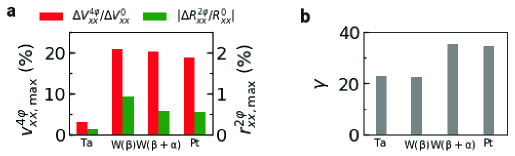
In Fig. 5(a), we summarize the maximum value of and when is varied, denoted as and , respectively, for each bilayer (X=Ta, W, Pt). Results from the CoFeB/W bilayers are included. Note that the structure of W depends on the growth condition: from the film resistivityPetroff et al. (1973); Pai et al. (2012), we consider W forms a highly-resistive -phase in W/CoFeB bilayer whereas it is a mixture of the -phase and the low-resistivity crystalline -phase in CoFeB/W bilayer. Consequently, the SMR ratio () is smaller for the latter due to the smaller Pai et al. (2012); Liu et al. (2015); Sui et al. (2017). Interestingly, we find that takes nearly the same value for the two bilayers, indicating that there are factors other than that sets the magnitude of . In Fig. 5(b), we plot the ratio to characterize such contribution. We find is significantly larger for bilayers with Pt and (+)-W (CoFeB/W) than that with -W (W/CoFeB) and Ta. Since the former two layers are textured whereas the latter two are highly disordered (i.e., amorphous-like), we consider the texture of the films may influence . Little correlation is found between and the bulk modulus of the X layer.
Finally, we discuss the source of spin current that scales with the time derivative of lattice displacement (Eq. (2)). First, a conventional mechanism would be to consider internal electric field associated with the SAW and the resulting spin Hall effect of the NM layer. There are two major sources of internal electric field. One is the piezoelectric field () localized at the film/substrate interface. Spin current generated from can only reach the NM/FM interface when the film thickness is smaller than . The thickness dependence of (Fig. 4(a)) rules out such contribution. The other source is the time varying electric field () caused by the motion of ionsPippard (1955); Holstein (1959); Blount (1959). is uniform along the film normal as long as the film thickness is significantly smaller than the SAW decay length. In general, is screened by the conduction electrons in metallic films: we infer it generates negligible spin current. With the current understanding, we consider it is difficult to quantitatively account for the experimental results with the combination of the SAW induced electric field and the spin Hall effect. Second, Eq. (2) can be derived assuming the following interactionPavlov and Firsov (1966); Romano et al. (2008): , where is a constant, is the lattice displacement vector, and and are electron momentum and spin orientation, respectively. This interaction derives from the SOIPavlov and Firsov (1966); Romano et al. (2008) and the coefficient is proportional to , similar to the relation between and . resembles the Rashba HamiltonianBychkov and Rashba (1984) but can exist here since the inversion symmetry is broken by the dynamical lattice displacement . Further studies are required, however, to justify the presence of such Hamiltonian. Third, the time derivative of the lattice displacement can cause changes in the Berry curvature of electron wave function. Indeed, theoretical studies have identified the right hand side of Eq. (2) as the Berry electric fieldSundaram and Niu (1999); Chaudhary et al. (2018). It remains to be seen whether spin current emerges from the Berry electric field under strong SOI. Finally, the phonon angular momentumZhang and Niu (2014); Garanin and Chudnovsky (2015); Holanda et al. (2018) may contribute to the generation of spin current. Similar to the spin Seebeck effectUchida et al. (2010), where the spin angular momentum of magnons are transferred to electrons, the angular momentum of phonons (i.e. sound waves) can be transferred to the electrons and induce spin current. The efficiency of such process must be addressed to assess its contribution.
In summary, we have shown that spin current is directly created from lattice motion associated with surface acoustic wave (SAW). Such acoustic spin Hall effect is observed in non-magnetic metal (NM)/ferromagnetic metal (FM) bilayers through a field-dependent dc acoustic voltage. The acoustic voltage roughly scales with the square of the spin Hall angle of the NM layer and is proportional to the SAW frequency. The NM layer thickness dependence of the acoustic voltage is similar to that of the spin Hall magnetoresistance. Using a diffusive spin transport model, we show that such characteristics of the acoustic voltage can be accounted for when a spin current that scales with the time derivative of lattice displacement is generated in the NM layer. Possible sources of such spin current include a Berry electric field associated with time varying Berry curvature and/or an unconventional SOI-mediated spin-lattice interaction that resembles the form of Rashba Hamiltonian. The efficiency to generate spin current, represented by the maximum acoustic voltage, also seems to depend on a factor related to the film texture; the efficiency is nearly the same for amorphous-like -W and textured Pt despite the difference in their spin Hall angle. The finding of the acoustic spin Hall effect thus implies a mechanism that facilitates an SOI mediated coupling of electron spins and a rotating lattice. Further studies are required to unveil the microscopic mechanism to describe such coupling.
I Materials and Methods
I.1 Sample preparation
Radio frequency magnetron sputtering is used to deposit the films on piezoelectric Y+128∘-cut LiNbO3 substrates. The film structure is sub./X()/CoFeB(1)/MgO(2)/Ta(1) with X=W, Pt, Ta and Cu (thickness in unit of nanometers). The inverted structure is sub./MgO(2)/CoFeB(1)/X()/MgO(2)/Ta(1) with X=W. The MgO(2)/Ta(1) layers serve as a capping layer to prevent oxidation of the films. For bilayers with X=Pt and Cu, a 0.5 nm thick Ta layer is inserted before deposition of X to promote their smooth growth. Hall bars are formed from the films using optical lithography and Ar ion etching. Subsequently, we use optical lithography and a liftoff process to form interdigital transducers (IDTs) and electrodes made of Ta(5)/Cu(100)/Pt(5).
Schematic illustration of the SAW device and definition of the coordinate system are shown in Fig. 6. The distance of the two IDTs is 600 m and each IDT has 20 pairs of single-type fingers. The width and gap of the fingers are set to : the corresponding SAW wavelength is . The finger overlap, i.e., the SAW aperture (), is fixed to m. A Hall bar made of the film is placed at the center of the two IDTs. The length and width of the Hall bar are set to m and m, respectively.
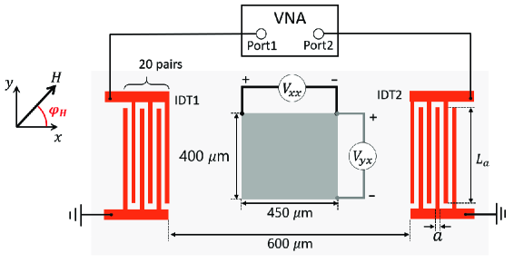
We vary to change the SAW resonance frequency (). is fixed to m for most of the results shown, which gives MHz. In Fig. 4(f), we vary to change : is set to 5, 4, 3, 2 m to obtain of 194, 242, 321, 479 MHz, respectively.
I.2 Voltage measurements
The longitudinal (along ) and transverse (along ) voltages, defined as and , respectively, are measured during the SAW excitation. To extract the voltage originating from the SAW, we subtract the average voltage measured under off-resonance conditions, defined as . is obtained as follows. Under a fixed magnetic field and rf power, we study the frequency () dependence of . takes a peak when . We choose frequencies () that are outside the peak structure of , typically a few tens of MHz away from (see Fig. 1(c) for a typical transmission spectra). is the average value of measured at several . is subtracted from the measured voltage at frequency to obtain the acoustic voltage . is always measured prior to the measurement of at frequency . Voltage measurements at each condition are repeated 5-100 times to improve the signal to noise ratio.
I.3 Spin Hall magnetoresistance
In the main text, we have used , the resistance change when the magnetization of the CoFeB layer is rotated in the plane, to estimate SMR. is equal to the sum of the SMR and the anisotropic magnetoresistance (AMR). Since the latter is significantly smaller than the former for the system under studyKim et al. (2016), we assume represents the SMR. To obtain the SMR more accurately, it is customary to measure the resistance change when the magnetization of the CoFeB layer is rotated in the planeNakayama et al. (2013), defined as . We have verified that and take similar value, justifying the assumption that represents the SMR.
The X layer thickness dependence of the spin Hall magnetoresistance is fitted using the following equationNakayama et al. (2013); Chen et al. (2013):
| (4) | ||||
where , and are the resistivity and thickness of the FM (=CoFeB) layer, respectively and is the resistivity of the X layer. Here we have assumed a transparent X/FM interface for spin transmission and neglected the effect of longitudinal spin absorption of the FM layerKim et al. (2016). The base longitudinal resistance is defined as the resistance when the magnetization of the FM layer points along the -axis. For fitting the data (Fig. 4(b)) with Eq. (4), we have used cm and cm.
Acknowledgements.
This work was partly supported by JSPS Grant-in-Aid for Specially Promoted Research (15H05702), and the Center of Spintronics Research Network of Japan.References
- Dyakonov and Perel (1971) M. I. Dyakonov and V. I. Perel, “Possibility of orienting electron spins with current,” JETP Letters 13, 467 (1971).
- Galitski and Spielman (2013) V. Galitski and I. B. Spielman, “Spin-orbit coupling in quantum gases,” Nature 494, 49 (2013).
- Hoffmann (2013) Axel Hoffmann, “Spin hall effects in metals,” IEEE Trans. Magn. 49, 5172 (2013).
- Sinova et al. (2004) J. Sinova, D. Culcer, Q. Niu, N. A. Sinitsyn, T. Jungwirth, and A. H. MacDonald, “Universal intrinsic spin hall effect,” Phys. Rev. Lett. 92, 126603 (2004).
- Guo et al. (2008) G. Y. Guo, S. Murakami, T. W. Chen, and N. Nagaosa, “Intrinsic spin hall effect in platinum: First-principles calculations,” Phys. Rev. Lett. 100, 096401 (2008).
- Miron et al. (2011) I. M. Miron, K. Garello, G. Gaudin, P. J. Zermatten, M. V. Costache, S. Auffret, S. Bandiera, B. Rodmacq, A. Schuhl, and P. Gambardella, “Perpendicular switching of a single ferromagnetic layer induced by in-plane current injection,” Nature 476, 189 (2011).
- Liu et al. (2012) Luqiao Liu, Chi-Feng Pai, Y. Li, H. W. Tseng, D. C. Ralph, and R. A. Buhrman, “Spin-torque switching with the giant spin hall effect of tantalum,” Science 336, 555 (2012).
- Manchon et al. (2019) A. Manchon, J. Zelezny, I. M. Miron, T. Jungwirth, J. Sinova, A. Thiaville, K. Garello, and P. Gambardella, “Current-induced spin-orbit torques in ferromagnetic and antiferromagnetic systems,” Rev. Mod. Phys. 91, 035004 (2019).
- Mizukami et al. (2002) S. Mizukami, Y. Ando, and T. Miyazaki, “Effect of spin diffusion on gilbert damping for a very thin permalloy layer in cu/permalloy/cu/pt films,” Phys. Rev. B 66, 104413 (2002).
- Tserkovnyak et al. (2002) Y. Tserkovnyak, A. Brataas, and G. E. W. Bauer, “Enhanced gilber damping in thin ferromagnetic films,” Phys. Rev. Lett. 88, 117601 (2002).
- Saitoh et al. (2006) E. Saitoh, M. Ueda, H. Miyajima, and G. Tatara, “Conversion of spin current into charge current at room temperature: Inverse spin-hall effect,” Appl. Phys. Lett. 88, 182509 (2006).
- Uchida et al. (2010) K. Uchida, J. Xiao, H. Adachi, J. Ohe, S. Takahashi, J. Ieda, T. Ota, Y. Kajiwara, H. Umezawa, H. Kawai, G. E. W. Bauer, S. Maekawa, and E. Saitoh, “Spin seebeck insulator,” Nat. Mater. 9, 894 (2010).
- Bauer et al. (2012) G. E. W. Bauer, E. Saitoh, and B. J. van Wees, “Spin caloritronics,” Nat. Mater. 11, 391 (2012).
- Matsuo et al. (2013) Mamoru Matsuo, Jun’ichi Ieda, Kazuya Harii, Eiji Saitoh, and Sadamichi Maekawa, “Mechanical generation of spin current by spin-rotation coupling,” Phys. Rev. B 87, 180402 (2013).
- Takahashi et al. (2016) R. Takahashi, M. Matsuo, M. Ono, K. Harii, H. Chudo, S. Okayasu, J. Ieda, S. Takahashi, S. Maekawa, and E. Saitoh, “Spin hydrodynamic generation,” Nat. Phys. 12, 52 (2016).
- Kobayashi et al. (2017) D. Kobayashi, T. Yoshikawa, M. Matsuo, R. Iguchi, S. Maekawa, E. Saitoh, and Y. Nozaki, “Spin current generation using a surface acoustic wave generated via spin-rotation coupling,” Phys. Rev. Lett. 119, 077202 (2017).
- White and Voltmer (1965) R. M. White and F. W. Voltmer, “Direct piezoelectric coupling to surface elastic waves,” Appl. Phys. Lett. 7, 314 (1965).
- Weinreich and White (1957) G. Weinreich and H. G. White, “Observation of the acoustoelectric effect,” Phys. Rev. 106, 1104 (1957).
- Kawada et al. (2019) T. Kawada, M. Kawaguchi, and M. Hayashi, “Unidirectional planar hall voltages induced by surface acoustic waves in ferromagnetic thin films,” Phys. Rev. B 99, 184435 (2019).
- Nakayama et al. (2013) H. Nakayama, M. Althammer, Y. T. Chen, K. Uchida, Y. Kajiwara, D. Kikuchi, T. Ohtani, S. Geprags, M. Opel, S. Takahashi, R. Gross, G. E. W. Bauer, S. T. B. Goennenwein, and E. Saitoh, “Spin hall magnetoresistance induced by a nonequilibrium proximity effect,” Phys. Rev. Lett. 110, 206601 (2013).
- Chen et al. (2013) Y. T. Chen, S. Takahashi, H. Nakayama, M. Althammer, S. T. B. Goennenwein, E. Saitoh, and G. E. W. Bauer, “Theory of spin hall magnetoresistance,” Phys. Rev. B 87, 144411 (2013).
- Kim et al. (2016) Junyeon Kim, Peng Sheng, Saburo Takahashi, Seiji Mitani, and Masamitsu Hayashi, “Spin hall magnetoresistance in metallic bilayers,” Phys. Rev. Lett. 116, 097201 (2016).
- Gowtham et al. (2016) P. G. Gowtham, G. M. Stiehl, D. C. Ralph, and R. A. Buhrman, “Thickness-dependent magnetoelasticity and its effects on perpendicular magnetic anisotropy in ta/cofeb/mgo thin films,” Phys. Rev. B 93, 024404 (2016).
- Lau et al. (2017) Yong-Chang Lau, Peng Sheng, Seiji Mitani, Daichi Chiba, and Masamitsu Hayashi, “Electric field modulation of the non-linear areal magnetic anisotropy energy,” Appl. Phys. Lett. 110, 022405 (2017).
- Weiler et al. (2011) M. Weiler, L. Dreher, C. Heeg, H. Huebl, R. Gross, M. S. Brandt, and S. T. B. Goennenwein, “Elastically driven ferromagnetic resonance in nickel thin films,” Phys. Rev. Lett. 106, 117601 (2011).
- Dreher et al. (2012) L. Dreher, M. Weiler, M. Pernpeintner, H. Huebl, R. Gross, M. S. Brandt, and S. T. B. Goennenwein, “Surface acoustic wave driven ferromagnetic resonance in nickel thin films: Theory and experiment,” Phys. Rev. B 86, 134415 (2012).
- Matsuo et al. (2017) M. Matsuo, E. Saitoh, and S. Maekawa, “Spin-mechatronics,” J. Phys. Soc. Jpn. 86, 011011 (2017).
- Funato and Kohno (2018) T. Funato and H. Kohno, “Generation of spin current from lattice distortion dynamics: Spin-orbit routes,” J. Phys. Soc. Jpn. 87, 073706 (2018).
- Uchida et al. (2011) K. Uchida, T. An, Y. Kajiwara, M. Toda, and E. Saitoh, “Surface-acoustic-wave-driven spin pumping in y3fe5o12/pt hybrid structure,” Appl. Phys. Lett. 99, 212501 (2011).
- Petroff et al. (1973) P. Petroff, T. T. Sheng, A. K. Sinha, G. A. Rozgonyi, and Alexande.Fb, “Microstructure, growth, resistivity, and stresses in thin tungsten films deposited by rf sputtering,” J. Appl. Phys. 44, 2545 (1973).
- Pai et al. (2012) C. F. Pai, L. Q. Liu, Y. Li, H. W. Tseng, D. C. Ralph, and R. A. Buhrman, “Spin transfer torque devices utilizing the giant spin hall effect of tungsten,” Appl. Phys. Lett. 101, 122404 (2012).
- Liu et al. (2015) Jun Liu, Tadakatsu Ohkubo, Seiji Mitani, Kazuhiro Hono, and Masamitsu Hayashi, “Correlation between the spin hall angle and the structural phases of early 5d transition metals,” Appl. Phys. Lett. 107, 232408 (2015).
- Sui et al. (2017) X. L. Sui, C. Wang, J. Kim, J. F. Wang, S. H. Rhim, W. H. Duan, and N. Kioussis, “Giant enhancement of the intrinsic spin hall conductivity in beta-tungsten via substitutional doping,” Phys. Rev. B 96, 241105 (2017).
- Pippard (1955) A. B. Pippard, “Ultrasonic attenuation in metals,” Philosophical Magazine 46, 1104 (1955).
- Holstein (1959) T. Holstein, “Theory of ultrasonic absorption in metals: the collision-drag effect,” Physical Review 113, 479 (1959).
- Blount (1959) E. I. Blount, “Ultrasonic attenuation by electrons in metals,” Physical Review 114, 418 (1959).
- Pavlov and Firsov (1966) S. T. Pavlov and Yu. A. Firsov, “Spin-reversal interaction of electrons with optical phonons in semiconductors,” Sov. Phys. Solid State 7, 2131 (1966).
- Romano et al. (2008) C. L. Romano, G. E. Marques, L. Sanz, and A. M. Alcalde, “Phonon modulation of the spin-orbit interaction as a spin relaxation mechanism in quantum dots,” Phys. Rev. B 77, 033301 (2008).
- Bychkov and Rashba (1984) Y. A. Bychkov and E. I. Rashba, “Properties of a 2d electron-gas with lifted spectral degeneracy,” JETP Lett. 39, 78 (1984).
- Sundaram and Niu (1999) G. Sundaram and Q. Niu, “Wave-packet dynamics in slowly perturbed crystals: Gradient corrections and berry-phase effects,” Phys. Rev. B 59, 14915 (1999).
- Chaudhary et al. (2018) S. Chaudhary, M. Endres, and G. Refael, “Berry electrodynamics: Anomalous drift and pumping from a time-dependent berry connection,” Phys. Rev. B 98, 064310 (2018).
- Zhang and Niu (2014) L. F. Zhang and Q. Niu, “Angular momentum of phonons and the einstein-de haas effect,” Phys. Rev. Lett. 112, 085503 (2014).
- Garanin and Chudnovsky (2015) D. A. Garanin and E. M. Chudnovsky, “Angular momentum in spin-phonon processes,” Phys. Rev. B 92, 024421 (2015).
- Holanda et al. (2018) J. Holanda, D. S. Maior, A. Azevedo, and S. M. Rezende, “Detecting the phonon spin in magnon-phonon conversion experiments,” Nat. Phys. 14, 500 (2018).