Single- and narrow-line photoluminescence in a boron nitride-supported MoSe2/graphene heterostructure
Abstract
Heterostructures made from van der Waals (vdW) materials provide a template to investigate a wealth of proximity effects at atomically sharp two-dimensional (2D) heterointerfaces. In particular, near-field charge and energy transfer in vdW heterostructures made from semiconducting transition metal dichalcogenides (TMD) have recently attracted interest to design model 2D ”donor-acceptor” systems and new optoelectronic components. Here, using of Raman scattering and photoluminescence spectroscopies, we report a comprehensive characterization of a molybedenum diselenide (MoSe2) monolayer deposited onto hexagonal boron nitride (hBN) and capped by mono- and bilayer graphene. Along with the atomically flat hBN susbstrate, a single graphene epilayer is sufficient to passivate the MoSe2 layer and provides a homogeneous environment without the need for an extra capping layer. As a result, we do not observe photo-induced doping in our heterostructure and the MoSe2 excitonic linewidth gets as narrow as 1.6 meV, approaching the homogeneous limit. The semi-metallic graphene layer neutralizes the 2D semiconductor and enables picosecond non-radiative energy transfer that quenches radiative recombination from long-lived states. Hence, emission from the neutral band edge exciton largely dominates the photoluminescence spectrum of the MoSe2/graphene heterostructure. Since this exciton has a picosecond radiative lifetime at low temperature, comparable with the non-radiative transfer time, its low-temperature photoluminescence is only quenched by a factor of and in the presence of mono- and bilayer graphene, respectively. Finally, while our bare MoSe2 on hBN exhibits negligible valley polarization at low temperature and under near-resonant excitation, we show that interfacing MoSe2 with graphene yields a single-line emitter with degrees of valley polarization and coherence up to .
I Introduction
Semiconducting transition metal dichalcogenides (TMDs) are layered crystals that exhibit a unique set of optical and electronic properties. In particular, TMDs undergo an indirect-to-direct bandgap transition when thinned down to the monolayer limit Mak et al. (2010); Splendiani et al. (2010). Enhanced Coulomb interactions combined with reduced dielectric screening in two dimensions endow mono and few-layer TMDs with room-temperature stable excitonic manifolds Wang et al. (2018); Goryca et al. (2019). In addition, TMD monolayers possess a valley pseudo-spin degree of freedom that can be manipulated using schemes inspired by decades of developments in optically-controlled spin dynamics Xu et al. (2014); Schaibley et al. (2016). Moreover, the relatively easy isolation of TMD monolayers layers and their stacking with partner layered materials in van der Waals (vdW) heterostructures offer opportunities to tune their properties and discover new electronic and optical phenomena Mak and Shan (2016), as well as new proximity effects Ciorciaro et al. (2020); Lyons et al. (2020) at atomically-sharp heterointerfaces. These fundamental properties can potentially be harnessed for an emerging generation of optoelectronic Mak and Shan (2016); Massicotte et al. (2016) and valleytronic systems Luo et al. (2017); Avsar et al. (2017).
A pivotal example are TMD/graphene vdW heterostructures. Indeed, combining the semi-metallic and optically transparent character of graphene Castro Neto et al. (2009); Mak et al. (2012) with the unique optical properties of TMDs Wang et al. (2018) yields a platform for light-emitting systems which, as opposed to bare TMD monolayers, retain a high degree of valley polarization and, importantly, of valley coherence up to room temperature Lorchat et al. (2018). The reason is that there is an efficient non-radiative transfer of photoexcited carriers and excitons from the TMD to graphene He et al. (2014); Froehlicher et al. (2018); Yuan et al. (2018); Selig et al. (2019). This coupling shortens the excitonic lifetime down to the picosecond range and may thus significantly quench photoluminescence (PL), in particular at room temperature He et al. (2014); Yuan et al. (2018); Froehlicher et al. (2018), where the effective excitonic lifetime of a bare TMD monolayer can exceed one nanosecond Froehlicher et al. (2018). An interesting situation arises at low temperatures, where the radiative lifetime of the neutral exciton Robert et al. (2016); Fang et al. (2019) is of the same order as the exciton transfer time towards graphene Lorchat et al. (2020). In this case, neutral exciton emission is minimally quenched. In contrast, non-radiative transfer remains sufficiently fast to massively quench emission from all the other long-lived excitonic species (including charged excitons, spin-dark excitons, localized excitons, exciton-phonon replica,… Wang et al. (2018)). Moreover, since the Dirac point of graphene lies within the bandgap of Mo- and W-based TMDs, the graphene layer acts as a broadband acceptor of electrons and holes for moderate doping levels below Yu et al. (2009); Liang et al. (2013); Wilson et al. (2017), resulting in a complete neutralization of the TMD in the dark through static charge transfer Hill et al. (2017). The combination of these two filtering effects produces single-line PL spectra arising from the radiative recombination of neutral excitons Lorchat et al. (2020).
Beyond these general considerations, the photophysics of 2D materials and a fortiori of TMD/graphene heterostructures subtly depends on extrinsic factors and it is therefore necessary to carefully control their local chemical and dielectric environment. For instance, investigations in high vacuum prevents physisorption of water and organic molecules. Besides, it is known that conventional transparent susbtrates such as SiO2 can host trapped charges and favor photoinduced doping under an incident photon flux Froehlicher et al. (2018); Ryu et al. (2010); Miller et al. (2015); Lin et al. (2019). A workaround is to use a more inert material such as hexagonal boron nitride (hBN). Indeed, hBN has proven to be an invaluable vdW material ever since its introduction as a dielectric substrate to reveal the intrinsic electron transport properties of graphene Dean et al. (2010). Its atomically flat nature and optical transparency provides a smooth, homogeneous environment that preserves the intrinsic optical features of TMDs. A direct manifestation is the narrowing of the emission lines in hBN-capped samples Cadiz et al. (2017); Ajayi et al. (2017), with linewidths near that approach the homogeneous limit at cryogenic temperatures Back et al. (2018); Scuri et al. (2018); Fang et al. (2019); Zhou et al. (2020).
In this paper, using a combination of PL and Raman spectroscopies, we investigate an hBN-supported MoSe2 monolayer capped by a graphene flake containing monolayer (1LG) and bilayer domains (2LG). We show that this minimal vdW assembly benefits both from the capping properties of hBN and from the emission filtering effect of graphene, leading to the absence of photoinduced doping combined with single-line intrinsic excitonic emission with linewidths as low as 1.6 meV at 14 K. In addition, we measure finite degrees of valley polarization and, importantly, of valley coherence up to at cryogenic temperatures. These results are promising considering the particularly small valley contrasts reported in MoSe2 samples Wang et al. (2015); Kioseoglou et al. (2016).
II Optical characterization at room temperature
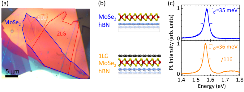
Figure 1(a) shows an optical image of our hBN-supported MoSe2/graphene sample deposited onto a Si/SiO2 substrate. The side view of the hBN/MoSe2 and hBN/MoSe2/1LG are sketched in Fig. 1(b) and typical room temperature PL spectra these two systems are shown in Fig. 1(c). The main PL peak slightly below 1.6 eV arises from the recombination of the lowest lying optically active MoSe2 exciton (, also known as the A-exciton) possibly with a minor contribution coming from the trion (charged exciton, ) Ross et al. (2013). The photophysics of this heterostructure is driven by the efficient energy transfer from the thermalized excitonic population towards the graphene layer, leading to strong PL quenching by about two orders of magnitude (see scaling factor in Fig. 1(c)). As an indirect consequence of the picosecond lifetime of the band-edge exciton, we observe a broad, high energy shoulder on the MoSe2/1LG PL spectrum that is assigned to hot luminescence from excited excitonic states, including Rydberg-like states from from the A-exciton manifold as well as the B-exciton (located near 190 meV above the band-edge A-exciton) Froehlicher et al. (2018). No sizeable hot PL signal is detected in the linear regime in the hBN-supported MoSe2 reference.
We now investigate the possibility of photoinduced charge transfer (i.e., photodoping) in the hBN/MoSe2/1LG region of our sample. As indicated above, band offsets between TMD and graphene allow electron and hole transfer from the TMD to graphene. Besides this intrinsic phenomenon, the presence of surface traps and molecular adsorbates (either on the substrate or on the 2D material) Ryu et al. (2010); Miller et al. (2015), as well as chalcogen vacancies and other local defects in TMDs Barja et al. (2019) can facilitate charge transfer and alter exciton dynamics. Under light illumination above the TMD bandgap, a net photoinduced charge transfer to graphene has been observed on SiO2-supported samples on timescales that are orders of magnitude longer than the TMD excitonic lifetime, hence with no sizeable effect on the PL intensity Froehlicher et al. (2018); Ahmed et al. (2020); Zhang et al. (2014). This photodoping leads to a stationary Fermi level shift in graphene and complementary fingerprints of charge transfer in the TMD monolayer Froehlicher et al. (2018); Lin et al. (2019). The Fermi level of graphene ultimately saturates as the photon flux increases Froehlicher et al. (2018); Lin et al. (2019). Although such extrinsic effects could be of practical use for photodetection Zhang et al. (2014); Ahmed et al. (2020), they may hamper access to the intrinsic photophysics of the heterostructure. In our sample, the bottom hBN flake provides a flat substrate that passivates the MoSe2/graphene heterostructure and could minimize extrinsic photodoping. Quantitative insights into photodoping can be obtained using micro-Raman spectroscopy Ferrari and Basko (2013) of the graphene flake.
Indeed, the presence of charge carriers in 1LG leads to well-documented changes in the frequency (), full-width at half maximum (FWHM, ) and intensity of its one-phonon G-mode (near ) due to the non-adiabatic renormalization of the Kohn anomaly at the point. Under moderate doping below , this effect leads to an electron-hole symmetric upshift of accompanied by a reduction of arising from the suppression of Landau damping Pisana et al. (2007); Yan et al. (2007); Froehlicher and Berciaud (2015). Similar, albeit less prominent effects are also observable in 2LG Yan et al. (2008). Contributions from doping can be disentangled from other perturbations, in particular due to built-in or applied strain, by inspecting the correlation between and the frequency of the 2D mode (near , involving a pair of near-zone edge phonons with opposite momenta Ferrari and Basko (2013)). The slope is near 2.2 under biaxial strain, directly reflecting the values of the Grüneisen parameters 2D- and G-mode phonons Lee et al. (2012); Metten et al. (2013, 2014) but is significantly smaller than 1 in the case of hole or electron doping (Fig. 2a) because the 2D-mode phonons have momenta significantly away from the Kohn anomaly at the zone edge (K and K’ points) Das et al. (2008); Froehlicher and Berciaud (2015).
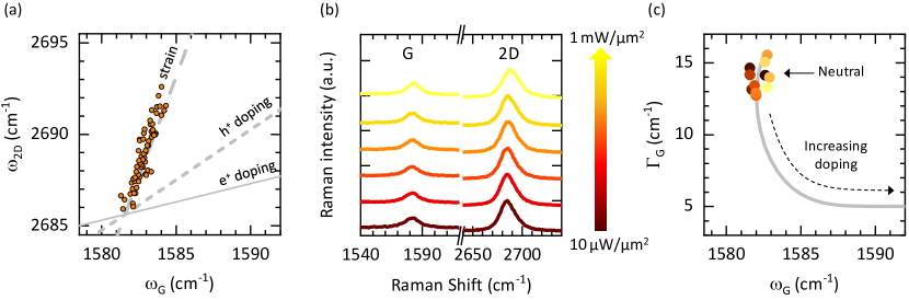
Figure 2(a) shows the correlation between and extracted from a Raman map of the monolayer MoSe2/1LG area of our sample (see Fig. 1a). Clearly, and follow a linear correlation with a slope near 2.2 (Fig. 2a), suggesting native compressive strain (i.e., stiffening of the Raman modes compared to the undoped/unstrained reference indicated in Fig. 2a) and ruling out sizable spatially inhomogeneous residual doping. The native strain level can be as large as (if one assumes biaxial strain Metten et al. (2014)) and the existence of a strain gradient likely arises from the stacking process. Figure 2(b) shows the evolution of the Raman spectra as a function of the incident laser intensity from up to . We observe that does not change appreciably and instead remains at . Similarly, remains constant around as it can be seen in figure 2(c). These values are typical for quasi-neutral graphene with a residual charge density of at most a few Froehlicher and Berciaud (2015). Hence, our observations strongly support the hypothesis that the hBN flake shields the heterostructure from substrate-induced electron redistribution and photo-doping, yielding a pristine system to investigate exciton dynamics.
III Low temperature hyperspectral PL mapping
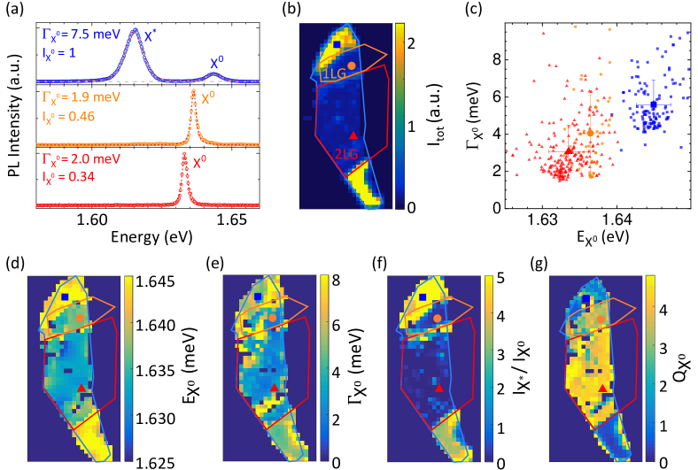
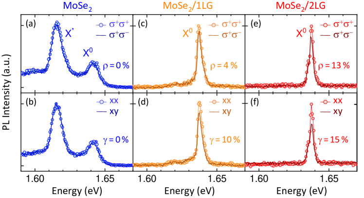
Figure 3a shows typical low temperature (14 K) PL spectra recorded on selected spots of our sample indicated in the PL intensity map shown in Fig. 3b. An hyperspectral PL mapping study is shown in Fig. 3c-g. On the MoSe2/hBN area, the PL spectrum is dominated by two main peaks located at eV and eV (Fig. 3c,d). These peaks have Voigt profiles and originate from the recombination of the neutral exciton () and the trion (), respectively Ross et al. (2013). In contrast, in the 1LG and 2LG-capped MoSe2 regions, the PL spectra display single, narrower quasi-Lorentzian emission lines (Fig. 3c,e). As shown in Fig. 3a,c,d, these peaks are located at eV for hBN/MoSe2/1LG and eV for hBN/MoSe2/2LG, respectively. These values are slightly redshifted by 9 and 12 meV with respect to the bare MoSe2 reference, respectively, due to dielectric screening Raja et al. (2017); Froehlicher et al. (2018).
Considering the simplicity of the PL-spectrum of bright TMDs such as MoSe2 Ross et al. (2013); Wang et al. (2018), the single-line character of the MoSe2/graphene PL spectra is essentially a consequence of the complete neutralization of the MoSe2 monolayer. As confirmed by Fig. 3a,f, the integrated PL intensity near the expected location of the feature is vanishingly small compared to that of line () over all the 1LG and 2LG-capped MoSe2 area.
The observed PL quenching, however, is a consequence of non-radiative energy transfer to graphene, stemming predominantly from hot excitons (either finite momentum excitons residing outside the light cone or excitons occupying higher-order optically active states), with a smaller contribution from cold excitons in the light cone Lorchat et al. (2020). As a result, the selected PL spectra in Fig. 3a and total PL intensity map (, Fig. 3b) reveal sizeable reduction of on the MoSe2/1LG and MoSe2/2LG regions. However, if we consider the quenching factor of the neutral exciton line only (denoted , see Fig. 3g), we observe a moderate on MoSe2/1LG and a slightly larger value of in the MoSe2/2LG, in qualitative agreement with previous studies of energy transfer from individual emitters to mono and few-layer graphene Chen et al. (2010). The reduced quenching efficiency compared to the massive quenching observed at room temperature stems from the picosecond radiative lifetime at low temperatures Robert et al. (2016); Fang et al. (2019), which is comparable to the energy transfer time to graphene (see Ref. Lorchat et al. (2020) for details).
Our spatially-resolved PL study also reveals narrow lines with spatially averaged FWHM () of and , on the MoSe2/1LG and MoSe2/2LG areas, respectively (Fig. 3c,e). Interestingly, gets as narrow as in selected locations (see Fig. 3e), a value that, even if it exceeds the homogeneous limit ( for an estimated lifetime of 2 ps) suggests that our simple sample architecture warrants reduced inhomogeneous broadening and dephasing, with values that are close to state of the art hBN-encapsulated MoSe2 samples Fang et al. (2019); Zhou et al. (2020). Figure 3(c) presents the correlation between and in each region of the sample, extracted from the maps in Fig. 3d,e. As expected, the presence of a second graphene layer improves capping and further screens the MoSe2 excitons.
Let us note that although our sample is spatially homogeneous over domains as large as 50 , we observe more scattered , larger and residual trion emission (Fig. 3d-g) near the boundaries of the 1LG and 2LG domains and also near localized micro-sized spots of our sample. During the stacking process, organic residues tend to segregate and form bubbles which locally decouple the TMD and graphene layers leading to complex spectra that reflect spatial inhomogeneities.
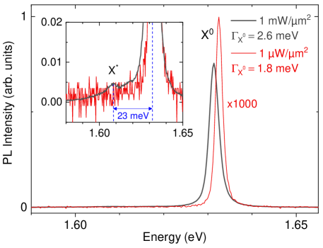
To close this section, let us comment on photoinduced doping at low-temperature. As indicated in Ref. Lorchat et al. (2020), TMD/graphene heterostructures are extremely photostable, in stark contrast with bare TMD monolayers. By illuminating our hBN/MoSe2/2LG sample at high laser intensity (), a dim photo-induced trion feature with a reduced binding energy of 23 meV emerges, with an integrated intensity nearly three orders of magnitude smaller than that of the line (Fig. 4). These results indicate that the MoSe2 layer coupled to graphene remains essentially neutral under intense cw illumination, and that one can safely neglect photo-induced doping, including at cryogenic temperatures.
IV Valley polarization and valley coherence
We finally address the valley contrasting properties of our sample. TMD/graphene heterostructures have recently been introduced as chiral emitters with large degrees of valley polarization () and coherence () up to room-temperature. Indeed, picosecond energy transfer between TMD and graphene allows the excitonic population to recombine before undergoing intervalley scattering and dephasing processes Lorchat et al. (2018); Paradisanos et al. (2020). In addition, graphene, as a capping material, reduces disorder, spatial inhomogeneities and dephasing, which explains the large room temperature value of recently reported in hBN-encapsulated WS2/1LG heterostructures Lorchat et al. (2018). Although improved valley contrasts come at the expense of strong PL quenching at room temperature, we expect, in keeping with the discussion above, that sizeable values of and combined with large emission yields can be achieved at lower temperatures.
Fig. 5 shows polarization-resolved PL spectra recorded using a circular and a linear basis, as well as the associated degrees of circular and linear polarization, which are directly yielding and , respectively. For the emission line, we get , and and , and for hBN-supported MoSe2, MoSe2/1LG and MoSe2/2LG, respectively.
Near-zero values of have been reported in MoSe2 monolayers Wang et al. (2015). Since the low temperature lifetimes in bare MoSe2 and in MoSe2/graphene heterostructures are similar Fang et al. (2019); Lorchat et al. (2020), the observation of modest values of in MoSe2/graphene is not surprising. Noteworthy, significantly exceeds in MoSe2/1LG and MoSe2/2LG, suggesting significantly reduced dephasing in encapsulated samples, as recently observed in MoS2 monolayers fully encapsulated in hBN Cadiz et al. (2017) and in hBN-capped WS2/1LG Lorchat et al. (2018). Here, our measurements are performed at 60 meV above the line. We anticipate larger values of and as we excite MoSe2/graphene samples closer to the resonance. In addition, one may also optimize the sample geometry as in Ref. Fang et al. (2019); Zhou et al. (2020) in order to minimize the radiative lifetime of the MoSe2 monolayer, and hence optimize and .
V Conclusion and perspectives
We have demonstrated that hBN-supported TMD/graphene heterostructures offer an excellent template to study electron redistribution and excitonic energy transfer in two dimensions, with donor-acceptor distances in the sub-nanometer range. The absence of photodoping in hBN-supported samples as compared to SiO2-supported systems adds on to the merits of hBN as an ideal dielectrics for van der Waals assembly. Our study also establishes that bright TMD emission with linewidths approaching the homogeneous limit can be achieved over large areas using only one epilayer of graphene, hence without the need of an hBN capping layer. In this manner, one does not only benefit from the emission filtering properties of graphene but also from its assets as a capping van der Waals material.
In spite of recent advances Froehlicher et al. (2018); Lorchat et al. (2020); Yuan et al. (2018); Aeschlimann et al. (2020); Selig et al. (2019) the microscopic details of the transfer mechanism are still under investigation. Focusing for instance on energy transfer, Dexter- and Förster-type mechanisms depend sensitively on the distance between the layers and on the local environment. Investigations of the transfer efficiency while finely tuning the TMD-graphene distance using hBN spacers and as a function of the number of graphene layers should bring decisive insights into near-field coupling in van der Waals materials.
Our work also holds promise for device-oriented research. Indeed, the absence of a top hBN layer allows us to directly contact the graphene electrode for photodetectors and light-emitting devices, as well as for local investigations, e.g., using scanning tunnelling microscopy Pommier et al. (2019). Conversely, TMDs have recently been shown to outperform hBN as a capping material, yielding record-high room temperature electron mobility in graphene Banszerus et al. (2019).
Finally, a challenging yet appealing perspective would consist in exploiting low-energy surface plasmon polaritons in graphene to tailor light-matter interactions in near-field coupled two-dimensional semiconductors Kurman et al. (2018), including in quantum wells made from the latter Schmidt et al. (2018).
VI Experimental details
Our van der Waals heterstructure was prepared using standard micromechanical exfoliation and dry transfer methods, as in ref Castellanos-Gomez et al. (2014). The hBN flake was mechanically exfoliated on top of the substrate. A MoSe2 monolayer and a single- and bilayer graphene flake were mechanically exfoliated from bulk crystals and then stacked on top of the hBN flake. The number of layers of the flakes were verified using room-temperature Raman and PL spectroscopy. PL and Raman scattering measurements in Figs. 1 and 2, respectively, were performed in ambient air using a 532 nm diode pumped solid state laser and a home-built scanning confocal setup. Low temperature PL studies were performed in a continuous-flow liquid helium cryostat mounted onto our Raman/PL microscope. All PL measurements in Fig. 3 were recorded in the linear regime under cw excitation at , i.e., slightly above the B exciton in MoSe2 Froehlicher et al. (2018); Wang et al. (2018). The low-temperature polarization-resolved measurements in Fig. 5 were performed under near-resonant optical excitation 60 meV above the neutral exciton () line using a tunable supercontinuum laser. The degree of valley polarization is measured in a circular basis and the degree of valley coherence is measured in a linear basis. In these expressions, indicates the PL intensity detected in the ”i” polarization state when upon excitation under ”j” polarized light (i,j= or x/y). A Linear polarizer and an achromatic quarter-waveplate were used to prepare the polarization state of the incoming beam. The emitted photons propagate through the same quarter-wave plate and are analyzed using a Wollaston prism, which permits to record simultaneously the co- and cross polarized PL signals. The values of and were determined from fits of the lines.
Acknowledgements
The authors thank X. Marie, C. Robert, D. Lagarde, S. Azzini, T. Chervy, C. Genet and G. Schull for fruitful discussions. We are grateful to Aditi Moghe and to the StNano clean room staff for technical support. We acknowledge financial support from the Agence Nationale de la Recherche (under grants 2D-POEM ANR-18-ERC1-0009) and from the LabEx NIE (ANR-11-LABX-0058-NIE, under grant SPE2D). A.S. and S.B. acknowledge support for the Indo-French Centre for the Promotion of Advanced Research (CEFIPRA). K.W. and T.T. acknowledge support from the Elemental Strategy Initiative conducted by the MEXT, Japan ,Grant Number JPMXP0112101001, JSPS KAKENHI Grant Number JP20H00354 and the CREST(JPMJCR15F3), JST.
References
- Mak et al. (2010) Kin Fai Mak, Changgu Lee, James Hone, Jie Shan, and Tony F. Heinz, “Atomically Thin : A New Direct-Gap Semiconductor,” Phys. Rev. Lett. 105, 136805 (2010).
- Splendiani et al. (2010) Andrea Splendiani, Liang Sun, Yuanbo Zhang, Tianshu Li, Jonghwan Kim, Chi-Yung Chim, Giulia Galli, and Feng Wang, “Emerging Photoluminescence in Monolayer ,” Nano Lett. 10, 1271–1275 (2010).
- Wang et al. (2018) Gang Wang, Alexey Chernikov, Mikhail M. Glazov, Tony F. Heinz, Xavier Marie, Thierry Amand, and Bernhard Urbaszek, “Colloquium: Excitons in atomically thin transition metal dichalcogenides,” Rev. Mod. Phys. 90, 021001 (2018).
- Goryca et al. (2019) M. Goryca, J. Li, A. V. Stier, T. Taniguchi, K. Watanabe, E. Courtade, S. Shree, C. Robert, B. Urbaszek, X. Marie, and S. A. Crooker, “Revealing exciton masses and dielectric properties of monolayer semiconductors with high magnetic fields,” Nature Communications 10, 4172 (2019).
- Xu et al. (2014) Xiaodong Xu, Wang Yao, Di Xiao, and Tony F. Heinz, “Spin and pseudospins in layered transition metal dichalcogenides,” Nat. Phys. 10, 343–350 (2014).
- Schaibley et al. (2016) John R Schaibley, Hongyi Yu, Genevieve Clark, Pasqual Rivera, Jason S Ross, Kyle L Seyler, Wang Yao, and Xiaodong Xu, “Valleytronics in 2D materials,” Nature Reviews Materials 1, 16055 (2016).
- Mak and Shan (2016) Kin Fai Mak and Jie Shan, “Photonics and optoelectronics of 2D semiconductor transition metal dichalcogenides,” Nat. Photonics 10, 216–226 (2016).
- Ciorciaro et al. (2020) Livio Ciorciaro, Martin Kroner, Kenji Watanabe, Takashi Taniguchi, and Atac Imamoglu, “Observation of magnetic proximity effect using resonant optical spectroscopy of an electrically tunable heterostructure,” Phys. Rev. Lett. 124, 197401 (2020).
- Lyons et al. (2020) T. P. Lyons, D. Gillard, A. Molina-Sánchez, A. Misra, F. Withers, P. S. Keatley, A. Kozikov, T. Taniguchi, K. Watanabe, K. S. Novoselov, J. Fernández-Rossier, and A. I. Tartakovskii, “Interplay between spin proximity effect and charge-dependent exciton dynamics in mose2/crbr3 van der waals heterostructures,” Nature Communications 11, 6021 (2020).
- Massicotte et al. (2016) M Massicotte, P Schmidt, F Vialla, KG Schädler, A Reserbat-Plantey, K Watanabe, T Taniguchi, KJ Tielrooij, and FHL Koppens, “Picosecond photoresponse in van der Waals heterostructures,” Nat. Nanotechnol. 11, 42–46 (2016).
- Luo et al. (2017) Yunqiu Kelly Luo, Jinsong Xu, Tiancong Zhu, Guanzhong Wu, Elizabeth J. McCormick, Wenbo Zhan, Mahesh R. Neupane, and Roland K. Kawakami, “Opto-valleytronic spin injection in monolayer MoS2/few-layer graphene hybrid spin valves,” Nano Lett. 17, 3877–3883 (2017).
- Avsar et al. (2017) Ahmet Avsar, Dmitrii Unuchek, Jiawei Liu, Oriol Lopez Sanchez, Kenji Watanabe, Takashi Taniguchi, Barbaros Özyilmaz, and Andras Kis, “Optospintronics in graphene via proximity coupling,” ACS Nano 11, 11678–11686 (2017).
- Castro Neto et al. (2009) A. H. Castro Neto, F. Guinea, N. M. R. Peres, K. S. Novoselov, and A. K. Geim, “The electronic properties of graphene,” Rev. Mod. Phys. 81, 109–162 (2009).
- Mak et al. (2012) Kin Fai Mak, Long Ju, Feng Wang, and Tony F Heinz, “Optical spectroscopy of graphene: from the far infrared to the ultraviolet,” Solid State Commun. 152, 1341–1349 (2012).
- Lorchat et al. (2018) Etienne Lorchat, Stefano Azzini, Thibault Chervy, Takashi Taniguchi, Kenji Watanabe, Thomas W Ebbesen, Cyriaque Genet, and Stéphane Berciaud, “Room-temperature valley polarization and coherence in transition metal dichalcogenide–graphene van der waals heterostructures,” ACS Photonics 5, 5047 (2018).
- He et al. (2014) Jiaqi He, Nardeep Kumar, Matthew Z Bellus, Hsin-Ying Chiu, Dawei He, Yongsheng Wang, and Hui Zhao, “Electron transfer and coupling in graphene–tungsten disulfide van der Waals heterostructures,” Nat. Commun. 5, 5622 (2014).
- Froehlicher et al. (2018) Guillaume Froehlicher, Etienne Lorchat, and Stéphane Berciaud, “Charge versus energy transfer in atomically thin graphene-transition metal dichalcogenide van der waals heterostructures,” Phys. Rev. X 8, 011007 (2018).
- Yuan et al. (2018) Long Yuan, Ting-Fung Chung, Agnieszka Kuc, Yan Wan, Yang Xu, Yong P. Chen, Thomas Heine, and Libai Huang, “Photocarrier generation from interlayer charge-transfer transitions in WS2-graphene heterostructures,” Science Advances 4, e1700324 (2018).
- Selig et al. (2019) Malte Selig, Ermin Malic, Kwang Jun Ahn, Norbert Koch, and Andreas Knorr, “Theory of optically induced Förster coupling in van der Waals coupled heterostructures,” Phys. Rev. B 99, 035420 (2019).
- Robert et al. (2016) C. Robert, D. Lagarde, F. Cadiz, G. Wang, B. Lassagne, T. Amand, A. Balocchi, P. Renucci, S. Tongay, B. Urbaszek, and X. Marie, “Exciton radiative lifetime in transition metal dichalcogenide monolayers,” Phys. Rev. B 93, 205423 (2016).
- Fang et al. (2019) H. H. Fang, B. Han, C. Robert, M. A. Semina, D. Lagarde, E. Courtade, T. Taniguchi, K. Watanabe, T. Amand, B. Urbaszek, M. M. Glazov, and X. Marie, “Control of the exciton radiative lifetime in van der waals heterostructures,” Phys. Rev. Lett. 123, 067401 (2019).
- Lorchat et al. (2020) Etienne Lorchat, Luis E. Parra López, Cédric Robert, Delphine Lagarde, Guillaume Froehlicher, Takashi Taniguchi, Kenji Watanabe, Xavier Marie, and Stéphane Berciaud, “Filtering the photoluminescence spectra of atomically thin semiconductors with graphene,” Nature Nanotechnology 15, 283–288 (2020).
- Yu et al. (2009) Young-Jun Yu, Yue Zhao, Sunmin Ryu, Louis E Brus, Kwang S Kim, and Philip Kim, “Tuning the graphene work function by electric field effect,” Nano Lett. 9, 3430–3434 (2009).
- Liang et al. (2013) Yufeng Liang, Shouting Huang, Ryan Soklaski, and Li Yang, “Quasiparticle band-edge energy and band offsets of monolayer of molybdenum and tungsten chalcogenides,” Appl. Phys. Lett. 103, 042106 (2013).
- Wilson et al. (2017) Neil R. Wilson, Paul V. Nguyen, Kyle Seyler, Pasqual Rivera, Alexander J. Marsden, Zachary P. L. Laker, Gabriel C. Constantinescu, Viktor Kandyba, Alexei Barinov, Nicholas D. M. Hine, Xiaodong Xu, and David H. Cobden, “Determination of band offsets, hybridization, and exciton binding in 2D semiconductor heterostructures,” Science Advances 3, e1601832 (2017).
- Hill et al. (2017) Heather M. Hill, Albert F. Rigosi, Archana Raja, Alexey Chernikov, Cyrielle Roquelet, and Tony F. Heinz, “Exciton broadening in WS2/graphene heterostructures,” Phys. Rev. B 96, 205401 (2017).
- Ryu et al. (2010) Sunmin Ryu, Li Liu, Stéphane Berciaud, Young-Jun Yu, Haitao Liu, Philip Kim, George W. Flynn, and Louis E. Brus, “Atmospheric oxygen binding and hole doping in deformed graphene on a SiO2 substrate,” Nano Lett. 10, 4944–4951 (2010).
- Miller et al. (2015) Bastian Miller, Eric Parzinger, Anna Vernickel, Alexander W Holleitner, and Ursula Wurstbauer, “Photogating of mono-and few-layer MoS2,” Appl. Phys. Lett. 106, 122103 (2015).
- Lin et al. (2019) Weiyi Lin, Pingping Zhuang, Harry Chou, Yuqian Gu, Richard Roberts, Wei Li, Sanjay K. Banerjee, Weiwei Cai, and Deji Akinwande, “Electron redistribution and energy transfer in graphene/mos2 heterostructure,” Applied Physics Letters 114, 113103 (2019).
- Dean et al. (2010) Cory R Dean, Andrea F Young, Inanc Meric, Chris Lee, Lei Wang, S Sorgenfrei, K Watanabe, T Taniguchi, P Kim, KL Shepard, et al., “Boron nitride substrates for high-quality graphene electronics,” Nat. Nanotechnol. 5, 722–726 (2010).
- Cadiz et al. (2017) F. Cadiz, E. Courtade, C. Robert, G. Wang, Y. Shen, H. Cai, T. Taniguchi, K. Watanabe, H. Carrere, D. Lagarde, M. Manca, T. Amand, P. Renucci, S. Tongay, X. Marie, and B. Urbaszek, “Excitonic linewidth approaching the homogeneous limit in MoS2-based van der waals heterostructures,” Phys. Rev. X 7, 021026 (2017).
- Ajayi et al. (2017) Obafunso A Ajayi, Jenny V Ardelean, Gabriella D Shepard, Jue Wang, Abhinandan Antony, Takeshi Taniguchi, Kenji Watanabe, Tony F Heinz, Stefan Strauf, X-Y Zhu, and James C Hone, “Approaching the intrinsic photoluminescence linewidth in transition metal dichalcogenide monolayers,” 2D Materials 4, 031011 (2017).
- Back et al. (2018) Patrick Back, Sina Zeytinoglu, Aroosa Ijaz, Martin Kroner, and Atac Imamoğlu, “Realization of an electrically tunable narrow-bandwidth atomically thin mirror using monolayer ,” Phys. Rev. Lett. 120, 037401 (2018).
- Scuri et al. (2018) Giovanni Scuri, You Zhou, Alexander A. High, Dominik S. Wild, Chi Shu, Kristiaan De Greve, Luis A. Jauregui, Takashi Taniguchi, Kenji Watanabe, Philip Kim, Mikhail D. Lukin, and Hongkun Park, “Large excitonic reflectivity of monolayer encapsulated in hexagonal boron nitride,” Phys. Rev. Lett. 120, 037402 (2018).
- Zhou et al. (2020) You Zhou, Giovanni Scuri, Jiho Sung, Ryan J. Gelly, Dominik S. Wild, Kristiaan De Greve, Andrew Y. Joe, Takashi Taniguchi, Kenji Watanabe, Philip Kim, Mikhail D. Lukin, and Hongkun Park, “Controlling excitons in an atomically thin membrane with a mirror,” Phys. Rev. Lett. 124, 027401 (2020).
- Wang et al. (2015) G. Wang, E. Palleau, T. Amand, S. Tongay, X. Marie, and B. Urbaszek, “Polarization and time-resolved photoluminescence spectroscopy of excitons in monolayers,” Appl. Phys. Lett. 106, 112101 (2015).
- Kioseoglou et al. (2016) G. Kioseoglou, A. T. Hanbicki, M. Currie, A. L. Friedman, and B. T. Jonker, “Optical polarization and intervalley scattering in single layers of MoS and MoSe,” Scientific Reports 6, 25041 (2016).
- Ross et al. (2013) Jason S Ross, Sanfeng Wu, Hongyi Yu, Nirmal J Ghimire, Aaron M Jones, Grant Aivazian, Jiaqiang Yan, David G Mandrus, Di Xiao, Wang Yao, et al., “Electrical control of neutral and charged excitons in a monolayer semiconductor,” Nat. Commun. 4, 1474 (2013).
- Barja et al. (2019) Sara Barja, Sivan Refaely-Abramson, Bruno Schuler, Diana Y. Qiu, Artem Pulkin, Sebastian Wickenburg, Hyejin Ryu, Miguel M. Ugeda, Christoph Kastl, Christopher Chen, Choongyu Hwang, Adam Schwartzberg, Shaul Aloni, Sung-Kwan Mo, D. Frank Ogletree, Michael F. Crommie, Oleg V. Yazyev, Steven G. Louie, Jeffrey B. Neaton, and Alexander Weber-Bargioni, “Identifying substitutional oxygen as a prolific point defect in monolayer transition metal dichalcogenides,” Nature Communications 10, 3382 (2019).
- Ahmed et al. (2020) Tanweer Ahmed, Kallol Roy, Saloni Kakkar, Avradip Pradhan, and Arindam Ghosh, “Interplay of charge transfer and disorder in optoelectronic response in graphene/hBN/MoS2 van der waals heterostructures,” 2D Materials 7, 025043 (2020).
- Zhang et al. (2014) Wenjing Zhang, Chih-Piao Chuu, Jing-Kai Huang, Chang-Hsiao Chen, Meng-Lin Tsai, Yung-Huang Chang, Chi-Te Liang, Yu-Ze Chen, Yu-Lun Chueh, Jr-Hau He, Mei-Yin Chou, and Lain-Jong Li, “Ultrahigh-Gain Photodetectors Based on Atomically Thin Graphene- Heterostructures,” Sci. Rep. 4 3826 (2014), 10.1038/srep03826.
- Ferrari and Basko (2013) Andrea C. Ferrari and Denis M. Basko, “Raman spectroscopy as a versatile tool for studying the properties of graphene,” Nat. Nanotechnol. 8, 235–246 (2013).
- Pisana et al. (2007) Simone Pisana, Michele Lazzeri, Cinzia Casiraghi, Kostya S. Novoselov, A. K. Geim, Andrea C. Ferrari, and Francesco Mauri, “Breakdown of the adiabatic born-oppenheimer approximation in graphene,” Nat. Mater. 6, 198–201 (2007).
- Yan et al. (2007) Jun Yan, Yuanbo Zhang, Philip Kim, and Aron Pinczuk, “Electric field effect tuning of electron-phonon coupling in graphene,” Phys. Rev. Lett. 98, 166802 (2007).
- Froehlicher and Berciaud (2015) Guillaume Froehlicher and Stéphane Berciaud, “Raman spectroscopy of electrochemically gated graphene transistors: Geometrical capacitance, electron-phonon, electron-electron, and electron-defect scattering,” Phys. Rev. B 91, 205413 (2015).
- Yan et al. (2008) Jun Yan, Erik Henriksen, Philip Kim, and Aron Pinczuk, “Observation of anomalous phonon softening in bilayer graphene,” Phys. Rev. Lett. 101, 136804 (2008).
- Lee et al. (2012) Ji Eun Lee, Gwanghyun Ahn, Jihye Shim, Young Sik Lee, and Sunmin Ryu, “Optical separation of mechanical strain from charge doping in graphene,” Nat. Commun. 3, 1024 (2012).
- Metten et al. (2013) Dominik Metten, François Federspiel, Michelangelo Romeo, and Stéphane Berciaud, “Probing built-in strain in freestanding graphene monolayers by Raman spectroscopy,” physica status solidi (b) 250, 2681–2686 (2013).
- Metten et al. (2014) Dominik Metten, François Federspiel, Michelangelo Romeo, and Stéphane Berciaud, “All-optical blister test of suspended graphene using micro-Raman spectroscopy,” Phys. Rev. Appl 2, 054008 (2014).
- Das et al. (2008) A. Das, S. Pisana, B. Chakraborty, S. Piscanec, S. K. Saha, U. V. Waghmare, K. S. Novoselov, H. R. Krishnamurthy, A. K. Geim, A. C. Ferrari, and A. K. Sood, “Monitoring dopants by Raman scattering in an electrochemically top-gated graphene transistor,” Nat. Nanotechnol. 3, 210–215 (2008).
- Raja et al. (2017) Archana Raja, Andrey Chaves, Jaeeun Yu, Ghidewon Arefe, Heather M. Hill, Albert F. Rigosi, Timothy C. Berkelbach, Philipp Nagler, Christian Schüller, Tobias Korn, Colin Nuckolls, James Hone, Louis E. Brus, Tony F. Heinz, David R. Reichman, and Alexey Chernikov, “Coulomb engineering of the bandgap and excitons in two-dimensional materials,” Nature Communications 8, 15251 (2017).
- Chen et al. (2010) Zheyuan Chen, Stéphane Berciaud, Colin Nuckolls, Tony F Heinz, and Louis E Brus, “Energy transfer from individual semiconductor nanocrystals to graphene,” ACS Nano 4, 2964–2968 (2010).
- Paradisanos et al. (2020) I. Paradisanos, K. M. McCreary, D. Adinehloo, L. Mouchliadis, J. T. Robinson, Hsun-Jen Chuang, A. T. Hanbicki, V. Perebeinos, B. T. Jonker, E. Stratakis, and G. Kioseoglou, “Prominent room temperature valley polarization in WS2/graphene heterostructures grown by chemical vapor deposition,” Applied Physics Letters 116, 203102 (2020).
- Aeschlimann et al. (2020) Sven Aeschlimann, Antonio Rossi, Mariana Chávez-Cervantes, Razvan Krause, Benito Arnoldi, Benjamin Stadtmüller, Martin Aeschlimann, Stiven Forti, Filippo Fabbri, Camilla Coletti, and Isabella Gierz, “Direct evidence for efficient ultrafast charge separation in epitaxial WS2/graphene heterostructures,” Science Advances 6, eaay0761 (2020), 10.1126/sciadv.aay0761.
- Pommier et al. (2019) Delphine Pommier, Rémi Bretel, Luis E. Parra López, Florentin Fabre, Andrew Mayne, Elizabeth Boer-Duchemin, Gérald Dujardin, Guillaume Schull, Stéphane Berciaud, and Eric Le Moal, “Scanning tunneling microscope-induced excitonic luminescence of a two-dimensional semiconductor,” Phys. Rev. Lett. 123, 027402 (2019).
- Banszerus et al. (2019) L Banszerus, T Sohier, A Epping, F Winkler, F Libisch, F Haupt, K Watanabe, T Taniguchi, K Müller-Caspary, N Marzari, et al., “Extraordinary high room-temperature carrier mobility in graphene-WSe heterostructures,” arXiv preprint arXiv:1909.09523 (2019).
- Kurman et al. (2018) Yaniv Kurman, Nicholas Rivera, Thomas Christensen, Shai Tsesses, Meir Orenstein, Marin Soljačić, John D. Joannopoulos, and Ido Kaminer, “Control of semiconductor emitter frequency by increasing polariton momenta,” Nature Photonics 12, 423–429 (2018).
- Schmidt et al. (2018) Peter Schmidt, Fabien Vialla, Simone Latini, Mathieu Massicotte, Klaas-Jan Tielrooij, Stefan Mastel, Gabriele Navickaite, Mark Danovich, David A. Ruiz-Tijerina, Celal Yelgel, Vladimir Fal’ko, Kristian S. Thygesen, Rainer Hillenbrand, and Frank H. L. Koppens, “Nano-imaging of intersubband transitions in van der waals quantum wells,” Nature Nanotechnology 13, 1035–1041 (2018).
- Castellanos-Gomez et al. (2014) Andres Castellanos-Gomez, Michele Buscema, Rianda Molenaar, Vibhor Singh, Laurens Janssen, Herre S J van der Zant, and Gary A Steele, “Deterministic transfer of two-dimensional materials by all-dry viscoelastic stamping,” 2D Mater. 1, 011002 (2014).