Effects of parallel electric and magnetic fields on Rydberg excitons in buckled two-dimensional materials.
Abstract
We study direct and indirect magnetoexcitons in Rydberg states in monolayers and double-layer heterostructures of Xenes (silicene, germanene, and stanene) in external parallel electric and magnetic fields, applied perpendicular to the monolayer and heterostructure. We calculate binding energies of magnetoexcitons for the Rydberg states, 1, 2, 3, and 4, by numerical integration of the Schrödinger equation using the Rytova-Keldysh potential for direct and both the Rytova-Keldysh and Coulomb potentials for indirect magnetoexcitons, respectively. Latter allows understanding a role of screening in Xenes. In the external perpendicular electric field, the buckled structure of the Xene monolayers leads to appearance of potential difference between sublattices allowing to tune electron and hole masses and, therefore, the binding energies and diamagnetic coefficients (DMCs) of magnetoexcitons. We report the energy contribution from electric and magnetic fields to the binding energies and DMCs. The tunability of the energy contribution of direct and indirect magnetoexcitons by electric and magnetic fields is demonstrated. It is also shown that DMCs of direct excitons can be tuned by the electric field, and the DMCs of indirect magnetoexcitons can be tuned by the electric field and manipulated by the number of hBN layers. Therefore, allowing the possibility of electronic devices design that can be controlled by external electric and magnetic fields and the number of hBN layers. The calculations of the binding energies and DMCs of magnetoexcitons in Xenes monolayers and heterostructures are novel and can be compared with the experimental results when they will be available.
I Introduction
After graphene monolayer was successfully isolated and identified in 2004 Novoselov2004 , the rapid study of fundamental properties and applications in nano- and quantum devices of two dimensional materials has begun (Mcdonell2016, ; Novoselov2016, ; Heerema2016, ; Iannaccone2018, ). Initially, the main focus was graphene that led to the current vast body of knowledge about the structure, electric, magnetic, and transport properties of graphene (CastroNeto2009a, ; Avouris2017, ). Despite its uniqueness, graphene has a closed energy gap at / points of the Brillouin zone complicating its application in electronics. As a result, the search and study of other 2D materials are underway.
Transition-metal dichalcogenides (TMDCs) and Xenes monolayers are among the main focus of the current research since TMDCs have the direct energy gap and Xenes have the energy gap that can be opened by the perpendicular electric field at / points that can be utilized in the electronics. In this paper, we adopt Xenes definition given in Ref. Molle2017 ; Zheng2020 . Xenes is a general name given to 2D buckled materials formed by elements from XIV group (First Generation Grazianetti2019 ): silicene (Si), germanene (Ge), and stanene (Sn). In contrast to graphene, other elements from XIV group have the most stable monolayer form when atoms are arranged in the honeycomb pattern where lattices A and B are offset with respect to the plane of the monolayer (Matthesparam, ; Molle2017, ). The offset between latices is called the buckling constant or buckling factor, . This unique structure of Xenes makes monolayers sensitive to the external electric field applied perpendicular to the monolayer allowing to control the band gap size.
The influence of the magnetic field on the excitonic wave function and binding energy of the exciton is well established. Excitons in a bulk, double quantum wells or 2D structures in the presence of the magnetic field result in a possible formation in these structures of quasiparticles called magnetoexcitons. Magnetoexcitons in TMDCs monolayers present a great interest since the binding energy of the magnetoexcitons can be tuned by the perpendicular to the monolayer magnetic field. On one hand, magnetoexcitons in TMDCs monolayers have been extensively studied in the past few years. For example, the exciton binding energies for Rydberg states are reported in Refs. (Liu2019, ; Koperski, ; Stier_2016, ; Aivazian, ; Chen2019, ; Gor2019, ; Macneill, ; Striv, ; Ludwig, ; Plechinger, ; Zipfel, ; Kidd, ; Mayers, ; Goldstein, ; Robert, ; Liu_2020, ; Arora, ), the Zeeman shift has been considered in Refs. (DonckDM2018, ; Koperski, ; Stier_2016, ; Aivazian, ; Chen2019, ; Rybkovkiy, ; Gor2019, ; Macneill, ; Liu2019, ; Striv, ; Ludwig, ; Plechinger, ; Spiridonova, ; Stier2018, ), while the diamagnetic shift was addressed in Refs. (DonckDM2018, ; Liu2019, ; Stier_2016, ; Aivazian, ; Gor2019, ; Macneill, ; Plechinger, ; Stier2018, ; Luckert, ; donckexc, ; Choi2015, ; Walck, ; Han2018, ; Zipfel, ; Spiridonova, ). On the other hand, there is a lack of research on magnetoexcitons in Xenes monolayers since the synthesis of Xenes monolayers has not been very successful compared to TMDCs because of Xenes instability in the air Tao2015 . In contrast to graphene, silicene monolayers do not occur in nature. However, silicene nanoribons were experimentally synthesized on a metal substrate (Aufray2010, ; Padova2010, ) that opened the way for silicene, germanene, and stanene monolayers being transferred on metal (Drummond2012, ; Saxena2016, ; Davila2014, ; Mannix2017, ; Grazianetti2019, ) and an insulating substrate such as MoS2 Sante2019 and hexagonal boron nitride (hBN) (LiWang2013, ; Khan2017, ). Depositing Xenes on a metallic substrate is easier. For example, silicene can be grown on Ag (111) (Tao2015, ; Ezawa1, ) or germanene synthesis by dry deposition on Au (111) surface Davila2014 . However, depositing Xene on a metal significantly alters properties of the Xene monolayer. Depositing Xenes on hBN is harder, but hBN preserves properties of the Xenes since Xenes and hBN weakly interact LiWang2013 . Properties of Xenes on different substrates are presented in Refs. Molle2017 ; LiWang2013 .
Nevertheless, magnetoexcitons in Xenes present a great interest for fundamental research and application in electronic devices. Out of all Xenes, silicene is most studied Zhao2016 . Due to Xenes monolayer unique buckling structure, electron-hole masses depend on the band gap that in return depends on the perpendicular to the monolayer electric field. Since the exciton binding energy depends on the reduced mass of the exciton, by applying the electric field the exciton binding energy can be tuned.
Optical properties of Xenes have been addressed in Refs. (Matthesparam, ; Bechstedt2012, ; Fadaie2016, ; Stille2012, ), and magneto-optical properties are studied in Ref. Muoi2020 ; Chowdhury2016 . Hall effect Ezawa1 , the valley-locked spin-dependent Seeback effect Zhai2018 , anomalous quantum Hall effect Ezawa2 , and quantum spin Hall effect Zhao2020 are being addressed since they are essential for the use of Xenes in nano- and quantum devices (Glavin2020, ; Lyu2019, ; Tao2020, ; Chen2018, ; Zhao2020, ). Currently, there is a lack of studies on magnetoexciton binding energies, Zeeman shift, and diamagnetic coefficients (DMCs) in Xenes monolayers. However, the Landau levels have been addressed in Refs. (Ezawa1, ; Muoi2020, ; Tsaran2014, ). Moreover, a particular interest presents the study of magnetoexcitons formation in a double-layer structure of Xenes separated by layers of hBN. In such system electrons are confined in one Xene monolayer, while an equal number of positive holes are located in a parallel Xene monolayer at a distance away. Thus, the electron and hole are spatially separated by a dielectric. The system of the charge carriers in two parallel Xenes layers can be treated as a two-dimensional system without interlayer hopping. In this system, the electron-hole recombination due to the tunneling of electrons and holes between different Xenes monolayers is suppressed by the dielectric barrier produced by hBN monolayers that separates the Xenes monolayers. Therefore, the indirect (dipolar) excitons, formed by electrons and holes, located in two different Xenes monolayers, have a longer lifetime than the direct magnetoexcitons Lozovik1976 . In the past 6 years binding energies of Rydberg states of excitons in TMDCs monolayers and heterostructures in the magnetic field have been intensively studied experimentally and theoretically (Liu2019, ; Koperski, ; Stier_2016, ; Aivazian, ; Chen2019, ; Gor2019, ; Macneill, ; Striv, ; Ludwig, ; Plechinger, ; Zipfel, ; Kidd, ; Mayers, ; Goldstein, ; Robert, ; Liu_2020, ; Arora, ), and the diamagnetic shifts were considered in Refs. (DonckDM2018, ; Liu2019, ; Stier_2016, ; Aivazian, ; Gor2019, ; Macneill, ; Plechinger, ; Stier2018, ; Luckert, ; donckexc, ; Choi2015, ; Walck, ; Han2018, ; Zipfel, ; Spiridonova, ). This motivates us to focus our study solely on the Rydberg states of excitons in Xenes in the magnetic field.
In this paper, we study the dependence of the magnetoexciton binding energy of Rydberg states, 1, 2, 3, and 4, on the perpendicular to the monolayer electric and magnetic fields and calculate the diamagnetic coefficients for (i) the direct magnetoexcitons in Xenes monolayers and (ii) for the indirect magnetoexcitons in Xenes heterostructure formed by two monolayers of the same Xene and separated by monolayers of hBN. The heterostructure is denoted as X-hBN-X, and the number of hBN layers is varied between 1 and 6. We numerically solve the Schrödinger equation for the magnetoexciton in external electric and magnetic fields to obtain eigenfunctions and eigenvalues. Then we calculate the energy contribution from the magnetic field to the binding energy, as well as its dependence on the applied electric field. From the energy contribution from the magnetic field to the binding energy, we extract the DMCs. For the direct exciton, we solve the Schrödinger equation with the Rytova-Keldysh potential (Rytova, ; Keldysh, ), and for the indirect exciton, we solve the Schrödinger equation with the Rytova-Kyldysh and the Coulomb potentials. This allows to understand the role of screening in Xenes. So, we study the dependence of the binding energy of indirect magnetoexcitons on the external electric and magnetic fields, as well as on the separation of the Xenes layers by the layers of hBN. The calculations of the binding energies of magnetoexcitons and DMCs in Xenes monolayers and heterostructure are reported for the first time. As a result, our study demonstrate a tunability of the energy contribution of direct and indirect magnetoexcitons by electric and magnetic fields. It is shown that DMCs of direct excitons can be tuned by the electric field, while the DMCs of indirect magnetoexcitons can be tuned by the electric field and manipulated by the number of hBN layers. Therefore, we demonstrate a possibility of electronic devices design that can be controlled by the external electric and magnetic fields and the number of hBN layers.
The paper is organized in the following way. In Sec. II is given the theoretical formalism for the description of an electron and hole in buckled 2D materials. Here we present the effective mass approach for magnetoexcitons in buckled 2D materials and the Schrödinger equation for the exciton in parallel electric and magnetic fields, which are perpendicular to the Xene monolayer. The theoretical consideration of indirect magnetoexcitons in Xenes heterostructure is given in Subsec. II.3. The results of calculations of the energy contribution from the electric and magnetic fields to the binding energy and diamagnetic shifts of the direct and indirect magnetoexcitons and dependence of the energy contribution and diamagnetic shifts for indirect magnetoexcitons in Xenes heterostructures on the number of hBN layers on the external electric field are presented in Sec. III. Conclusions follow in Sec. IV.
II Theoretical Formalism
II.1 Electron and hole in buckled 2D materials
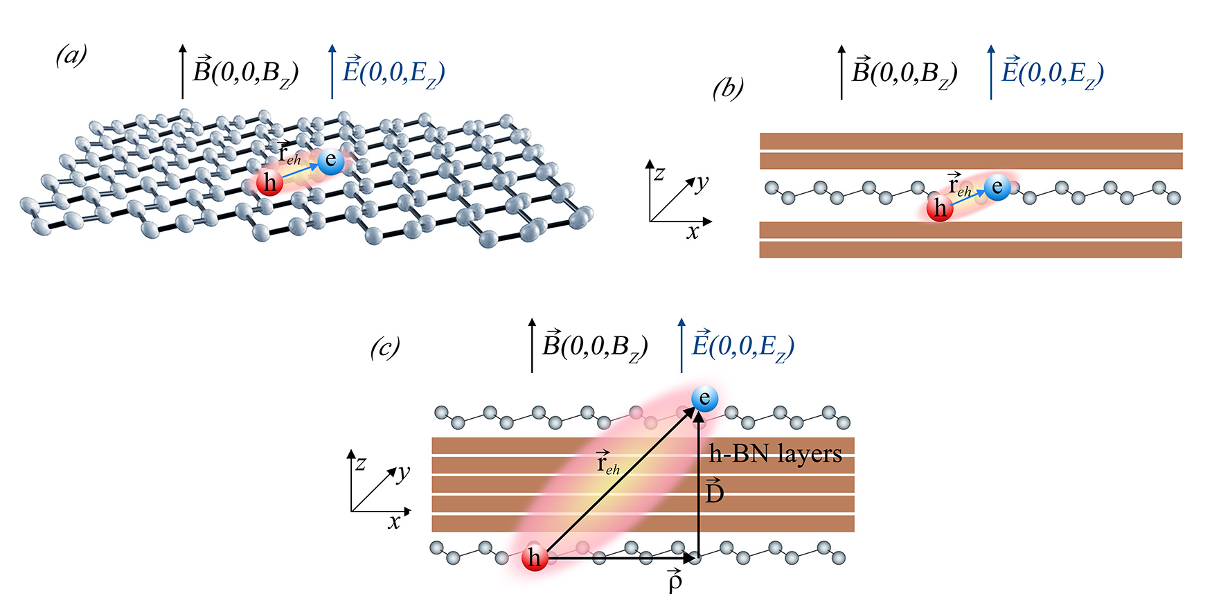
Let us provide an outline of the low-energy model that describes excitons states in Xenes monolayers and heterostructures under applied electric and magnetic fields. We are considering an electron and hole in parallel magnetic and electric fields, which are perpendicular to a Xene monolayer or heterostructure as it is shown in Fig. 1. Monolayers of silicene, germanene, and low-buckled stanene can be pictured as honeycomb graphene monolayers but have an out of plane buckling such that the A and B triangular sublattices are offset with respect to the plane of the monolayer and separated by a distance . This distance is known as the buckling constant or buckling factor. The intrinsic sensitivity of Xenes to an external electric field applied perpendicular to the plane of the monolayer is mounted due to the offset between the two triangular sublattices. In particular, this asymmetry causes an on-site potential difference to occur between sublattices when an out-of-plane electric field is applied. The band structure of Xenes in the vicinity of the points resembles graphene when there is no external electric field; though, the intrinsic gaps of Xenes are significantly larger than that of graphene. The application of a perpendicular electric field creates a potential difference between the sublattices, causing a change in the band gap in the monolayer Xenes, which in turn changes the effective masses of the electrons and holes.
The single-particle spectrum of electronic states in monolayer Xenes in the electric field acting along the -axis in the vicinity of the points is described by a two-dimensional (2D) massive Dirac Hamiltonian is given in Ref. Tabert as (:
| (1) |
In Hamiltonian (1) is the Fermi velocity, and are the components of momentum in the monolayer -plane, relative to the points, and are the pseudospin and real spin Pauli matrices, respectively, is the intrinsic band gap, are the valley and spin indices, respectively, and is the gap induced by the external electric field , acting along the -axis, where in the latter expression is the buckling constant. As it follows from Refs. Ezawa2 ; Tabert ; Ezawa3 , Hamiltonian (1), which describe electronic states in Xenes, is analogous to the 2D Dirac Hamiltonian for TMDCs monolayers. The first term in Eq. (1) is the same as that of the low-energy Hamiltonian in graphene CastroNeto2009a ; Abergel2010 . The last term in (1) describes the sublattice potential difference that could arise from the application of a perpendicular electric field Drummond2012 ; Ezawa1 ; Ezawa2 ; Ezawa3 , while the spin-orbit coupling Kane2005 with an intrinsic band gap of is given by the second term. The Hamiltonian for the single-particle spectrum of electronic states in monolayer Xenes can be obtained by replacing , where is the vector potential such that , where is the magnetic field.
Using Eq. (1) one may write the low-energy eigenvalues for charge carriers near the points as Tabert :
| (2) |
where
| (3) |
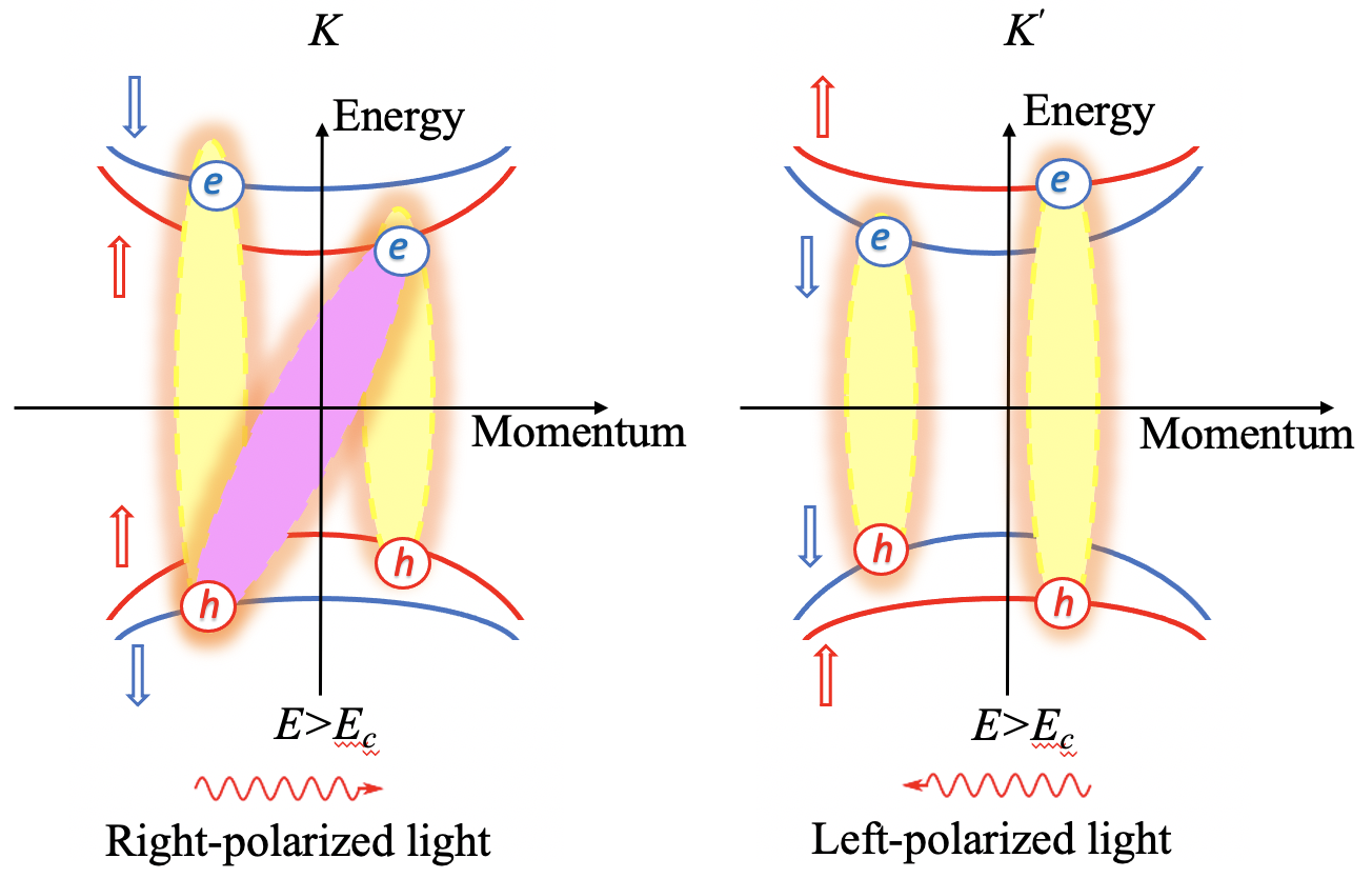
is the electric field-dependent band gap at . We note that when , the spin-up and spin-down bands of the valence and conduction bands are degenerate. In other words, spin-orbit splitting only manifests itself at non-zero external electric fields. At non-zero electric fields, both the valence and conduction bands split, into upper bands with a large gap (when ), and lower bands with a small gap (when ). We call the excitons formed by charge carriers from the large gap excitons, and those formed by charge carriers in the small gap excitons. The direct bright and excitons consist of the electron and hole with parallel spins (Echeverry2016, ; Malic2018, ). There exist two additional states when the electron and hole have antiparallel spins, but these excitons are optically forbidden and called spin forbidden dark excitons. The schematic band structure of and excitons formation in and valleys under the right- and left-polarized light, respectively, is given in Fig. 2. Following Ezawa Ezawa3 , we show the case when the applied perpendicular electric field is bigger than the critical value of the electric field, . When the external field reaches a critical value , the lower bands form a Dirac cone at the points. The corresponding values of the critical electric field for monolayer Xenes are given in Ref. BBKPRB2019 . The conduction and valence bands are parabolic in the vicinity of the points. One can find the effective mass of charge carriers near the points as (Pan2015, ; Matthesparam, ). The effective masses of electrons and holes are the same due to the symmetry between the lowest conduction and highest valence bands, and can be written as a function of the external electric field in the following form:
| (4) |
Therefore, it is worth mentioning that the reduced mass of an exciton in Xenes is a function of the external electric field for and excitons. Following ab initio calculations Drummond2012 , which determined that the crystal structure of silicene becomes unstable around 2.6 V/Å, we consider in our calculations external electric fields up to 2.7 V/Å. Analysis of Eq. (4) shows that the value of reduced mass depends on the band gap, Fermi velocity, and buckling constant. For example, for freestanding silicene, germanene, and stanene 2 is 1.9 (1.55) meV Matthesparam (LiuFeng2011 ), 33 (23.9) meV Matthesparam (LiuFeng2011 ), and 101 (73.5) meV Matthesparam (Liu2011 ), while the corresponding Fermi velocities are 6.5 (5.3)105 m/s Matthesparam (Matthes2013 ), 6.2 (5.2)105 m/s Matthesparam (Matthes2013 ), and 5.5 (4.8 )105 m/s Matthesparam (Liu2011 ). Let us notice that the citations in parenthesis are related to the data in parentheses. At small electric fields, germanene and especially stanene show significant differences between the reduced masses of the and excitons. The latter is due to their large intrinsic band gaps. Silicene, which has an intrinsic band gap on the order of a couple of meV, exhibits very little difference between the reduced masses of and excitons, even at relatively small electric fields. At large electric field the difference between the and exciton reduced mass is negligible in silicene and germanene. In all cases, the mass of the exciton exceeds the mass of the exciton.
II.2 Effective mass approach for magnetoexcitons in buckled 2D materials
Excitonic systems are many-body systems, and the most systematic approach requires the use of quantum field theory. However, these excitonic systems can be well approximated and treated in the framework of few-body physics. There are different approaches to solving the two-body eigenvalue and eigenfunction problem in two-dimensions for interacting electrons and holes RK2019 . One can start from the effective low-energy single-electron Hamiltonian. As it is mentioned above, we consider an electron and hole in parallel magnetic and electric fields, which are perpendicular to a monolayer. Using the low-energy effective two-band single-electron Hamiltonian in the form of a spinor with a gapped spectrum in the approximation one obtains the two-particle Dirac type equation. In the case of Xenes starting from Hamiltonian (1) for two independent particles with masses and coordinates we obtain product states with single particle wave function of energy from Dirac type equation that reads:
| (5) |
In Eq. (5) and are the and components of the vector potential. The term related to the electric field vanishes because it is directed along -axis. However, the effect of the electric field action is present through the effective mass term . The component of the Dirac spinor satisfies the following equation
| (6) |
and the second component of the spinor is related to the first as
| (7) |
This implies that the eigenvalue of the Dirac equation reads , where is the eigenvalue of the corresponding equation (6). Under the assumption that the electron and hole bands are isotropic and parabolic, which is a good approximation for the low-energy spectrum of 2D materials, this Hamiltonian implies that both the electron and hole single particle states form a single parabolic band. The corresponding eigenproblem equation reduces to the Schrödinger equation in the effective mass approximation. This approach is common in the literature to describe excitons in 2D materials. See, for example, Refs. Berkelbach2013 ; Fogler2014 ; Berman2016 ; RKPRA2013 ; Urbaszek2018 . We cite these works, but the recent literature on the subject is not limited by them. Below, we follow the effective mass approximation and, therefore, considering the Mott-Wannier excitons Wannier .
To find the eigenfunctions and eigenenergies of a 2D exciton in Xenes in external parallel electric and magnetic fields, we write the Schrödinger equation for an interacting electron and hole. Because we are considering the varying electric field , which is directed along -axis, the corresponding term in the 2D Schrödinger equation vanishes. However, the effect of the electric field action is present through the effective mass. Thus one can write 2D Schrödinger equation for the interacting electron-hole system in the following form Herold :
| (8) |
where and are the indices referring to the electron and hole, respectively, and are 2D coordinates of the electron and hole, and are the masses of charge carriers given by Eq. (4), is a gauge vector potential, , is the potential of interaction between the electron and hole confined in 2D space. The latter interaction between the electron and hole in three-dimensional (3D) homogeneous dielectric environments is described by the Coulomb potential, but this interaction is modified in 2D monolayer. This modification is a result of the reduced dimensionality and includes screening effects. The corresponding potential was first derived in Ref. Rytova and a decade later was independently obtained in Ref. Keldysh – we refer to it as the Rytova-Keldysh (RK) potential. For almost a decade the celebrated Rytova-Keldysh potential has been widely used to describe electromagnetic interaction between charged carriers of few-body complexes in transition-metal dichalcogenides, phosphorene, and Xenes monolayers. The RK potential is a central potential and the interaction between the electron and hole for direct excitons in a Xene monolayer has the form Rytova ; Keldysh :
| (9) |
where is the relative coordinate between the electron and hole. In Eq. (9), is the charge of the electron, describes the surrounding dielectric environment, and are the dielectric constants below and above the monolayer, in the case of direct excitons in a Xene monolayer, and are the Struve and Bessel functions of the second kind, respectively, and is the screening length. The screening length can be written as Berkelbach2013 , where is the 2D polarizability, which in turn is given by Keldysh , where is the bulk dielectric constant of the Xene monolayer.
Following Refs. Elliott ; Gorkov ; Lozovik ; Shinada ; Akimoto ; Herold , in Eq. (8) we introduce the coordinate of the center-of-mass and the relative motion coordinate where the total mass of the system is , and consider the magnetic field pointing in -direction that is perpendicular to the monolayer where the exciton is located, . After performing the standard procedure for the coordinate transformation to the center-of-mass, the Hamiltonian for Eq. (8) becomes:
| (10) | |||||
where and is the reduced mass. It is worth noting that (10) is written for the case when masses of the electron and hole are different: . In the case of the Xenes, the masses of electrons and holes are equal, , and, therefore, and . The latter leads to a significant simplification of the Hamiltonian (10). The terms and when .
At the next step following Ref. Gorkov ; Lozovik ; Herold we introduce an operator , which commutes with the Hamiltonian of Eq. (8), and is defined as:
| (11) |
Since commutes with the Hamiltonian (10), it has the same eigenfunction as Eq. (8). Therefore, one can write the wave function for the exciton in the magnetic field as Gorkov ; Lozovik :
| (12) |
where we take into account that and . After substituting the wave function in Eq. (10), the Schrödinger equation for the relative motion of the electron and hole reads:
| (13) |
Finally, the equation for a 2D electron-hole pair with zero center-of-mass momentum reads MacDonald1986 ; Lozovik :
| (14) |
After separating the angular variable, Eq. (14) can be rewritten as:
| (15) |
Equation (15) describes the Mott–Wanner magnetoexciton in Rydberg states in Xenes. This equation has a long history of the solution in the case of the electron-hole Coulomb interaction (Elliott, ; Gorkov, ; Shinada, ; Akimoto, ; Shinada1970, ; Lozovik1978, ; Herold, ; MacDonald1986, ; Stafford1990, ; Lozovik, ). In earlier works, equation for the Mott–Wanner magnetoexcitons (15) has been previously solved by Wentzel-Krainers-Brillouin method Akimoto , by numerical integration Shinada1970 , using Padé approximation based on perturbation expansions about the weak- and strong-field limits MacDonald1986 ; Stafford1990 . We cite these early works, but the recent literature on the subject is not limited by them.
To find the binding energy of the direct magnetoexciton in Xenes, we use the code implemented in Ref. Brunetti2018 . The code was modified in a way that the Schrödinger equation explicitly includes term and can be solved for the effective mass that varies with the application of the external electric field. The latter allows us to numerically solve Eq. (15), which includes the contribution of electric and magnetic fields. In our numerical calculations, the maximum number of iterations for calculations of the binding energy is , and increasing this number does not affect binding energies. The increase of the maximum number of iterations from to gives the change of the binding energy less than %. The implementation of this code for TMDCs materials in Ref. Spiridonova reproduce experimental binding energies reported in Refs. (Stier2018, ; Gor2019, ; Liu2019, ) within 7%, and theoretical binding energies given in Refs. Kylanpaa ; donckexc , obtained using the stochastic variation and the path integral Monte-Carlo methods, respectively, within 1%. The benefit of our approach is that we can obtain the eigenfunctions and eigenenergies of the magnetoexcitons for any value of the electric and magnetic fields. In our calculations, we do not have a linear term (the Zeeman shift) Nash since we consider the Rydberg states for which and we do not consider spin - magnetic field interaction, Nash . Therefore, the energy contribution from the electric and magnetic fields to the binding energy that we calculate is the diamagnetic shift.
The diamagnetic coefficient has not been reported in the literature for magnetoexcitons in Xenes monolayers. However, DMCs were calculated and reported for magnetoexcitons in TMDCs monolayers. In contrast to our approach of calculating the diamagnetic coefficient, in Refs. Liu2019 ; Stier2018 ; Stier_2016 the authors solve the Schrödinger equation without magnetic field and treat the magnetic field as the small perturbation. In Ref. Gor2019 authors developed the model for revealing exciton masses and dielectric properties of the monolayer semiconductors with high magnetic fields by numerically solving the corresponding Schrödinger equation with the RK potential, while in Ref. Liu2019 , the corresponding Hamiltonian was diagonalized to find the DMCs.
II.3 Indirect magnetoexcitons in Xenes heterostructure
Let us now consider the indirect magnetoexcitons formed by electrons and holes located in two different Xene monolayers which are separated by layers of hBN monolayers. Such magnetoexcitons have a longer lifetime than the direct excitons due to longer recombination time. The electron and hole via electromagnetic interaction , where is the distance between the electron and hole in different layers, could form a bound state, i.e., a magnetoexciton, now in 3D space. Therefore, to determine the binding energy of the magnetoexciton one must solve a two-body problem in restricted 3D space because the motion in -direction is restricted. The relative separation between the electron and hole can be written in cylindrical coordinates as:
| (16) |
In Eq. (16), and are unit vectors. Writing in cylindrical coordinates allows us to treat the case of direct excitons in a Xene monolayer and spatially indirect excitons in X-hBN-X heterostructures on equal footing. If we set , and Eq. (16) becomes a purely 2D equation, with representing the separation between the electron and hole sharing the same plane. Throughout this paper, we consider the separation between two Xene monolayers in steps of calibrated thickness, , corresponding to the thickness of one h-BN monolayer. For spatially indirect excitons, the relative coordinate , where , is the Xene monolayer thickness and is the number of hBN monolayers.
We perform calculations using both the RK and Coulomb potentials. This allows a better understanding of the importance of the screening effect in X-hBN-X heterostructures. For indirect excitons, the expressions for the interaction between the electron and hole in Eq. (15) can be written as:
| (17) |
for the RK potential, and
| (18) |
for the Coulomb potential. Equations (17) and (18) describe the interaction between the electron and hole that are located in different parallel Xenes monolayers separated by a distance . Therefore, one can obtain the eigenfunctions and eigenenergies of magnetoexcitons by solving Eq. (15) using the potential (9) for direct magnetoexcitons, or using either potential (17) or (18) for indirect magnetoexcitons.
It is worth mentioning that the RK potential was originally formulated as an explicitly 2D description of the Coulomb interaction. Nevertheless, there have been recent attempts to apply the RK potential to indirect excitons in van der Waals heterostructures of 2D materials such as the TMDCs, phosphorene, and Xenes Fogler2014 ; Berman2016 ; Berman2017 ; Berman2017a ; Brunetti2018 ; BBKPRB2019 . The logic behind considering the RK potential for indirect excitons follows from two considerations: (i) the dielectric environment is still inhomogeneous, just as in the case of the direct exciton – when the interlayer separation is smaller than, or comparable to, the RK potential screening length and the excitonic gyration radius - the electron-hole interaction potential must account for both the Xene monolayers and the interlayer dielectric, and (ii) as the interlayer separation becomes larger than , the total separation, , between the electron and hole necessarily becomes much larger than , and therefore the RK potential converges towards the Coulomb potential. Let us emphasize that we are not claiming definitively that the RK potential provides the most accurate description of the spatially indirect exciton. Therefore, we are comparing the results obtained using and potentials.
III Results of calculations and discussion
We report the energy contribution from the electric and magnetic fields to the binding energy of the magnetoexcitons in Rydberg states 1, 2, 3, and 4, in the freestanding silicene (FS Si), germanene (FS Ge), and stanene (FS Sn) (Fig. 1), encapsulated silicene (Si type I, Si type II) LiWang2013 monolayers (Fig. 1), and Xenes heterostructure (Fig. 1) as a function of the external electric and magnetic fields perpendicular to the monolayer or heterostructure. The results of calculations of diamagnetic coefficients for excitons in the above mentioned systems and their dependence on the external electric field are presented as well. The external electric field, , does not appear in the final Schrödinger equation that we are solving. However, the dependence of the binding energies and DMCs on the external electric field enters the Schrödinger equation through the effective masses of the electron and hole.
In our calculations, we vary the external magnetic field in the range from 0 T to 30 T in the increment of 1 T. We take a value of the external electric field, , starting above the critical value in the increment of 0.1 V/Å up to 2.7 V/Å Drummond2012 . It is worth noting that at occurs a phase transition in freestanding monolayer Xenes from the semiconducting phase to the excitonic insulating phase BBKPRB2019 and is unique for each material. Our calculations use input parameters given in Table 1. Parameters of the Xene monolayer depend on the substrate. For example, authors of Ref. LiWang2013 have found that there are nine possible Si-hBN stacking arrangements where interactions between Si and hBN significantly modify the properties of the Si: increase band gap and decrease Fermi velocity. Out of nine stacking arrangements given in LiWang2013 , one arrangement has the lowest band gap and Fermi velocity (Si type I), and one arrangement has the highest band gap and Fermi velocity (Si type II). Therefore, Si type I and type II parameters correspond to the upper and lower bounds on the exciton masses, respectively.
| Si FS | Ge FS | Sn FS | Si (hBN, type I) | Si (hBN, type II) | |
| 1 | 1 | 1 | 4.89 | 4.89 | |
| 2 (meV) | 1.9 (1.55)Matthesparam (LiuFeng2011 ) | 33 (23.9) Matthesparam (LiuFeng2011 ) | 101 (73.5) Matthesparam (Liu2011 ) | 27 LiWang2013 | 38 LiWang2013 |
| (Å) | 0.46 Ni2012 | 0.676 Ni2012 | 0.85 Matthesparam | 0.46 LiWang2013 | 0.46 LiWang2013 |
| (105 m/s) | 6.5 (5.3) Matthesparam (Matthes2013 ) | 6.2 (5.2) Matthesparam (Matthes2013 ) | 5.5 (4.8) Matthesparam (Liu2011 ) | 4.33 LiWang2013 | 5.06 LiWang2013 |
| 11.9 | 16 | 24 | 11.9 | 11.9 | |
| (nm) | 0.4 Tao2015 | 0.45 | 0.5 | 0.333 LiWang2013 | 0.333 LiWang2013 |
| (Å) | 3.788 | 5.730 | 9.549 | 3.156 | 3.156 |
III.1 Contributions from external electric and magnetic fields to binding energies of magnetoexcitons
The energy contribution, , to the binding energy of the magnetoexcitons from the external electric and magnetic fields at the given electric field is calculating in the following way:
| (19) |
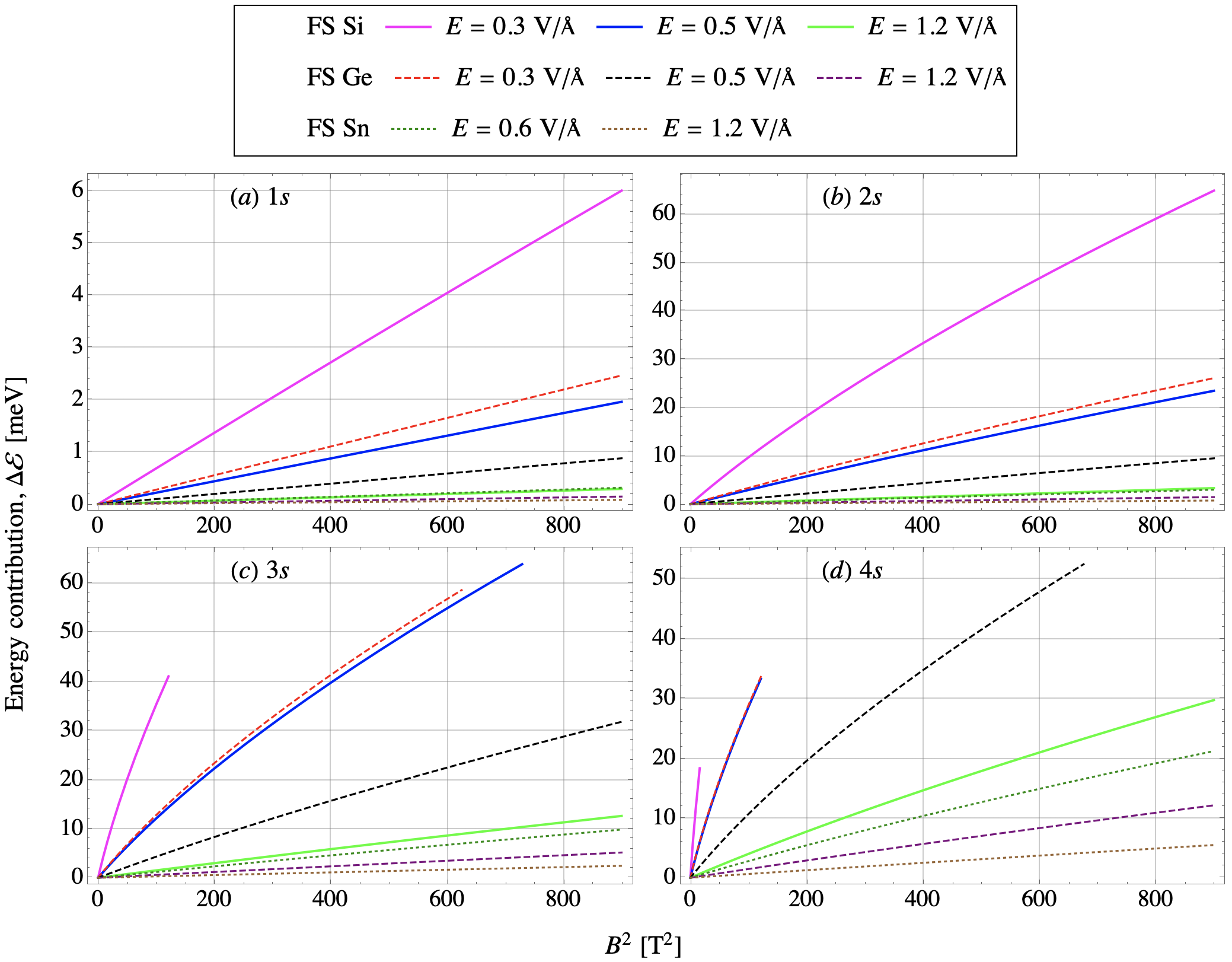
In Eq. (19) is the binding energy of the exciton in the absence of the electric and magnetic fields, while is the binding energy of the magnetoexciton at some values of the external electric and magnetic fields. The results of our calculations of energy contribution, , for direct magnetoexcitons in freestanding Xenes monolayers are reported in Fig. 3. In Figs. 3 and 3 that correspond to states 3 and 4, the end of broken curves indication dissociation of magnetoexcitons in these states. According to Fig. 3, the energy contribution from the electric and magnetic fields to the binding energy goes from the highest to the smallest in the following order: FS Si, FS Ge, FS Sn. The energy contribution due to the varying electric and magnetic fields is negligible for magnetoexcitons in FS Sn in states 1, 2, and 3 and only affects the 4 state. is significant for FS Si and FS Ge in 1, 2, 3 and 4 states when the electric field V/Å and magnetic field T; for the states 3 and 4 the contribution from both electric and magnetic fields to the binding energies of magnetoexcitons almost doubles when V/Å and T. When T, the dependence of on the electric field is very small for all states of the FS Si, FS Ge, and FS Sn. Therefore, the best range for the tunability of the energy contributions induced by the electric and magnetic fields for FS Si and Ge are V/Å (corresponds to the small reduced mass of excitons) and T.
| (a) 1 | (b) 2 |
|
 |
| (c) 3 | (d) 4 |
 |
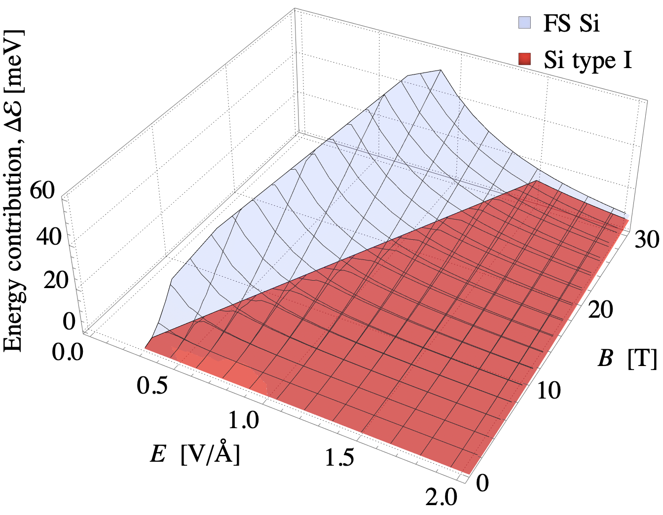 |
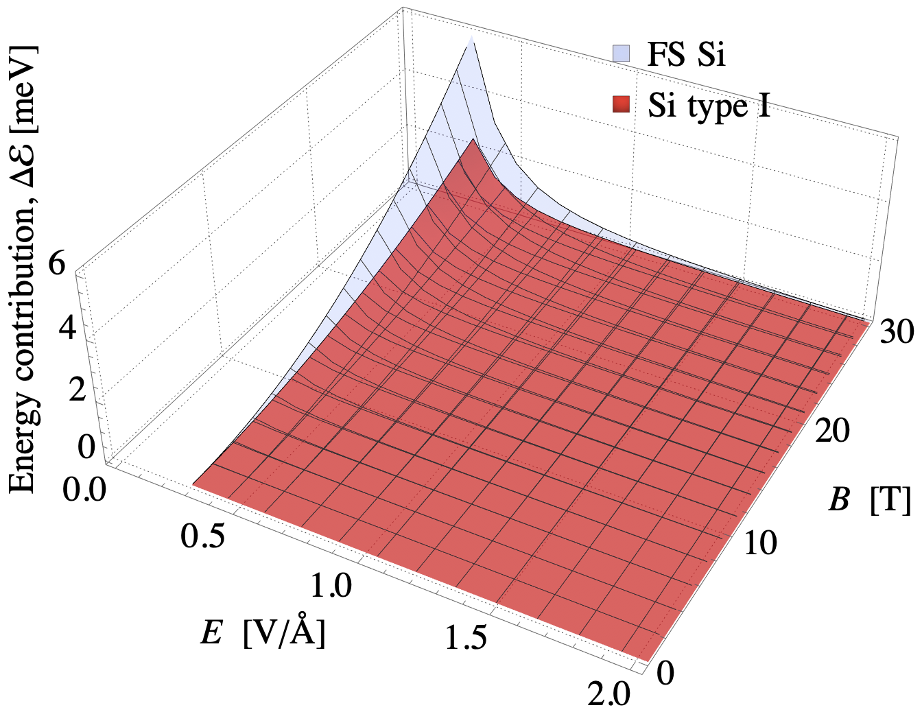
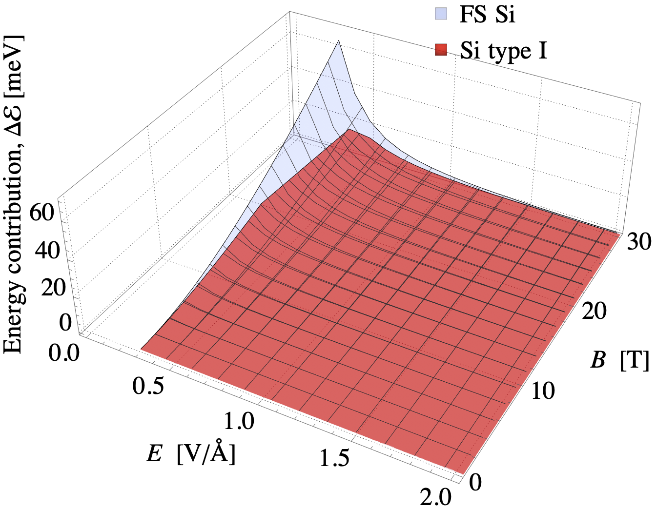
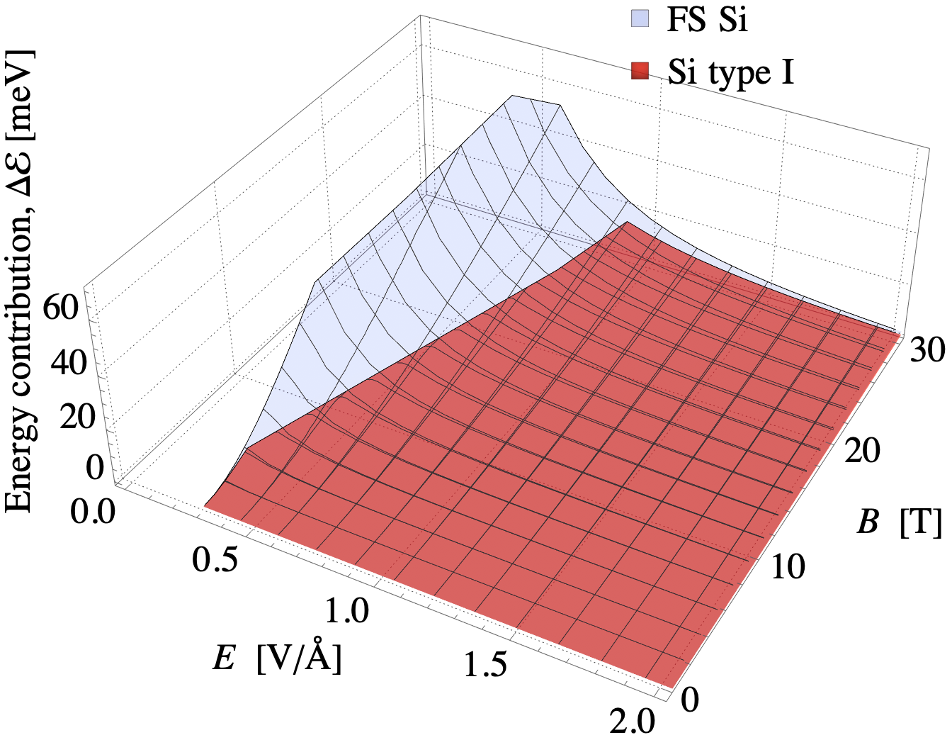
Let us now compare the dependence of the energy contribution to the binding energy of direct magnetoexcitons on the electric and magnetic fields in a freestanding silicene and encapsulated Si type I. The results of calculations for 1, 2, 3, and 4 states are presented in Fig. 4. The direct magnetoexciton in freestanding Si monolayer has a smaller effective mass, , than the magnetoexciton in silicene monolayers encapsulated by hBN. Also, the magnetoexciton in FS Si has the binding energy that is at least four times bigger than binding energies of magnetoexcitons in Si type I. As a result, magnetoexcitons in Si type monolayer at low values of dissociate at small values of the magnetic field, while magnetoexcitons in FS Si monolayers stay bound. It is worth mentioning that there are negligible differences in for direct magnetoexcitons in encapsulated Si type I and Si type II for all values of the external electric and magnetic fields, which is not shown in Fig. 4. In addition, the energy contribution for magnetoexcitons in FS Si is always larger when the electric field V/Å and T for the 1 and 2 states. The magnetoexcitons become unbound in 3 and 4 states in encapsulated Si type I monolayer with the increase of the magnetic field even for very small values of the electric field. Therefore, the difference between encapsulated and FS materials are due to substrate that gives different electron-hole masses which leads to different binding energies and energy contributions from the electric and magnetic fields to the binding energies of magnetoexcitons, especially for the 3 and 4 states. In addition, we note that magnetoexcitons in FS Ge and Si type I monolayers have similar contributions from the electric and magnetic fields to the binding energy when magnetoexcitons are bound. However, since magnetoexcitons in FS Ge monolayers have higher binding energies, magnetoexcitons in FS Ge stay bound while magnetoexcitons in Si type I monolayer in states 3 and 4 at the magnetic field values we examine. This is a notable result that indicates that the contribution from the magnetic field to the binding energy of the magnetoexciton does not only depend on the effective mass, , of electron and hole, but on material other parameters as well. The same kind of the picture can be observed if one compares the FS Ge and encapsulated Si type I and Si type II.
A careful examination of Table 1 indicates that there are different values of the Fermi velocity reported in literature Matthesparam ; Matthes2013 ; Liu2011 for FS silicene, germanene and stanene. We examined how Fermi velocity affects and the contribution from the electric and magnetic fields to the binding energy of the states 1, 2, 3, and 4. We found effective mass of magnetoexcitons in FS Si monolayer using m/s Matthesparam and m/s Matthes2013 and calculated the binding energies of the magnetoexciton. We examine the dependence of the binding energy on . Since it appears in the denominator and is squared, changing leads to the higher energy change. By calculating effective mass with different values of the band gap, the change in effective mass is smaller, and, therefore, the change in the binding energy is also smaller. Using a smaller value of leads to a higher mass since appears in the denominator in Eq. (4). As expected, results with a higher have a higher energy contribution. While the difference between two data sets is relatively small in the state 1, in the states 2, 3, and 4 the difference between two data sets is significant. This indicates two things. First, the exciton mass in Xenes is sensitive to the parameters of the material. Second, keeping all parameters the same except for indicates that has a strong dependence on effective mass, . Therefore, we can conclude that the binding energy of the magnetoexciton strongly depends on all material parameters given in Table 1.
| (a) | (b) |
|
 |
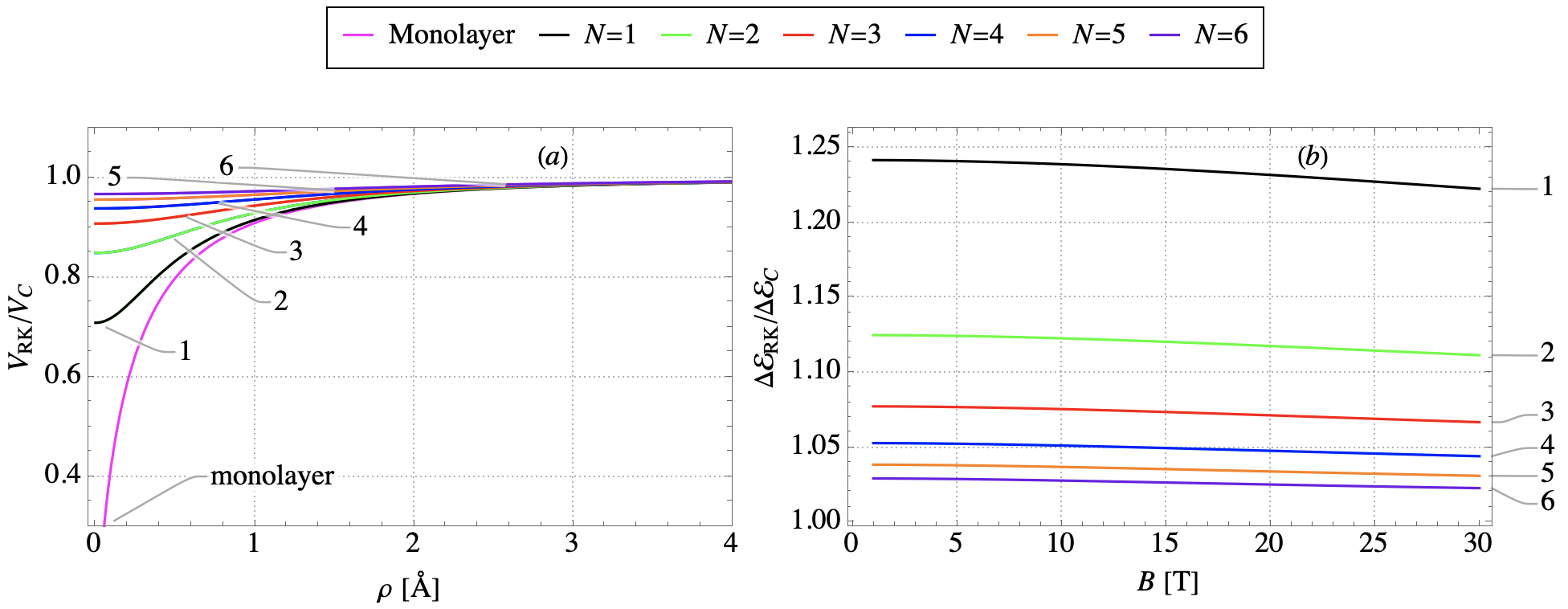
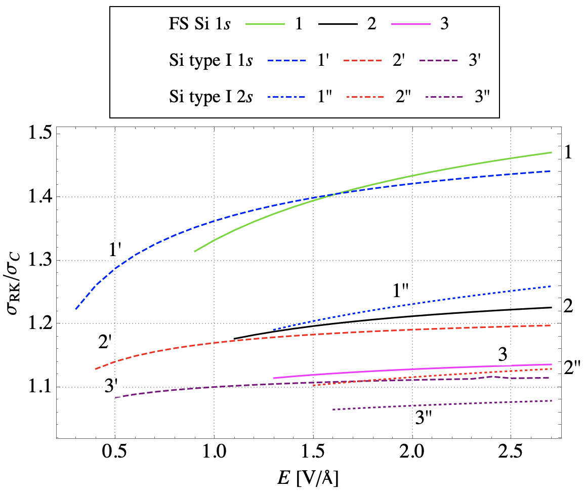
Let us now consider the energy contribution to the magnetoexcitons binding energy from the electric and magnetic fields in X-hBN-X. In a heterostructure, Xenes monolayers are separated by (=1, 2, 3, 4, 5, 6) hBN monolayers. The binding energies are calculated by using both the RK and Coulomb potentials. The latter allows to demonstrate the importance of the screening in Xenes heterostructures. A comparison of the RK and Coulomb potentials for an electron-hole pair in the Xene heterostructure Si-hBN-Si is shown in Fig. 5. On one hand, according to Fig. 5, the RK potential is weaker than the Coulomb potential at small projections, , of the electron-hole distance on the monolayer plane, and their difference significantly decreases with the increase of the number of hBN layers. On the other hand, both potentials converge to each other as and the number of hBN layers increase. From the known asymptotic properties of the Struve and Bessel functions Abramowitz ; Ryzhik , it is easy to show that . In Fig. 5, the ratio for the Si type I monolayer as a function of the electron hole separation, , is presented. In this case . The results of calculations of the ratio for the SI type I monolayer is presented in Fig. 5 and show that the Rytova-Keldysh potential gives much more contribution to the binding energies of the magnetoexciton than the Coulomb potential for all range of the magnetic field and when the number of hBN layers is less than four. As the number of hBN layers increases, the binding energies calculated with both potentials converge.
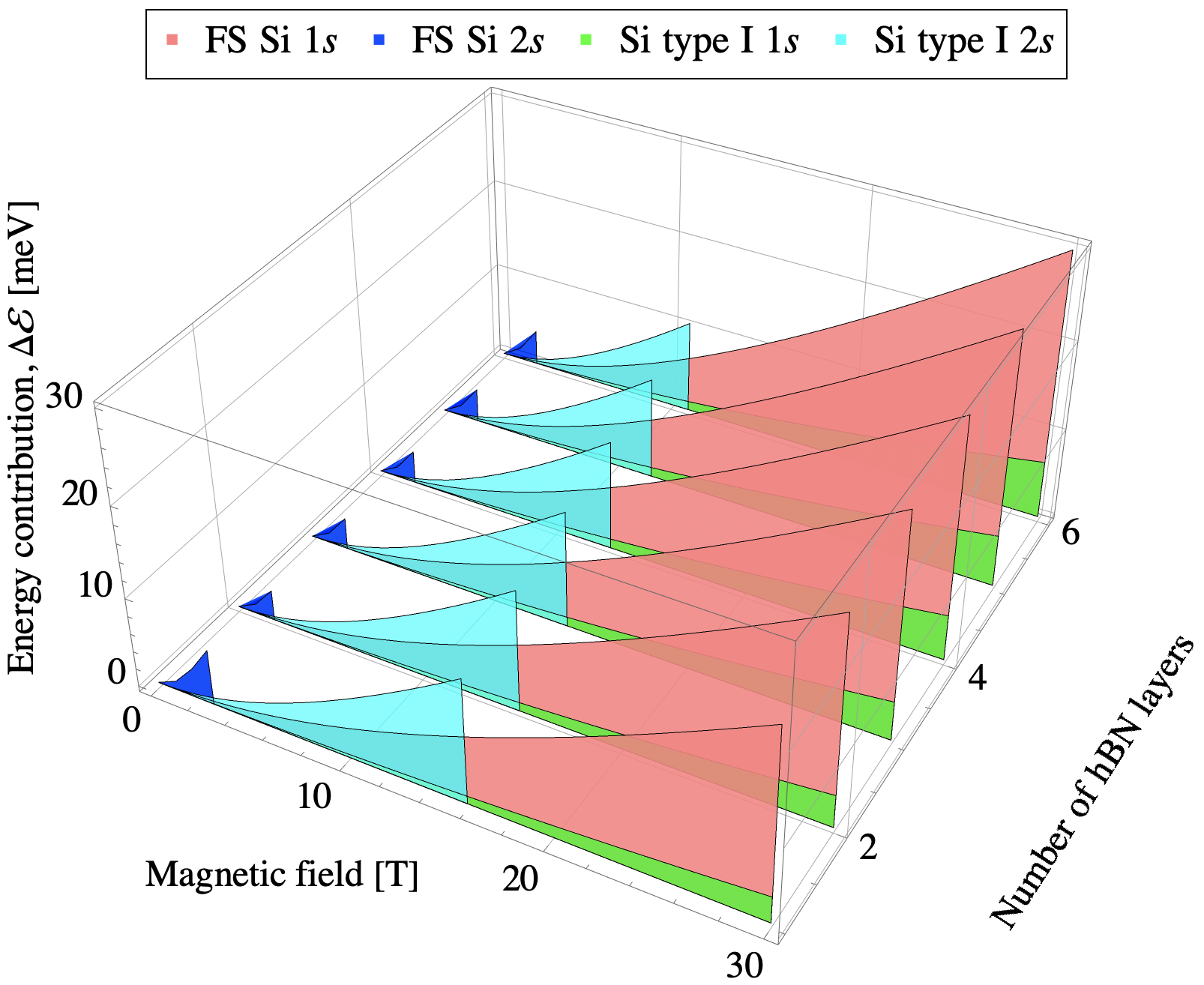
In calculations of the contribution of the electric and magnetic fields to the binding energy of magnetoexcitons in heterostructures, we focus on FS Si, Si types I and II to demonstrate the importance of using physically accurate parameters. Also, we focus on Si since there are no parameters available in literature for excitons in other encapsulated Xenes monolayers. The choice is related to the parameters of these materials listed in Table 1. From Table 1, it is clear that the parameters of FS Si differ from those for Si types I and II. We report results for indirect magnetoexcitons in Si FS and Si types I. In other words, to describe magnetoexcitons in FS Si for the direct magnetoexcitons we use parameters of FS Si with , and for indirect magnetoexcitons we use parameters of FS Si with . Therefore, we do not take into account how parameters of the FS monolayer change when it is deposited on hBN. We did so to demonstrate the importance of using physically accurate parameters of materials since it affects the binding energies. The results for indirect magnetoexcitons in the states 1 and 2 in FS Si and Si type I are reported in Fig. 6. The calculations are performed for V/Å using the RK and Coulomb potentials. In contrast to direct magnetoexcitons, in the heterostructure indirect magnetoexcitons in Si types I and II have higher binding energies than magnetoexcitons in FS Si. However, indirect magnetoexcitons in FS Si have a much higher energy contribution from the magnetic field. In overall, we have demonstrated that the energy contribution of magnetoexcitons in the monolayer and the double-layer heterostructure can be tuned by electric and magnetic fields.
In our discussion, we examine excitons because they have higher binding energies due to larger reduced masses. The results for excitons are very close to the results of excitons because above V/Å there is a small difference between the masses of and excitons in the materials we examined. The energy contribution to the binding energies of excitons is bigger for the smaller reduced mass of excitons. Because excitons have bigger reduced mass, one can consider the results of our calculations as the lower limit for the energy contribution. When two Xenes monolayers separated by hBN layers are brought together the conduction band minimum and the valence band maximum reside in two different layers forming indirect (interlayer) exciton. There are possible different stacking orders: AA and AB as in TMDCs (Pflugradt2014, ; Yarmohammad2017, ; Zhang2020, ; Schneider2019, ). The exciton, for which mass is defined by large gap, has the bigger effective masses, , of the electron and hole than the exciton formed by electron and holes with masses : . Thus, the reduced mass of excitons is bigger than the reduced mass of excitons: . In case of AA stacking, the bright interlayer exciton is formed by the hole from the valence band in valley of Layer 1 and the electron from the conduction band in valley of Layer 2 Zhang2020 . So masses of the electron and hole are equal. In case of AB stacking, because the lower layer is 180∘ in plane rotation of the upper layer Jones2014 , band spins of valley of Layer 2 are flipped compared to corresponding band spins of valley of Layer 1. As a result, the bright interlayer exciton can be formed by the hole with in valley of the Layer 1 and the electron in valley of the Layer 2 with mass (Arora2017, ; Horng2018, ; Gerber2019, ; Lorchat2021, ). This interlayer exciton has the reduced mass . Thus, . So, when the electron and hole reside in separate layers and have different masses, the binding energy of this interlayer valleys exciton falls between binding energies of interlayer excitons formed by electron and hole with equal masses. Because the energy contribution due to the magnetic field is smaller for the bigger reduced mass, our calculations for magnetoexcitons provide the lower limit for . Therefore, results for direct and indirect magnetoexcitons and indirect magnetoexcitons with the reduced mass always give higher . In our approach, the results of calculations for are only affected by the numerical value of the reduced mass, but all qualitative conclusions remain the same for all types of magnetoexcitons.
III.2
Diamagnetic shifts
The application of external electric or magnetic fields can give valuable information about the exciton. In particular, an external magnetic field has two effects on the spectroscopically observed energy levels: the spin splitting of levels, which is linear with respect to the applied field, and the diamagnetic shift - an increase in energy of levels with the magnetic field. The diamagnetic shift of an exciton in 2D materials has been studied by many of authors (DonckDM2018, ; Liu2019, ; Stier_2016, ; Aivazian, ; Gor2019, ; Macneill, ; Plechinger, ; Stier2018, ; Luckert, ; donckexc, ; Choi2015, ; Walck, ; Han2018, ; Zipfel, ; Spiridonova, ). So far diamagnetic shifts have not been considered in Xenes monolayers or double-layer heterostructures. It is our goal to extend this work to Xenes. In this paper, we apply the analysis used to describe diamagnetic shifts in quantum dots and TMDCs. Here we present the framework for Zeeman and diamagnetic shifts for magnetoexcitons in Xene monolayers and double-layer heterostructures. According to Ref. Walck , when the contribution to the binding energy from the magnetic field is small compared to the binding energy, the magnetoexciton binding energy, , for and excitons can be expanded in Taylor series as:
| (20) |
In Eq. (20) the terms and are identified as the valley Zeeman and diamagnetic shifts, respectively. The expansion of in terms of for the magnetoexciton energy given in Eq. (20) is applicable when . This expansion is no longer applicable, when , and needs the consideration of the next terms in the Taylor series. The valley Zeeman shift contribution to the binding energy is identified as , where and are -factor and Bohr magneton, respectively Aivazian ; Macneill . In Refs. Liu2019 ; Stier2018 ; Stier_2016 ; Gor2019 ; Plechinger the valley Zeeman shift for the magnetoexciton in the monolayer is defined as the energy difference between magnetoexcitons located at Dirac points and , Liu2019 ; Stier2018 ; Stier_2016 ; Gor2019 ; Plechinger . The diamagnetic shift contribution to the binding energy is identified as Stier2018 ; Stier_2016 , where is the exciton reduced mass, is the charge of the electron, and is the expectation value of over the exciton envelope wave function. The factor is called the diamagnetic coefficient, and we denote it as . In the case of Xenes the reduced mass is and the diamagnetic shift contribution to the binding energy is . Experimentally the energy contribution from the diamagnetic shift is defined as the average transition energy of each magnetoexciton state between points and , Liu2019 ; Stier2018 ; Stier_2016 ; Chen2019 ; Macneill . In TMDCs DMCs are used to determine exciton masses, radius, and dielectric properties of materials. For similar purposes, can be used for excitons in Xene monolayers.
We have calculated the diamagnetic coefficients for magnetoexcitons in monolayers of FS Si, FS Ge, FS Sn, Si types I and II for the Rydberg states, 1, 2, 3, and 4. The DMCs for the direct magnetoexcitons in the above materials are reported in Fig. 7. The plotted data takes into account the critical value of below which the material behaves like excitonic insulator (Knox, ; BBKPRB2019, ). In Fig. 7 at the bottom and the top of each graph scales for the electric field, , and the corresponding effective mass, , respectively, are given. In contrast to for magnetoexcitons in TMDCs monolayers reported only for 1 and 2 states in Ref. Spiridonova , for magnetoexcitons in Xene monolayers can be calculated for states 1, 2, 3, and 4. At smaller values of the external electric field , the dependence of on is not linear for magnetoexcotons in states 2s, 3s, and 4s. For direct magnetoexcitons at smaller values of higher order terms in Taylor expansion, Eq. (20), need to be considered. As can be seen from Fig. 7, in the states 2, 3, and 4 magnetoexcitons have diamagnetic shifts at electric field V/Å, while the magnetoexciton in FS Sn has for all states when .
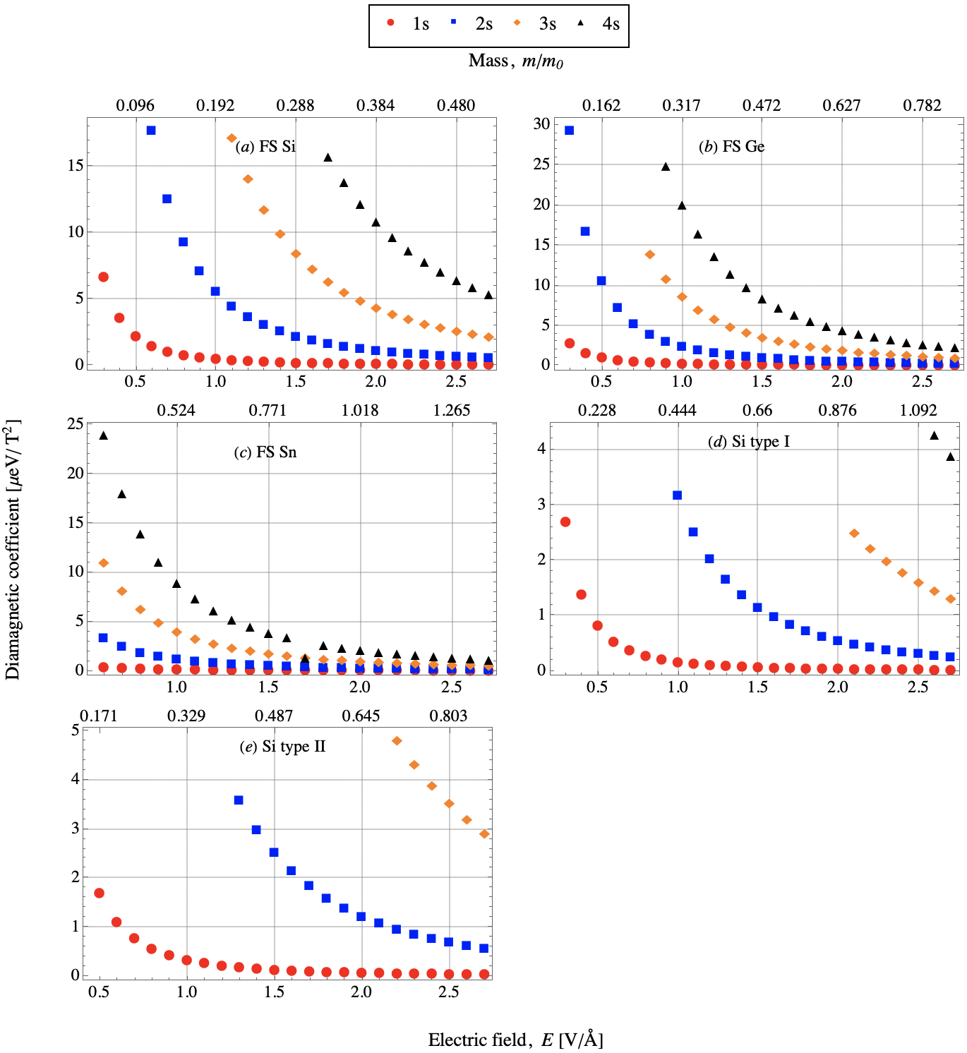
As can be seen from Figs. 7 and 7, at the smaller value of in FS Si and FS Ge, respectively, parameters give lower reduced mass which leads to higher energy contribution and higher DMCs. According to Fig. 7, as increases the DMCs of direct magnetoexcitons in the examined states and materials decrease and approach 0. The condition exists for magnetoexcitons in some materials at low values of in states 2, 3, and 4, and we cannot apply Eq. (20) to extract from our data. The condition is prominent in Si types I and II monolayers because magnetoexcitons in Si types I and II monolayers in states 2, 3, and 4 have the binding energies four times smaller than excitons in corresponding states in monolayers of FS materials. Also as it can be seen from Fig. 7, the magnetoexcitons in Si type II in the state 4 has no diamagnetic shift. Note, that magnetoexcitons in Si types I and II monolayers and double-layer heterostructures have the same energy contribution to the binding energy and DMCs at the same values of . However, the magnetoexcitons in Si types I and II have different critical values of and have different values of at the same value of . On one hand, direct magnetoexcitons in Si types I and II monolayers at small values of quickly dissociate when the perpendicular magnetic field is applied to the monolayer. For example, the magnetoexciton in Si type I (type II) at V/Å in state 3 dissociates at 11 T (7 T) and in state 4 at 5 T (3 T). On the other hand, direct magnetoexcitons in monolayers of the FS Xenes in states 2, 3, and 4 stay bound at higher values of the magnetic field and satisfy the condition, , even at small values of electric field, , that correspond to the small mass and allow us to extract DMCs.
| (a) 1 | (b) 1 |
|
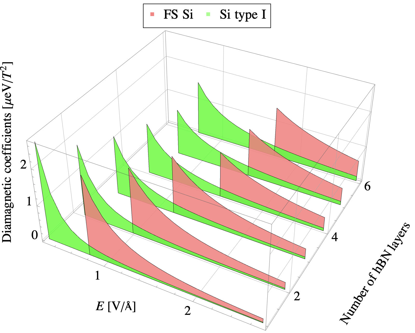 |
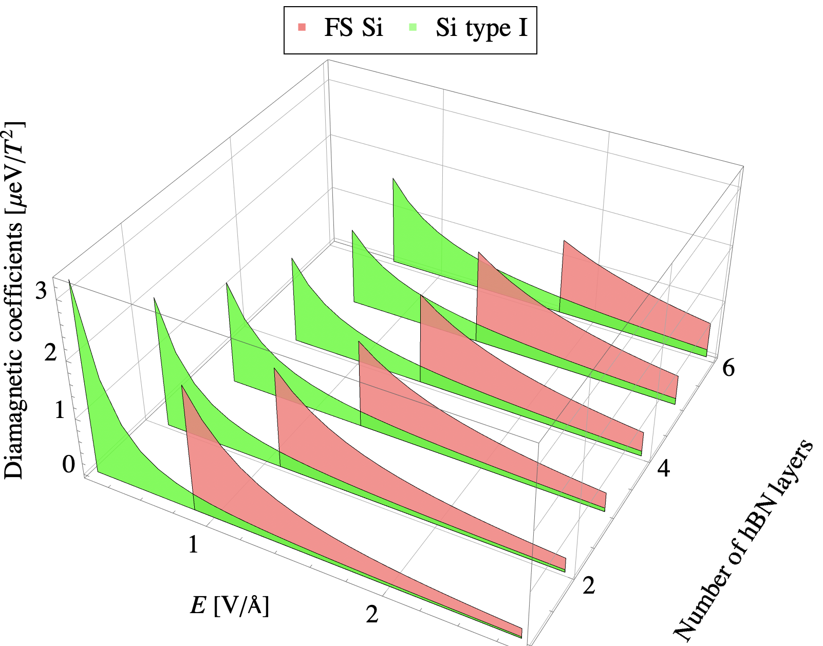
For indirect magnetoexcitons in the double-layer heterostructure from the calculated binding energies with both the Rytova-Keldysh and Coulomb potentials, we extracted the DMCs of the magnetoexcitons for FS silicene and Si type I. The results for DMCs of indirect magnetoexcitons in the double-layer heterostructure of Xenes are shown in Fig. 8. The comparison of DMCs calculated from binding energies obtained with the RK and Coulomb potentials is shown only for indirect magnetoexcitons in FS Si and Si type I. Our calculations show that magnetoexcitons in other Xenes double-layer heterostructures have similar quantitative and qualitaive behavior. As the electric field increases (the corresponding effective masse of the electron and holes increases) and the number of hBN layers increases the DMCs decrease and approach zero. The DMCs for indirect magnetoexcitons calculated with and potentials converge with the increase of the electric field, as can be seen from Fig. 8. However, the DMCs obtained by using the RK potential are higher. Therefore, the choice of interaction potential is important when a few hBN layers separate the Xene monolayers. Another important effect of the number of hBN layers is that as the distance between Xene monolayers increases the energy contribution from the magnetic field to the binding energy does not have linear dependence on . More specifically, as the distance between Xene monolayers increases the lowest value of at which linear dependence of on exists increases.
We also analyze the dependence of the ratio /, where and are diamagnetic coefficients of indirect magnetoexcitons obtained using the RK and Coulomb potentials, respectively, on the external electric field and number of hBN layers. The corresponding results are presented in Fig. 9 for the indirect magnetoexcitons in FS Si for the state 1 and Si type I for states 1 and 2. For the magnetoexcitons in FS Si in state 2, there is no linear dependence of on , and the ratio is not presented. When the external electric field V/Å, the DMCs for FS Si and Si type I are close and have the same qualitative dependence on and number of hBN layers. As a result, we can conclude that the diamagnetic coefficients can be tuned by the external electric field as well as by changing interlayer separation by changing the number of hBN layers.
IV Conclusion
We study Rydberg states of direct and indirect magnetoexcitons in monolayers and double-layer heterostructures of Xenes in the presence of the external perpendicular to the layer electric and magnetic fields. We consider the freestanding silicene, germanene, and stanene monolayers and Si type I and II encapsulated by hBN monolayers and Xenes heterostructures. We have calculated the binding energies, the energy contribution from the electric and magnetic fields to the binding energy, and diamagnetic coefficients for magnetoexcitons in monolayer and heterostructure of Xenes. We solve the Schrödinger equation with the magnetoexciton reduced mass dependent on the perpendicular electric field by numerical integration to obtain eigenvalues and eigenfunctions. For the direct magnetoexcitons, the Schrödinger equation is solved using the Rytova-Kyldysh potential, and for the indirect excitons, the Schrödinger equation is solved with both the RK and Coulomb potentials.
The contribution from the electric and magnetic fields to the binding energy of the magnetoexcitons in Rydberg states, 1, 2, 3, and 4, for freestanding and encapsulated monolayers as a function of the external perpendicular electric and magnetic fields is analyzed. The analysis of DMCs for magnetoexcitons in above mentioned systems and their dependence on the external electric field and number of hBN layers are presented as well. Only in monolayer magnetoexcitons had linear dependence of energy contributions on in states 1, 2, 3, and 4. The linear dependence of on is not present for indirect magnetoexcitons in all states. The DMCs for the states 1, 2, 3 and 4 can be calculated only for direct magnetoexcitons in FS Si, FS Ge, FS Sn and Si type I. For indirect magnetoexcitons, DMCs can be calculated for states 1 and 2. As the number of layers that separate Xenes monolayers increases, the binding energies of Rydberg states decrease, and energy contribution from the electric and magnetic fields to the binding energy for given values of the electric field no longer has a linear dependence on . A smaller effective mass (small external electric field) leads to a higher energy contribution from the magnetic field to the binding energy and potentially higher DMCs. However, small and high energy contribution from the magnetic field to the binding energy lead to absence of linear dependence of the energy contribution on and, therefore, the DMCs cannot be extracted.
The most bound direct magnetoexcitons are found in the FS Si monolayer. The magnetoexcitons in FS Si have the smallest effective and reduced masses out of all materials that we have examined. However, the material constants of the encapsulating materials also play an important role in determining the properties of excitons in the monolayer and, therefore, the binding energy of the exciton as can be seen by examining the heterostructure. From our calculation, we can see that, by taking the magnetoexciton with parameters of FS monolayer and then the encapsulating monolayer with hBN, magnetoexcitons have smaller binding energies than magnetoexcitons in Si type I monolayer. The indirect magnetoexcitons are most bound in Si type I monolayer. So we conclude that, while the effective mass has the strong effect on the binding energy and the energy contribution from the magnetic field to the binding energy, the dielectric constants of the encapsulating materials also have a significant effect on the binding energy.
The analysis of Xenes parameters shows that Si type I has a smaller gap and Fermi velocity than Si type II, and, therefore, magnetoexcitons in Si type I monolayer have higher effective mass and binding energies than magnetoexcitons in Si type II. But the magnetoexcitons in Si type II has higher DMCs and higher energy contribution from the electric and magnetic fields to the binding energy in monolayer and heterostructure since the magnetoexciton in Si type II monolayer has smaller than the magnetoexciton in Si type I monolayer at the same value of the electric field. Thus, the importance of using physically accurate parameters of the material, since they affect the binding energies and DMCs, is shown.
The comparison of the results for Xenes heterostructure obtained by using the Rytova-Keldysh and Coulomb potentials shows that and converge as the number of layers increases. The binding energies, , and DMCs converge as the number of hBN layers increases. The energy contribution to the binding energy of the magnetoexciton calculated with is higher than the energy contribution calculated using when only a few layers separate Xenes monolayers. The diamagnetic coefficients extracted from the binding energy of the magnetoexciton calculated using are higher than when is used. However, in both cases, the DMCs converge as and the number of hBN layers increase. Therefore, the choice of the interaction potential affects the energy contribution from the electric and magnetic fields and DMCs (when the contribution is proportional to ), and it is important to use appropriate interaction potential for the system when only a few layers separate magnetoexciton containing monolayers.
Finally, we can conclude that external electric and magnetic fields can be effectively used for tuning their contribution to the binding energy of both direct and indirect magnetoexcitons in Xenes, while for the Xenes heterostructure the varying of the number of hBN separating layers provides the additional degree of freedom to tune the binding energy of indirect magnetoexcitons. The tunability of the diamagnetic coefficients by the external electric field for both direct and indirect magnetoexcitons and by the change of the number of hBN separated Xenes layers for indirect magnetoexcitons is also demonstrated. Thus, the tunability of direct and indirect magnetoexcitons properties allows the design of electronic devices that can be manipulated by the external electric and magnetic fields and the number of hBN separating Xenes layers in heterostructure.
Acknowledgments. This work is supported by the U.S. Department of Defense under Gran No. W911NF1810433 and PSC-CUNY Award No. 62261-00 50.
References
- (1) K. S. Novoselov, A. K. Geim, S. V. Morozov, D. Jiang, Y. Zhang, S. V. Dubonos, I. V. Grigorieva, and A. A. Firsov, Electric Field Effect in Atomically Thin Carbon Films, Science , 666 (2004).
- (2) S. J. McDonnell and R. M. Wallace, Atomically-Thin Layered Films for Device Applications Based upon 2D TMDC Materials, Solid Films , 482 (2016).
- (3) K. S. Novoselov, A. Mishchenko, A. Carvalho, and A. H. Castro Neto, 2D materials and van der Waals heterostructures, Science , (2016).
- (4) S. Heerema and C. Dekker, Graphene nanodevices for DNA sequencing, Nature. Nanotech. , 127–136 (2016).
- (5) G. Iannaccone, F. Bonaccorso, L. Colombo, and G. Fiori, Quantum engineering of transistors based on 2D materials heterostructures, Nature. Nanotech. , 183–191 (2018).
- (6) A. H. Castro Neto, F. Guinea, N. M. R. Peres, K. S. Novoselov, and A. K. Geim, The electronic properties of graphene, Rev. Mod. Phys. , 109 (2009).
- (7) P. Avouris, T. Heinz, and T. Low (Eds.). (2017). 2D Materials: Properties and Devices. Cambridge: Cambridge University Press, 2017. doi:10.1017/9781316681619.
- (8) J. Zheng, Y. Xiang, C. Li, R. Yuan, F. Chi, and Y. Guo, All-Optically Controlled Topological Transistor Based on enes, Phys. Rev. Applied , 034027 (2020).
- (9) A. Molle, J. Goldberger, M. Houssa, Y. Xu, S. C. Zhang, and D. Akinwande, Buckled two-dimensional Xene sheets, Nat. Mater. , 163(2017).
- (10) C. Grazianetti, C. Martella, and A. Molle, The Xenes Generations: A Taxonomy of Epitaxial Single‐Element 2D Materials, Phys. Status Solidi RRL , 1900439 (2020).
- (11) L. Matthes, O. Pulci, and F. Bechstedt, Massive Dirac quasiparticles in the optical absorbance of graphene, silicene, germanene, and tinene, J. Phys.: Condens. Matter , 395305 (2013).
- (12) Y. Li, J. Ludwig, T. Low, A. Chernikov, X. Cui, G. Arefe, Y. D. Kim, A. M. van der Zande, A. Rigosi, H. M. Hill, S. H. Kim, J. Hone, Z. Li, D. Smirnov, and T. F. Heinz, Valley Splitting and Polarization by the Zeeman Effect in Monolayer MoSe2, Phys. Rev. Lett. , 266804 (2014).
- (13) D. MacNeill, C. Heikes, K. F. Mak, Z. Anderson, A. Kormányos, V. Zólyomi, J. Park, and D. C. Ralph, Breaking of Valley Degeneracy by Magnetic Field in Monolayer MoSe2, Phys. Rev. Lett. , 037401 (2015).
- (14) A. Srivastava, M. Sidler, A. Allain, D. S. Lembke, A. Kis and A. Imamoğlu, Valley Zeeman effect in elementary optical excitations of monolayer WSe2, Nat. Phys. , 141 (2015).
- (15) G. Aivazian, Z. Gong, A. Jones, R. L. Chu, J. Yan, D. G. Mandrus, C. Zhang, D. Cobden, W. Yao, and X. Xu, Magnetic control of valley pseudospin in monolayer WSe2, Nat. Phys. , 148 (2015).
- (16) M. Z. Mayers, T. C. Berkelbach, M. S. Hybertsen, and D. R. Reichman, Binding energies and spatial structures of small carrier complexes in monolayer transition-metal dichalcogenides via diffusion Monte Carlo, Phys. Rev. B , 161404(R) (2015).
- (17) D. W. Kidd, D. K. Zhang, and K. Varga, Binding energies and structures of two-dimensional excitonic complexes in transition metal dichalcogenides, Phys. Rev. B , 125423 (2016).
- (18) G. Plechinger, P. Nagler, A. Arora, A. G. del Águila, M. V. Ballottin, T. Frank, P. Steinleitner, M. Gmitra, J. Fabian, P. C. M. Christianen, R. Bratschitsch, C. Schuller, and T. Korn, Excitonic Valley Effects in Monolayer WS2 under High Magnetic Fields, Nano Lett. , 7899 (2016).
- (19) A. Stier, K. McCreary, B. Jonker, J. Kono, and S. A. Crooker, Exciton diamagnetic shifts and valley Zeeman effects in monolayer WS2 and MoS2 to 65 Tesla, Nat. Commun. , 10643 (2016).
- (20) C. Robert, M. A. Semina, F. Cadiz, M. Manca, E. Courtade, T. Taniguchi, K. Watanabe, H. Cai, S. Tongay, B. Lassagne, P. Renucci, T. Amand, X. Marie, M. M. Glazov, and B. Urbaszek, Optical spectroscopy of excited exciton states in MoS2 monolayers in van der Waals heterostructures, Phys. Rev. Materials , 011001(R) (2018).
- (21) J. Zipfel, J. Holler, A. A. Mitioglu, M. V. Ballottin, P. Nagler, A. V. Stier, T. Taniguchi, K. Watanabe, S. A. Crooker, P. C. M. Christianen, T. Korn, and A. Chernikov, Spatial extent of the excited exciton states in WS2 monolayers from diamagnetic shifts, Phys. Rev. B , 075438 (2018).
- (22) E. Liu, J. Baren, T. Taniguchi, K. Watanabe, Y. C. Chang, and C. H. Lui, Magnetophotoluminescence of exciton Rydberg states in monolayer WSe2, Phys. Rev. B , 205420 (2019).
- (23) A. Arora, T. Deilmann, T. Reichenauer, J. Kern, S. M. de Vasconcellos, M. Rohlfing, and R. Bratschitsch, Excited-State Trions in Monolayer WSe2, Phys. Rev. Lett. , 167401 (2019).
- (24) M. Koperski, M. R. Molas, A. Arora, K. Nogajewski, M. Bartos, J. Wyzula, D. Vaclavkova, P. Kossacki, and M. Potemski, Orbital, spin and valley contributions to Zeeman splitting of excitonic resonances in MoSe2, WSe and WS2 Monolayers, 2D Mater. , 015001 (2019).
- (25) S. Y. Chen, Z. Lu, T. Goldstein, J. Tong, A. Chaves, J. Kunstmann, L. S. R. Cavalcante, T. Woźniak, G. Seifert, D. R. Reichman, T. Taniguchi, K. Watanabe, D. Smirnov, and J. Yan, Luminescent Emission of Excited Rydberg Excitons from Monolayer WSe2, Nano Lett. , 2464 (2019).
- (26) M. Goryca, J. Li, A. V. Stier, T. Taniguchi, K. Watanabe, E. Courtade, S. Schree, C. Robert, B. Urbaszek, X. Maria, and S. A. Crooker, Revealing exciton masses and dielectric properties of monolayer semiconductors with high magnetic fields, Nat. Commun. , 4172 (2019).
- (27) T. Goldstein, Y. C. Wu, S. Y. Chen, T. Taniguchi, K. Watanabe, K. Varga, and J. Yan, Ground and Excited Exciton Polarons in Monolayer MoSe2, J. Chem. Phys. , 071101 (2020).
- (28) E. Liu, J. Baren, Z. Lu, T. Taniguchi, K. Watanabe, D. Smirnov, Y. C. Chang, and C. H. Lui, Gate-tunable exciton-polaron Rydberg series with strong roton effect, (arXiv:2006.04895).
- (29) D. V. Rybkovskiy, I. C. Gerber, and M. V. Durnev, Atomically inspired approach and valley Zeeman effect in transition metal dichalcogenide monolayers, Phys. Rev. B , 155406 (2017).
- (30) M. Van der Donck, M. Zarenia, and F. M. Peeters, Strong valley Zeeman effect of dark excitons in monolayer transition metal dichalcogenides in a tilted magnetic field, Phys. Rev. B , 081109(R) (2018).
- (31) S. N. Walck and T. L. Reinecke, Exciton diamagnetic shift in semiconductor nanostructures, Phys. Rev. B , 9088 (1998).
- (32) F. Luckert, M. V. Yakushev, C. Faugeras, A. V. Karotki, A. V. Mudryi, and R. W. Martin, Diamagnetic shift of the A free exciton in CuGaSe2 single crystals, Appl. Phys. Lett. , 162101 (2010).
- (33) B. K. Choi, Y. Kim, and J. D. Song, Diamagnetic Shift of a InGaP-AlInGaP Semiconductor Single Quantum Well under Pulsed-magnetic Fields, Applied Science and Convergence Technology , 156 (2015).
- (34) M. Van der Donck, M. Zarenia, and F. M. Peeters, Excitons, trions, and biexcitons in transition-metal dichalcogenides: Magnetic-field dependence, Phys. Rev. B , 195408 (2018).
- (35) A. V. Stier, N. P. Wilson, K. A. Velizhanin, J. Kono, X. Xu, and S. A. Crooker, Magnetooptics of Exciton Rydberg States in a Monolayer Semiconductor, Phys. Rev. Lett. , 057405 (2018).
- (36) B. Han, C. Robert, E. Courtade, M. Manca, S. Shree, T. Amand, P. Renucci, T. Taniguchi, K. Watanabe, X. Marie, L. E. Golub, M. M. Glazov, and B. Urbaszek, Exciton States in Monolayer MoSe2 and MoTe2 Probed by Upconversion Spectroscopy, Phys. Rev. X , 031073 (2018).
- (37) A. Spiridonova, Magnetoexcitons in monolayer transition-metal dichalcogenides, Phys. Lett. A , 126850 (2020).
- (38) L. Tao, E. Cinquanta, D. Chiappe, C. Grazianetti, M. Fanciulli, M. Dubey, A. Molle, and D. Akinwande, Silicene field-effect transistors operating at room temperature, Nat. Nanotechnol. , 227 (2015).
- (39) B. Aufray, A. Kara, S. Vizzini, H. Oughaddou, C. Léandri, B. Ealet, and G. L. Lay, Graphene-like silicon nanoribbons on Ag(110): A possible formation of silicene, Appl. Phys. Lett. , 183102 (2010).
- (40) P. E. Padova, C. Quaresima, C. Ottaviani, P. M. Sheverdyaeva, P. Moras, C. Carbone, D. Topwal, B. Olivieri, A. Kara, H. Oughaddou, B. Aufray, and G. L. Lay, Evidence of graphene-like electronic signature in silicene nanoribbons, Appl. Phys. Lett. , 261905 (2010).
- (41) N. D. Drummond, V. Zólyomi, and V. I. Fal’ko, Electrically tunable band gap in silicene, Phys. Rev. B 85, 075423 (2012).
- (42) M. E. Dávila, L. Xian, S. Cahangirov, A. Rubio, and G. L. Lay, Germanene: a novel two-dimensional germanium allotrope akin to graphene and silicene, New J. Phys , 095002 (2014).
- (43) S. Saxena, R. P. Chaudhary, and S. Shukla, Stanene: Atomically Thick Free-standing Layer of 2D Hexagonal Tin, Sci. Rep. , 31073 (2016).
- (44) A. J. Mannix, B. Kiraly, M. C. Hersam, and N. P. Guisinger, Synthesis and chemistry of elemental 2D materials, Nat. Rev. Chem. , 0014 (2017).
- (45) D. D. Sante, X. Wu, M. Fink, W. Hanke, and R. Thomale, Triplet superconductivity in the Dirac semimetal germanene on a substrate, Phys. Rev. B , 201106(R) (2019).
- (46) L. Li, X. Wang, X. Zhao, and M. Zhao, Moiré superstructures of silicene on hexagonal boron nitride: A first-principles study Author links open overlay panel, Phys. Lett. A , 2628 (2013).
- (47) A.I. Khan, T. Chakraborty, N. Acharjee, and S. Subrina, Stanene-hexagonal boron nitride heterobilayer: Structure and characterization of electronic property, Sci. Rep. , 16347 (2017).
- (48) M. Ezawa, Quantum Hall Effects in Silicene, J. Phys. Soc. Jpn. , 064705 (2012).
- (49) J. Zhao, H. Liu, Z. Yu, R. Quhe, S. Zhou, Y. Wang, C. C. Liu, H. Zhong, N. Han, J. Lu, Y. Yao, and K. Wu, Rise of silicene: A competitive 2D material, Prog. Mater. Sci. , 24 (2016).
- (50) F. Bechstedt, L. Matthes, P. Gori, and O. Pulci, Infrared absorbance of silicene and germanene, Appl. Phys. Lett. , 261906 (2012).
- (51) M. Fadaie, N. Shahtahmassebi, and M. R. Roknabad, Effect of external electric field on the electronic structure and optical properties of stanene, Opt. Quantum Electron. , 440 (2016).
- (52) L. Stille, C. J. Tabert, and E. J. Nicol, Optical signatures of the tunable band gap and valley-spin coupling in silicene, Phys. Rev. B , 195405 (2012).
- (53) D. Muoi, N. N. Hieu, and C. V. Nguyen, Magneto-optical absorption in silicene and germanene induced by electric and Zeeman fields, Phys. Rev. B , 205408 (2020).
- (54) S. Chowdhury and D. Jana, A theoretical review on electronic, magnetic and optical properties of silicene, Rep. Prog. Phys. , 126501 (2016).
- (55) X. Zhai, Y. T. Wang, R. Wen, S. X. Wang, Y. Tian, X. Zhou, W. Chen, and Z. Yang, Valley-locked thermospin effect in silicene and germanene with asymmetric magnetic field induced by ferromagnetic proximity effect, Phys. Rev. B , 085410 (2018).
- (56) M. Ezawa, Valley-Polarized Metals and Quantum Anomalous Hall Effect in Silicene, Phys. Rev. Lett. , 055502 (2012).
- (57) A. Zhao and B. Wang, Two-dimensional graphene-like Xenes as potential topological materials, APL Materials , 030701 (2020).
- (58) C. H. Chen, W. W. Li, Y. M. Chang, C. Y. Lin, S. H. Yang, Y. Xu, and Y. F. Lin, Negative-Differential-Resistance Devices Achieved by Band-Structure Engineering in Silicene under Periodic Potentials, Phys. Rev. Applied , 044047 (2018).
- (59) N. R. Glavin, R. Rao, V. Varshney, E. Bianco, A. Apte, A. Roy, E. Ringe, and P. M. Ajayan, Emerging Applications of Elemental 2D Materials, Adv. Mater. , 1904302 (2019).
- (60) J. Lyu, S. Zhang, C. Zhang, and P. Wang, Stanene: A Promising Material for New Electronic and Spintronic Applications, ANNALEN DER PHYSIK 2019, 531, 1900017.
- (61) C. Grazianetti, C. Martella, and A. Molle, Two-dimensional xenes and their device concepts for future micro- and nanoelectronics and energy applications. In book Emerging 2D materials and devices for the internet of things. L. Tao and D. Akinwande (Elsevier, Amsterdam, Netherlands, 2020), pp. 181-219.
- (62) V. Yu. Tsaran and S. G. Sharapov, Landau levels and magnetic oscillations in gapped Dirac materials with intrinsic Rashba interaction, Phys. Rev. B , 205417 (2014).
- (63) Yu. E. Lozovik and V. I. Yudson, A new mechanism for superconductivity: pairing between spatially separated electrons and holes, Zh. Eksp. Teor. Fiz. 71, 738 (1976) [Sov. Phys. JETP 44, 389 (1976)].
- (64) N. S. Rytova, Screened potential of a point charge in a thin film, Proc. Moscow State University, Phys. Astron. , 30 (1967).
- (65) L. V. Keldysh, Coulomb interaction in thin semiconductor and semimetal films, JETP Lett. , 658 (1979).
- (66) C. J. Tabert and E. J. Nicol, Dynamical polarization function, plasmons, and screening in silicene and other buckled honeycomb lattices, Phys. Rev. B 89, 195410 (2014).
- (67) M. Ezawa, Spin-valley optical selection rule and strong circular dichroism in silicene, Phys. Rev. B 86, 161407(R) (2012).
- (68) D. S. L. Abergel, V. Apalkov, J. Berashevich, K. Ziegler, and T. Chakraborty, Properties of graphene: a theoretical perspective, Adv. Phys. , 261 (2010).
- (69) C. L. Kane and E. J. Mele, Quantum Spin Hall Effect in Graphene, Phys. Rev. Lett. 95, 226801 (2005).
- (70) J. P. Echeverry, B. Urbaszek, T. Amand, X. Marie, and I. C. Gerber, Splitting between bright and dark excitons in transition metal dichalcogenide monolayers, Phys. Rev. B 93, 121107(R) (2016).
- (71) E. Malic, M. Selig, M. Feierabend, S. Brem, D. Christiansen, F. Wendler, A. Knorr, and G. Bergäuser, Dark excitons in transition metal dichalcogenides, Phys. Rev. Materials 2, 014002 (2018).
- (72) F. Pan, Y Wang, K. Jiang, Z. Ni, J. Ma, J. Zheng, R. Quhe, J. Shi, J. Yang, C. Chen, and J. Lu, Silicene nanomesh, Sci. Rep. , 9075 (2015).
- (73) C. C. Liu, W. Feng, and Y. Yao, Quantum Spin Hall Effect in Silicene and Two-Dimensional Germanium, Phys. Rev. Lett. , 076802 (2011).
- (74) C. C. Liu, H. Jiang, and Y. Yao, Low-energy effective Hamiltonian involving spin-orbit coupling in silicene and two-dimensional germanium and tin, Phys. Rev. B , 195430 (2011).
- (75) L. Matthes, P. Gori, O. Pulci, and F. Bechstedt, Universal infrared absorbance of two-dimensional honeycomb group-IV crystals, Phys. Rev. B 87, 035438 (2013).
- (76) R. Ya. Kezerashvili, Few-body systems in condensed matter physics, Few-Body Syst. 60, 52, (2019).
- (77) O. L. Berman, R. Ya. Kezerashvili, and K. Ziegler, Coupling of two Dirac particles, Phys. Rev. A 87, 042513 (2013).
- (78) T. C. Berkelbach, M. S. Hybertsen, and D. R. Reichman, Theory of neutral and charged excitons in monolayer transition metal dichalcogenides, Phys. Rev. B 88, 045318 (2013).
- (79) G. Wang, A. Chernikov, M. M. Glazov, T. F. Heinz, X. Marie, T. Amand, and B. Urbaszek, Colloquium: Excitons in atomically thin transition metal dichalcogenides, Rev. Mod. Phys. 90, 021001 (2018).
- (80) M. M. Fogler, L. V. Butov, and K. S. Novoselov, High-temperature superfluidity with indirect excitons in van der Waals heterostructures, Nat. Commun. 5, 4555 (2014).
- (81) O. L. Berman and R. Ya. Kezerashvili, High-temperature superfluidity of the two-component Bose gas in a transition metal dichalcogenide bilayer, Phys. Rev. B 93, 245410 (2016).
- (82) G. Wannier, The structure of electronic excitation levels in insulating crystals, Phys. Rev. , 191 (1937).
- (83) H. Herold, H. Ruder, and G. Wunner, The two-body problem in the presence of a homogeneous magnetic field, J. Phys. B: At. Mol. Phys. , 751 (1981).
- (84) R. J. Elliott and R. Loudon, Theory of the absorption edge in semiconductors in a high magnetic field, J. Phys. Chem. Solids , 196 (1960).
- (85) L. P. GorKov and I. E. Dzualoshinskii, Contribution to the theory of the Mott exciton in a strong magnetic field, Zh. Eksp. Teor. Fiz. , 717 (1967).
- (86) Yu. E. Lozovik and A. M. Ruvinsky, Magnetoexcitons in coupled quantum wells, Phys. Rev. Lett. A. , 271284 (1997).
- (87) M. Shinada and S. Sugano, Optical Absorption Edge in Layer-Type Semiconductors, J. Phys. Soc. Jpn. , 1274 (1965).
- (88) O. Akimoto and H. Hasegawa, Interband Optical Transitions in Extremely Anisotropic Semiconductors. II. Coexistence of Exciton and the Landau Levels, J. Phys. Soc. Jpn. , 181 (1967).
- (89) A. H. MacDonald and D. S. Richie, Hydrogenic energy levels in two dimensions at arbitrary magnetic fields, Phys. Rev. B 33, 8336 (1986).
- (90) M. Shinada and K. Tanaka, Interband Optical Transitions in Extremely Anisotropic Semiconductors. III. Numerical Studies of Magneto-Optical Absorption, J. Phys. Soc. Jpn. 29, 1258 (1970).
- (91) I. V. Lerner and Yu. E. Lozovik, Mott exciton in a quasi-two-dimensional semiconductor in a strong magnetic field, Zh. Eksp. Teor. Fiz. 78, 1167 (1978).
- (92) C. Stafford, S. Schmitt-Rink, and W. Schaefer, Nonlinear optical response of two-dimensional magnetoexcitons, Phys. Rev. 41, 10000 (1990).
- (93) M. N. Brunetti, O. L. Berman, and R. Ya. Kezerashvili, Optical absorption by indirect excitons in a transition metal dichalcogenide/hexagonal boron nitride heterostructure, J. Phys.: Condens. Matter 30, 225001 (2018)
- (94) I.Kylänpää and H.-P.Komsa, Phys. Rev. B., 205418 (2015).
- (95) K. J. Nash, M. S. Skolnick, P. A. Claxton, and J. S. Roberts, Diamagnetism as a probe of exciton localization in quantum wells, Phys. Rev. B , 10943 (1989).
- (96) O. L. Berman, G. Gumbs, and R. Ya. Kezerashvili, Bose-Einstein condensation and superfluidity of dipolar excitons in a phosphorene double layer, Phys. Rev. B 96, 014505 (2017).
- (97) O. L. Berman and R. Ya. Kezerashvili, Superfluidity of dipolar excitons in a transition metal dichalcogenide double layer, Phys. Rev. B 96, 094502 (2017).
- (98) M. N. Brunetti, O. L. Berman, and R. Ya. Kezerashvili, Can freestanding Xene monolayers behave as excitonic insulators?, Phys. Lett. A , 482 (2019).
- (99) Handbook of Mathematical Functions With Formulas, Graphs, and Mathematical Tables, edited by M. Abramowitz and I. A. Stegun, NBS Applied Mathematics Series 55, National Bureau of Standards, Washington, 1964.
- (100) I. S. Gradshteyn and I. M. Ryzhik, Table of Integrals, Series, and Products, 7th Edition, Elsevier, Amsterdam, 2007.
- (101) Z. Ni, Q. Liu, K. Tang, J. Zheng, J. Zhou, R. Qin, Z. Gao, D. Yu, and J. Lu, Tunable Bandgap in Silicene and Germanene, Nano Lett. , 113(2012).
- (102) P. Pflugradt, L. Matthes, and F. Bechstedt, Unexpected symmetry and AA stacking of bilayer silicene on Ag (111), Phys. Rev. B 89, 205428 (2014).
- (103) M. Yarmohammad, Electronic miniband structure, heat capacity and magnetic susceptibility of monolayer and bilayer silicene in TI, VSPM and BI regimes, Phys. Lett. A 381, 1261 (2017).
- (104) L. M. Schneider, J. Kuhnert, S. Schmitt, W. Heimbrodt, U. Huttner, L. Meckbach, T. Stroucken, S. W. Koch, S. Fu, X. Wang, K. Kang, E. H. Yang, and A. Rahimi-Iman, Spin-Layer and Spin-Valley Locking in CVD-Grown AA’- and AB-Stacked Tungsten-Disulfide Bilayers, J. Phys. Chem. C 123, 21813 (2019).
- (105) D. Zhang, Z. Zeng, Q. Tong, Y. Jiang, S. Chen, B. Zheng, J. Qu, F. Li, W. Zheng, F. Jiang, H. Zhao, L. Huang, K. Braun, A. J. Meixner, X. Wang, and A. Pan, Near‐Unity Polarization of Valley‐Dependent Second‐Harmonic Generation in Stacked TMDC Layers and Heterostructures at Room Temperature, Adv. Mater. 32, 1908061 (2020).
- (106) A. Jones, H. Yu, J. Ross, P. Klement, N. J. Ghimire, J. Yan, D. G. Mandrus, W. Yao, and X. Xu, Spin–layer locking effects in optical orientation of exciton spin in bilayer WSe2, Nat. Phys. 10, 130 (2014).
- (107) A. Arora, M. Drüppel, R. Schmidt, T. Deilmann, R. Schneider, M. R. Molas, P. Marauhn, S. M. de Vasconcellos, M. Potemski, M. Rohlfing, and R. Bratschitsch, Interlayer excitons in a bulk van der Waals semiconductor, Nat. Commun. 8, 639 (2017).
- (108) J. Horng, T. Stroucken, L. Zhang, E. Y. Paik, H. Deng, and S. W. Koch, Observation of interlayer excitons in MoSe2 single crystals, Phys. Rev. B 97, 241404(R) (2018).
- (109) I. C. Gerber, E. Courtade, S. Shree, C. Robert, T. Taniguchi, K. Watanabe, A. Balocchi, P. Renucci, D. Lagarde, X. Marie, and B. Urbaszek, Interlayer excitons in bilayer MoS2 with strong oscillator strength up to room temperature, Phys. Rev. B 99, 035443 (2019).
- (110) E. Lorchat, M. Selig, F. Katsch, K. Yumigeta, S. Tongay, A. Knorr, C. Schneider, and S. Hofling, Excitons in bilayer MoS2 displaying a colossal electric field splitting and tunable magnetic response, Phys. Rev. Lett. 126, 037401 (2021).
- (111) R. S. Knox, Solid State Physics, edited by F. Seitz and D. Turnbull (Academic Press, New York, 1963).