Exciton vortices in two-dimensional hybrid perovskite monolayers
Abstract
We study theoretically the exciton Bose-Einstein condensation and exciton vortices in a two-dimensional (2D) perovskite (PEA)2PbI4 monolayer. Combining the first-principles calculations and the Keldysh model, the exciton binding energy of (PEA)2PbI4 in a monolayer can approach hundreds meV, which make it possible to observe the excitonic effect at room temperature. Due to the large exciton binding energy, and hence the high density of excitons, we find that the critical temperature of the exciton condensation could approach the liquid nitrogen regime. In presence of perpendicular electric fields, the dipole-dipole interaction between excitons is found to drive the condensed excitons into patterned vortices, as the evolution time of vortex patterns is comparable to the exciton lifetime.
Excitons, the composed bosons formed by bound electron-hole pairs through Coulomb interactions, may collapse into Bose-Einstein condensation (BEC) states at low temperaturesSnoke et al. (1990); Butov et al. (2002, 1994). Bosons at the BEC regime not only show exotic superfluityRayfield and Reif (1964), but also possess patterns of vorticesYarmchuk et al. (1979); Keeling and Berloff (2008). Such phenomena have been studied both theoretically and experimentally recently in solidsLagoudakis et al. (2009); Roy et al. (2019), such as two-dimensional transitional metal dichalcogenidesChen et al. (ress). To realize the exciton BEC, one need to find a system with long exciton lifetime, huge binding energy and small exciton mass. Long exciton radiative lifetime allows the excitons to build up a quasi-equilibrium before recombination, while the huge binding energy leads to small Bohr radius of excitons with high average exciton density. The 2D perovskite monolayers could offer us a possible platform, promising considerably high critical temperature of the exciton BEC.
In the past decades, hybrid organic-inorganic lead halide perovskites have achieved remarkable records in the field of solar cellsKojima et al. (2009); You et al. (2013); Zhou et al. (2014); Zhao et al. (2019), and shown immense potentials as low-cost alternatives to traditional semiconductors in commercial photovoltaic industryJena et al. (2019); Nayak et al. (2019). Comparing to the three-dimensional (3D) perovskites, 2D layered hybrid perovskites possess superior environment stability in device performancesTennyson et al. (2019); Xie et al. (2017), and provide versatile blocks in dimensionality engineeringGrancini and Nazeeruddin (2019); Quan et al. (2016) of multi-dimensional perovskites due to the structural diversityLi et al. (2018); Lee et al. (2012). Surprisingly, the 2D hybrid perovskites display huge exciton binding energies about hundreds meVIshihara et al. (1990); Hong et al. (1992); Yaffe et al. (2015) and long exciton lifetimes about 2.5 nsFang et al. (2020), even in presence of high defects and disorders, due to the quantum confinement effects. The two distinguished features make 2D hybrid organic-inorganic lead halide perovskites monolayers as ideal platforms to realize exciton BEC.
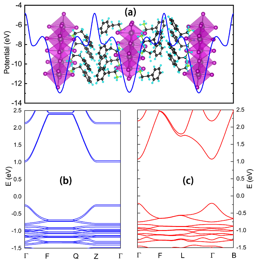
In this work, we focus on the typical 2D hybrid perovskite (PEA)2PbI4Hong et al. (1992); Smith et al. (2019); Du et al. (2017); Do et al. (2020). The (PEA)2PbI4 possesses a stable layered structure, which comprises alternatively stacked layers of [PbI6]4- octahedra and long-chain organic molecules C6H5C2H4NH (PEA) as shown in Fig. 1\textcolorblue(a). To determine both the crystalline structures and electronic structures, the first-principles calculations are performed by using the Vienna ab initio simulation package (VASP) within the generalized gradient approximation (GGA) in Perdew-Burke-Ernzerhof (PBE) type and the projector augmented-wave (PAW) pseudopotential. The kinetic energy cutoff is set to 500 eV for wave-function expansion, and the Monkhorst-Pack type k-point grid is sampled by sums over 333. For the convergence of the electronic self-consistent calculations, the total energy difference criterion is set to 10-8 eV. The crystal structure is fully relaxed until the residual forces on atoms are less than 0.01 eV/Å. The spin-orbital coupling effect is taken into consideration, and the van der Waals correction is also included by DFT-D2 method.
From Fig. 1\textcolorblue(a), one can see that the inorganic layers PbI4 are sandwiched between two organic layers, with the effective potential barriers as high as 8.1 eV, as illustrated by the blue solid curves. Such high potential barriers make (PEA)2PbI4 behaves like stacking quantum wells with hard-wall confining potentials. Due to the weak interlayer Van der Waals coupling, we find the electronic structures are similar between the bulk material and its monolayer. The band structures are shown in Fig 1(c) all over high symmetric reciprocal points indicated in the Brillouin zone. The parabolic conduction and valence bands are isolated with bulk bands, and possess a direct band gap estimated as 1.24 eV. The direct band gap feature ensures good performance of (PEA)2PbI4 in optoelectronic devices. Notice that the band structures of the (PEA)2PbI4 monolayer (See Fig. 1\textcolorblue(c)) possess a direct band gap about 1.278 eV at the point. Unlike other 2D materials whose band gap vary significantly as the thickness decrease to monolayer, e.g., the black phosphorous. The dimensionality reduction from bulk to the monolayer limit does not increase the band gap evidently, since the individual monolayer is naturally well confined by the internal potential barriers, and the interlayer Van der Waals coupling is quite weak.
Based on the band structures obtained from the first-principles calculations above, we study the excitons in (PEA)2PbI4 monolayer. The internal motion of exciton is governed by
| (1) |
where the reduced mass , the electron mass , and the hole mass . The electron mass and hole mass are adopted from the first-principles calculated band dispersions along -L path in k-space, respectively. Considering the ultrathin thickness of the (PEA)2PbI4 monolayer, the Keldysh potentialKeldysh (1979) can be used to describe the Coulomb interaction between the electron and hole.
| (2) |
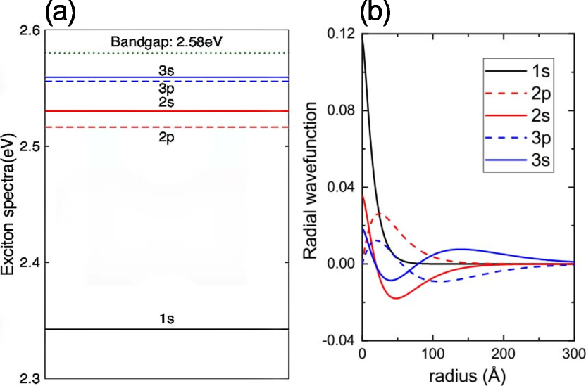
where is the relative displacement between the electron and hole, the screening length of the PbI4 layer , and . The relevant parameters in the Keldysh potential are defined as follows. For the sandwiched inorganic PbI4 layer, the width ÅHong et al. (1992), and the relative permittivity Hong et al. (1992); Ishihara et al. (1990). For the organic barriers, the width Å, and the relative permittivity Hong et al. (1992). The exciton binding energy can be obtained by applying the variational method to Eq.(1). With the parameters given above, the exciton binding energy is about 238.5 meV, which agrees well with the experimental result 220-250meVHong et al. (1992); Cheng et al. (2018). Correspondingly, the exciton spectrum of the (PEA)2PbI4 monolayer (the red solid lines) is shown in Fig. 2\textcolorblue(a). The exciton spectrum is calculated from Eq.(1). The bandgap eV as reported in Ref.Hong et al. (1992), and the PL maximum 2.34eV, which is close to the experimental value 2.4eVHong et al. (1992) and 2.37eVDu et al. (2017).
When a perpendicular electric field is applied, the effective electron-hole interaction becomes dependent on the -directional distribution of the electron () and hole (). The Keldysh potential takes the form as
| (3) |
where the dielectric function is expressed as
| (4) |
in the thin film limit. By expanding the equation of exciton motion Eq.(1) into three dimensional(3D) form, the exciton motions under the electric field are obtained,
| (5) |
Here is the displacement of the center of mass (c.m.) of the exciton, is the c.m. mass of the exciton. denotes the single-particle Hamiltonian of the electron(hole) in the inorganic layer under the external electric field . Variational exciton wavefunctionMiller et al. (1985), associated with the th electron and th hole subbands,
| (6) |
is adopted for the 1-type state in Eq.(5), with variational parameters and . The -directional confinements of the electron and hole are included in and (See APPENDIX A).
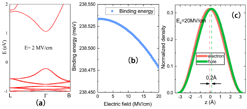
For the 1-type exciton state, the effects of perpendicular electric fields are limited. As shown in Fig 3\textcolorblue(a), The band gap of the perovskite monolayer remains unchanged under an electric field 2 MV/cm. Accordingly, the binding energy of the exciton varies slightly. From Fig 3\textcolorblue(b), one can find the binding energy drops merely 0.06 meV as the strength of the perpendicular electric field increases up to a very strong electric field 20 MV/cm. The reason lies in the fact that, it is difficult to separate electrons and holes vertically, as shown in Fig 3\textcolorblue(c), in presence of perpendicular electric field as strong as 20 MV/cm, the effective spatial separation between centres of holes and electrons along the z-axis is less than 1 . This feature arises from the very strong confining potential (about 8eV) and weak inter-layer coupling.
Although perpendicular electric field changes extremely slightly the binding energies and Bohr radius of the perovskite monolayer, but it is efficient to align dipoles, change the exciton-exciton interactions utterly, and play a crucial role in the exciton BEC under the critical temperature.
The critical temperature for the BEC transition in the flakes of (PEA)2PbI4 monolayer is estimated by
| (7) |
where is the area of the flake, and is the exciton density. For a square flake, with (20nm)2 and 1012cm-2, we obtain K. Therefore, the exciton condensation can be achieved at the temperature under liquid nitrogen regime in (PEA)2PbI4 monolayer.
Usually, the Gross-Pitaevskii (GP) equation is widely used to describe the condensate states. Considering laser pumping and exciton recombination process, the non-equilibrium exciton condensates in the perovskite monolayer with the lateral boundaries, can be described by complex Gross-Pitaevskii (cGP) equation within mean-field approach. Under a weak perpendicular electric field, the exciton-exciton interaction is dominated by repulsive dipole-dipole interaction (DDI), which can be expressed as in reciprocal space,
| (8) |
with . Here is the electron-hole separation introduced by the electric field. Thus the cGP equation is expressed as
| (9) |
where is the pumping rate, the recombination rate, and the exciton lifetime. denotes as the trap potential for excitons. It is worth noting that, convolution of stands for the DDI, which display a nonlinear behavior.
Considering the laser pumping is generally radial symmetric, while the perovskite flakes possess irregular shapes in practice, the disorders induced by the lateral boundary provide the scatterings to the optically generated excitons, and change the directions of their momentum. As a consequence, non-zero angular velocities appear at the edges of the flakes. In presence of the nonlinear DDI term of the flake boundaries, the exciton condensate state is sensitive to the local angular velocities raised by the lateral disorders, which behave as local potentials surrounding the condensate cloud. Therefore, the exciton vortices are expected to emerge in the perovskite monolayer flakes with constant laser pumping.
In order to demonstrate the vortex states, the complex GP equation(9) is solved by time-splitting spectral methods in combination with discrete sine transformsBao and Cai (2015, 2013, 2018); Sierra et al. (2015). The pumping and decaying process in each time step is shown in APPENDIX B. The parameters for exciton vortex simulations in a square flake of (PEA)2PbI4 monolayer with length =400nm, are listed as follows. The flake is sampled by a 512 512 mesh in real space, and the time step is set to be 5ns, to reach high accuracy. The pump power is set to be meV, and the exciton lifetime is =2ns. A shallow harmonic potential is also introduced to mimic interface potential fluctuations in the quantum well structures, i.e., we set for and for , with 10meV and .
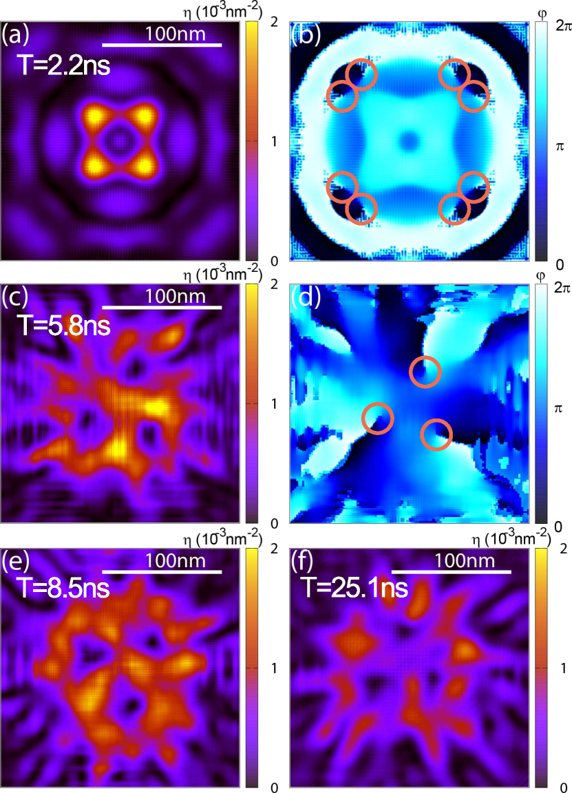
The simulated exciton vortices are shown in Fig. 4. The vortex is characterized by a rotation of the phase of the condensates wavefunction around the singular point by an integer multiple of 2. As shown in Figure 4\textcolorblue(a), the first occasional vortices emerge during the dynamic evolution of the exciton condensates at T = 2.2 ns. The eight vortices locate at the dark spots in the contour plot of the density of the exciton condensates wavefunction. The corresponding phase distributions in Fig. 4\textcolorblue(b), indicate 2 phase shift around the singular points of the wavefunction, which indicate the existence of exciton vortices. As time goes by, the vortex patterns tend to reach dynamic equilibrium since T = 5.8 ns. From Fig. 4\textcolorblue(c) and Fig. 4\textcolorblue(d), one can find there are three vortices in the central area of the perovskite monolayer flake. The three vortices are stable and rotating persistently, as illustrated at T = 8.5 ns, and even T = 25.1 ns, respectively, as shown in Fig. 4\textcolorblue(e) and Fig. 4\textcolorblue(f). Since the evolution time of vortices patterns is comparable to the exciton lifetime, it is promising to observe exciton vortex patterns in (PEA)2PbI4 monolayers experimentally.
In summary, we study the exciton BEC and its vortices in (PEA)2PbI4 monolayer, and calculated exciton binding energy 238.5 meV is in good agreement with experimental results. We find the perpendicular electric fields change slightly the binding energy and Bohr radius in (PEA)2PbI4 monolayer, but are efficient to align the electron-hole dipoles. With laser pumping, the repulsive dipole-dipole interaction created by the perpendicular electric field can drive the laterally confined excitons into various vortex patterns. The evolution time of those vortices is comparable to the exciton lifetime, and reach a stable pattern with certain number of vortices rotating at the center. Since the large exciton binding energy ensures the critical temperature of the exciton BEC within the liquid nitrogen regime, it is possible to realize stable exciton vortices in two-dimensional hybrid perovskite monolayers.
This work was supported by National Key RD Programmes of China, Grant No. 2017YFA0303400, 2016YFE0110000. National Natural Science Foundation of China, Grant No. 11574303, 11504366. Youth Innovation Promotion Association of Chinese Academy of Sciences, Grant No. 2018148, and the Strategic Priority Research Program of Chinese Academy of Sciences, Grant No. XDB28000000.
Appendix A Solution of the quantum confined exciton under electric field
The single particle denotes the Hamiltonian of the electron(hole) in the inorganic layer under the electric field , i.e.,
| (10) |
where is the infinite-potential-barrier for the electron and the hole, since they are confined in the single inorganic layer. Eigenstates of Eq.(10) are represented by the Airy functions Ai and Bi,
| (11) |
where is the subband index of the electron(hole), and
| (12) |
Here is the -th electron (-th hole) subband energy. The parameters are normalized as
, with . The eigenenergies are determined by the -zeros of
| (13) |
Appendix B Treatment of the pumping and decaying term
Here we deal with the time step containing the pumping and decaying term , which can be written as
| (14) |
Since the Eq.(14) is real, we have
| (15) |
Next we solve from Eq.(15), and obtain
| (16) |
with
Recalling Eq.(14),
| (17) |
Putting Eq.(16) into the integral in Eq.(17), we have
| (18) |
The second-order time splitting can be written as
| (19) |
References
- Snoke et al. (1990) D. W. Snoke, J. P. Wolfe, and A. Mysyrowicz, Phys. Rev. Lett. 64, 2543 (1990).
- Butov et al. (2002) L. V. Butov, C. W. Lai, A. L. Ivanov, A. C. Gossard, and D. S. Chemla, Nature 417, 47 (2002).
- Butov et al. (1994) L. V. Butov, A. Zrenner, G. Abstreiter, G. Bohm, and G. Weimann, Phys. Rev. Lett. 73, 304 (1994).
- Rayfield and Reif (1964) G. W. Rayfield and F. Reif, Phys. Rev. 136, A1194 (1964).
- Yarmchuk et al. (1979) E. J. Yarmchuk, M. J. V. Gordon, and R. E. Packard, Phys. Rev. Lett. 43, 214 (1979).
- Keeling and Berloff (2008) J. Keeling and N. G. Berloff, Phys. Rev. Lett. 100, 250401 (2008).
- Lagoudakis et al. (2009) K. G. Lagoudakis, T. Ostatnický, A. V. Kavokin, Y. G. Rubo, R. André, and B. Deveaud-Plédran, Science 326, 974 (2009).
- Roy et al. (2019) I. Roy, S. Dutta, A. N. Roy Choudhury, S. Basistha, I. Maccari, S. Mandal, J. Jesudasan, V. Bagwe, C. Castellani, L. Benfatto, and P. Raychaudhuri, Phys. Rev. Lett. 122, 047001 (2019).
- Chen et al. (ress) Y. D. Chen, Y. W. Huang, W. K. Lou, Y. Y. Cai, and K. Chang, Phys. Rev. B 00, LP16278B (in press).
- Kojima et al. (2009) A. Kojima, K. Teshima, Y. Shirai, and T. Miyasaka, J. Am. Chem. Soc. 131, 6050 (2009).
- You et al. (2013) J. You, L. Dou, K. Yoshimura, T. Kato, K. Ohya, T. Moriarty, K. Emery, C.-C. Chen, J. Gao, G. Li, and Y. Yang, Nat. Commun. 4, 1446 (2013).
- Zhou et al. (2014) H. Zhou, Q. Chen, G. Li, S. Luo, T.-b. Song, H.-S. Duan, Z. Hong, J. You, Y. Liu, and Y. Yang, Science 345, 542 (2014).
- Zhao et al. (2019) W.-Y. Zhao, Z.-L. Ku, L.-P. Lv, X. Lin, Y. Peng, Z.-M. Jin, G.-H. Ma, and J.-Q. Yao, Chin. Phys. Lett. 36, 028401 (2019).
- Jena et al. (2019) A. K. Jena, A. Kulkarni, and T. Miyasaka, Chem. Rev. 119, 3036 (2019).
- Nayak et al. (2019) P. K. Nayak, S. Mahesh, H. J. Snaith, and D. Cahen, Nat. Rev. Mater. 4, 269 (2019).
- Tennyson et al. (2019) E. M. Tennyson, T. A. S. Doherty, and S. D. Stranks, Nat. Rev. Mater. 4, 573 (2019).
- Xie et al. (2017) W.-R. Xie, B. Liu, T. Tao, G.-G. Zhang, B.-H. Zhang, Z.-L. Xie, P. Chen, D.-J. Chen, and R. Zhang, Chin. Phys. Lett. 34, 068103 (2017).
- Grancini and Nazeeruddin (2019) G. Grancini and M. K. Nazeeruddin, Nat. Rev. Mater. 4, 4 (2019).
- Quan et al. (2016) L. N. Quan, M. Yuan, R. Comin, O. Voznyy, E. M. Beauregard, S. Hoogland, A. Buin, A. R. Kirmani, K. Zhao, A. Amassian, D. H. Kim, and E. H. Sargent, J. Am. Chem. Soc. 138, 2649 (2016).
- Li et al. (2018) Z. Li, T. R. Klein, D. H. Kim, M. Yang, J. J. Berry, M. F. A. M. van Hest, and K. Zhu, Nat. Rev. Mater. 3, 18017 (2018).
- Lee et al. (2012) M. M. Lee, J. Teuscher, T. Miyasaka, T. N. Murakami, and H. J. Snaith, Science 338, 643 (2012).
- Ishihara et al. (1990) T. Ishihara, J. Takahashi, and T. Goto, Phys. Rev. B 42, 11099 (1990).
- Hong et al. (1992) X. Hong, T. Ishihara, and A. V. Nurmikko, Phys. Rev. B 45, 6961 (1992).
- Yaffe et al. (2015) O. Yaffe, A. Chernikov, Z. M. Norman, Y. Zhong, A. Velauthapillai, A. van der Zande, J. S. Owen, and T. F. Heinz, Phys. Rev. B 92, 045414 (2015).
- Fang et al. (2020) H.-H. Fang, J. Yang, S. Adjokatse, E. Tekelenburg, M. E. Kamminga, H. Duim, J. Ye, G. R. Blake, J. Even, and M. A. Loi, Adv. Func. Mater. 30, 1907979 (2020).
- Smith et al. (2019) M. D. Smith, B. A. Connor, and H. I. Karunadasa, Chem. Rev. 119, 3104 (2019).
- Du et al. (2017) K.-z. Du, Q. Tu, X. Zhang, Q. Han, J. Liu, S. Zauscher, and D. B. Mitzi, Inorg. Chem. 56, 9291 (2017).
- Do et al. (2020) T. T. H. Do, A. Granados del Águila, D. Zhang, J. Xing, S. Liu, M. A. Prosnikov, W. Gao, K. Chang, P. C. M. Christianen, and Q. Xiong, Nano Lett. 20, 5141 (2020).
- Keldysh (1979) L. V. Keldysh, Soviet Physics JETP 29, 658 (1979).
- Cheng et al. (2018) B. Cheng, T.-Y. Li, P. Maity, P.-C. Wei, D. Nordlund, K.-T. Ho, D.-H. Lien, C.-H. Lin, R.-Z. Liang, X. Miao, I. A. Ajia, J. Yin, D. Sokaras, A. Javey, I. S. Roqan, O. F. Mohammed, and J.-H. He, Commun. Phys. 1, 80 (2018).
- Miller et al. (1985) D. A. B. Miller, D. S. Chemla, T. C. Damen, A. C. Gossard, W. Wiegmann, T. H. Wood, and C. A. Burrus, Phys. Rev. B 32, 1043 (1985).
- Bao and Cai (2015) W. Bao and Y. Cai, SIAM J. Appl. Math. 75, 492 (2015).
- Bao and Cai (2013) W. Bao and Y. Cai, Kinet. Relat. Mod. 6, 1 (2013).
- Bao and Cai (2018) W. Bao and Y. Cai, Commun. Comput. Phys. 24, 899 (2018).
- Sierra et al. (2015) J. Sierra, A. Kasimov, P. Markowich, and R.-M. Weishäupl, J. Nonlinear Sci. 25, 709 (2015).