Experimental observation of Dirac cones in artificial graphene lattices
Abstract
Artificial lattices provide a tunable platform to realize exotic quantum devices. A well-known example is artificial graphene (AG), in which electrons are confined in honeycomb lattices and behave as massless Dirac fermions. Recently, AG systems have been constructed by manipulating molecules using scanning tunnelling microscope tips, but the nanoscale size typical for these constructed systems are impossible for practical device applications and insufficient for direct investigation of the electronic structures using angle-resolved photoemission spectroscopy (ARPES). Here, we demonstrate the synthesis of macroscopic AG by self-assembly of C60 molecules on metal surfaces. Our theoretical calculations and ARPES measurements directly confirm the existence of Dirac cones at the () points of the Brillouin zone (BZ), in analogy to natural graphene. These results will stimulate ongoing efforts to explore the exotic properties in artificial lattices and provide an important step forward in the realization of novel molecular quantum devices.
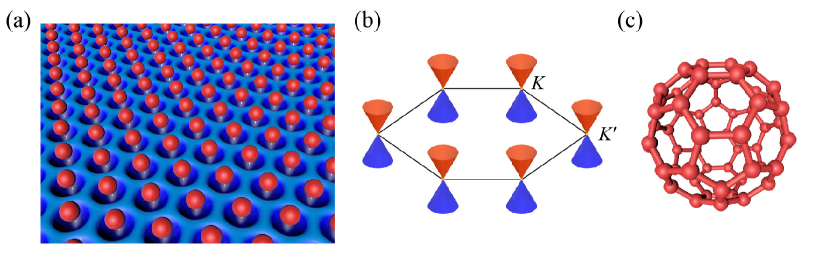
Graphene is a single layer of carbon atoms with a honeycomb lattice, and it has been intensively studied in the past decade GeimAG2007 ; NetoAH2009 . In the proximity of the Fermi level, the electrons in graphene behave as massless Dirac fermions. This is the origin of graphene’s various exotic properties, such as half-integer quantum Hall effects NovoselovKS2005 ; ZhangY2005 and the Klein paradox KatsnelsonMI2006 ; YoungAF2009 ; GutierrezC2016 . An alternative way to realize the exotic properties of graphene is by confining the electrons of a two-dimensional electron gas (2DEG) to an equivalent honeycomb lattice, called artificial graphene (AG) GomesKK2012 ; WangS2014 ; NantohM2017 . Because of the confinement, there exists a Dirac cone at each point of the BZ. As a result, electrons of the otherwise 2DEG behave as massless Dirac fermions, which is analogous to the case of natural graphene. In addition to possessing the novel properties of graphene, artificial lattices possess various tunable parameters, thereby providing an ideal platform for the simulation of quantum behaviours in two-dimensional (2D) Dirac materials SinghaA2011 ; TarruellL2012 ; PoliniM2013 ; KempkesSN2019 ; KempkesSN2019' .
Some molecules, such as carbon monoxide and coronene, can serve as potential barriers through which the electrons of the 2DEG are forbidden to travel. Therefore, a hexagonally patterned molecular lattice can confine the 2DEG electrons into an equivalent honeycomb lattice and lead to the realization of AG GomesKK2012 ; WangS2014 , as illustrated in Figs. 1(a) and 1(b). In 2012, Gomes et al. constructed the first AG by atomic manipulation of carbon monoxide molecules on Cu(111) and found experimental evidence of massless Dirac fermions by scanning tunnelling spectroscopy GomesKK2012 . In addition to the scheme presented by molecular AG, AG has also been realized in nanopatterned GaAs quantum wells GibertiniM2009 ; WangS2016 ; WangS2018 . Unlike unpatterned GaAs quantum wells, resonant inelastic light-scattering spectra of the AG system revealed low-lying transitions that might arise from the Dirac bands WangS2018 . The high energy and momentum resolution of ARPES makes it a powerful technique to directly study the electronic structures of materials. However, direct experimental observation of the Dirac cones in AG using ARPES has not yet been reported.
Here, we constructed macroscopic AG systems by growing monolayer C60 molecules on the (111)-terminated surfaces of noble metals, which enabled ARPES studies of the electronic band structure. Our low-energy electron diffraction (LEED) and ARPES measurements show that these AG systems are homogeneous. Therefore, their size is only limited by the scale of the substrates. The Dirac cones at the () points were directly observed by our ARPES measurements. In addition, we performed model calculations on these AG systems, whose results fully supported our experimental observations.
The lattice constant of nanopatterned structures is typically tens of hundreds of nanometres, which is several orders of magnitude larger than that of conventional single crystals GibertiniM2009 ; WangS2016 ; WangS2018 . Such a large lattice constant results in a very small BZ that is beyond the resolution of conventional ARPES facilities. The molecular AG system is ideal for the investigation of electronic structures because of its moderate lattice constants. However, the size of conventional AG systems constructed by atomic/molecular manipulation is limited to the nanoscale, which is typically insufficient for practical device applications and for electronic band structure investigation. A promising route to realize macroscopic AG is by preparing a molecular self-assembled monolayer on a metal substrate; where such supramolecular architectures can be well ordered across the entire substrate surface. A particular interesting molecule is C60, which has a nearly-isotropic spherical shape, as shown in Fig. 1(c). Previous works have shown that C60 molecules can form hexagonal structures on various noble metal surfaces, including Cu(111), Au(111), and Ag(111). In these systems, the electrons of the 2DEG of the metal surfaces are confined in an equivalent honeycomb lattice and are thus expected to behave as massless Dirac fermions.
First, we studied C60 monolayers on Cu(111). The C60 molecules form a hexagonal structure with a 44 superstructure with respect to the 11 lattice of Cu(111) TamaiA2008 ; PaiWW2010 . The low-energy electron diffraction (LEED) patterns of the C60 monolayer on Cu(111) are shown in Fig. S1 SM . The BZs of the C60 monolayer and of Cu(111) are schematically drawn in Fig. 2(a). Based on the above discussion, this system is expected to be an AG with a lattice constant of 10 Å. Figure 2(b) shows the ARPES intensity of the Fermi surface. The Shockley surface state of Cu(111) almost disappears because of the coverage of the C60 molecules. Instead, a dot-like spectral weight can be seen at each () point. Such features do not exist on pristine Cu(111) because pristine Cu(111) only exhibits Shockley surface states at the BZ centre and bulk bands at the BZ boundary. At deeper binding energies, the dots become closed circles and their size increases as the binding energies increase, as shown in Fig. 2(c)–2(e).
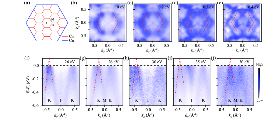
Figure 2(f) shows the ARPES spectra along the – direction. One can observe linearly dispersing bands at the point, as indicated by the red dashed lines (Fig. 1(f)). The fitted crossing point is located approximately 0.1 eV above the Fermi level. Along the –– direction, the dispersion of the bands is also linear, as shown in Fig. 1(g). Combined with the evolution of the constant energy contours, we can conclude that there is a Dirac cone at each point. The Dirac point is located above the Fermi level, and therefore the upper portion of the Dirac cone is inaccessible by conventional ARPES. The upward shift of the Dirac point may originate from the high electron affinity of the C60 molecules, which leads to a significant charge transfer from the substrate to the C60 molecules ModestiS1993 . The Fermi velocity along the – direction is approximately 4105 m/s, which is slightly smaller than that of natural graphene. In addition, the Dirac bands do not disperse with different photon energies, as shown in Figs. 2(h)–2(j), which agrees with their 2D character. Therefore, the ARPES results confirm that the C60/Cu(111) system is an AG with Dirac cones at the () points of the BZ.
We then performed model analysis to understand the physics of the AG system. We note that the Cu(111) surface hosts Shockley-type surface states inside an inverted energy gap at the centre of the BZ, and is thus a model 2DEG system. This is the reason for the success in the construction of AG by atomic/molecular manipulation GomesKK2012 ; WangS2014 . The Hamiltonian of a 2DEG can be described as:
| (1) |
where is the electron effective mass, the reduced Planck constant, and the vector differential operator. For the Cu(111) surface, is approximately 0.38. The eigenvalues and eigenstates can be determined using =/ and =eikr/, where is the volume of the primitive cell, the electron momentum, and the electron position. To simplify the analysis, we used a periodic potential to simulate the effects of the C60 monolayer. The Hamiltonian of the modulated 2DEG can be given as
| (2) |
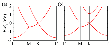
where (=1,2…6) are the six nearest reciprocal lattice vectors. To simplify the analysis, the C60 molecule can be treated as an isotropic sphere. Therefore, the C60/Cu(111) system possesses symmetry and all should be equal; , . As a result, the band structures of the system can be solved numerically. When the interaction between C60 and Cu(111) is turned off, the parabolic bands of 2DEG are simply folded into the BZ of the C60 superstructure, as shown in Fig. 3(a). With a proper value such as 0.4 eV, the Dirac cone at the () point emerges and resembles that of natural graphene, as shown in Fig. 3(b). The calculated Fermi velocity along the – direction is approximately 6.27105 m/s, which is close to the experimental value (4105 m/s). It should be noted that the calculated Fermi velocity of the Dirac cone is insensitive to the variation of U0 (See Supplemental Material, Supplemental Equations E1–E8 and Fig. S2 for details SM ).
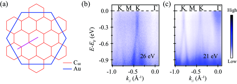
The success of realizing AG in the C60/Cu(111) system provides a universal method for the realization of AG using other noble metal substrates. Another prototypical 2DEG system is Au(111), on which C60 molecules can also form ordered monolayer structures AltmanEI1992 ; WangLL2004 ; HamadaI2011 . Because of the larger lattice constant of Au(111) (=2.9 Å) compared with that of Cu(111) (=2.5 Å), the C60 molecules form a 22 superstructure with respect to the 11 lattice of Au(111). This different superstructure provides further evidence for the universality of this method. As expected, our ARPES results show the existence of Dirac cones at each () point of the BZ, as shown in Fig. 4(b) and 4(c). The Dirac bands do not disperse with varying photon energy, which again agrees with their 2D character. In addition, the Dirac point of the C60/Au(111) system is located approximately 0.2 eV below the Fermi level, and therefore the upper Dirac cone can be observed by our ARPES measurements. The higher binding energy of the Dirac point in the C60/Au(111) system may originate from the smaller charge transfer from the substrate to C60. This is reasonable because the electron affinity of gold is higher than that of copper. The Fermi velocity along the –K direction is approximately 1.2106 m/s, which is slightly higher than that of natural graphene.
Finally, we discuss possible device applications based on these AG systems. First, Cu and Au are commonly used conducting materials, such as electrodes. After depositing a monolayer C60, the emergence of 2D Dirac fermions enable the realization of Klein tunneling KatsnelsonMI2006 ; YoungAF2009 ; GutierrezC2016 , that is, the electrons pass unimpeded through potential barriers. This is crucial component in fabricating low-dissipation quantum devices. Second, noble metals, including Au and Cu, are well-known plasmonic materials with strong visible light response JainPK2007 . The emergence of 2D Dirac fermions on noble metal surfaces indicates the possibility of realizing Dirac plasmon LvJ2011 ; ChenJ2012 in the visible light region, which can be widely used in optoelectronic devices. Notably, plasmonic devices with visible light response is difficult to realize using natural graphene.
All of our results support the realization of AG in the self-assembled C60 monolayer on noble metal surfaces. The Dirac cones at the () points of the BZ are directly observed by our ARPES measurements. The realization of AG in molecular self-assembled monolayers offers new opportunities for the fabrication of exotic molecular quantum devices. Because of the high tunability of supramolecular architectures, such molecular AG systems can also enable the investigation of Dirac fermions under various conditions, such as doping and symmetry breaking, by choosing appropriate molecules, dopants, and substrates. It should be noted that the bulk and thin film of C60 will become a high-temperature superconductor with appropriate alkali metal doping HebardAF1991 ; RenMQ2020 ; CepekC2001 . Therefore, it is highly anticipated that the doped C60 monolayer will host rich physics that originate from the interplay between Dirac fermions and superconductivity; these interesting properties can be probed by various experimental techniques, such as transport, scanning tunneling spectroscopy, and ARPES.
Acknowledgments
This work was supported by the Ministry of Science and Technology of China (Grant No. 2018YFE0202700), the National Natural Science Foundation of China (Grants No. 11974391, No. 11825405, No. 1192780039, No. 11761141013), the Beijing Natural Science Foundation (Grant No. Z180007), and the Strategic Priority Research Program of the Chinese Academy of Sciences (Grants No. XDB33030100 and No. XDB30000000). The synchrotron ARPES measurements were performed with the approval of the Proposal Assessing Committee of Hiroshima Synchrotron Radiation Center (Proposal Numbers: 19AG005 and 19BG028).
S.Y. and H.Z. contributed equally to this work.
References
- (1) A. K. Geim and K. S. Novoselov, The rise of graphene. Nat. Mater. 6, 183-191 (2007).
- (2) A. H. Castro Neto, F. Guinea, N. M. R. Peres, K. S. Novoselov, and A. K. Geim, The electronic properties of graphene. Rev. Mod. Phys. 81, 109-162 (2009).
- (3) K. S. Novoselov, A. K. Geim, S. V. Morozov, D. Jiang, M. I. Katsnelson, I. V. Grigorieva, S. V. Dubonos, and A. A. Firsov, Two-dimensional gas of massless Dirac fermions in graphene. Nature 438, 197-200 (2005).
- (4) Y. Zhang, J. W. Tan, H. L. Stormer, and P. Kim, Experimental observation of the quantum Hall effect and Berry’s phase in graphene. Nature 438, 201-204 (2005).
- (5) M. I. Katsnelson, K. S. Novoselov, and A. K. Geim, Chiral tunnelling and the Klein paradox in graphene. Nat. Phys. 2, 620-625 (2006).
- (6) A. F. Young and P. Kim, Quantum interference and Klein tunnelling in graphene heterojunctions. Nat. Phys. 5, 222-226 (2009).
- (7) C. Gutiérrez, L. Brown, C.-J. Kim, J. Park, and A. N. Pasupathy, Klein tunnelling and electron trapping in nanometre-scale graphene quantum dots. Nat. Phys. 12, 1069 (2016).
- (8) K. K. Gomes, W. Mar, W. Ko, F. Guinea, and H. C. Manoharan, Designer Dirac fermions and topological phases in molecular graphene. Nature 483, 306-310 (2012).
- (9) S. Wang, L. Z. Tan, W. Wang, S. G. Louie, and N. Lin, Manipulation and characterization of aperiodical graphene structures created in a two-dimensional electron gas. Phys. Rev. Lett. 113, 196803 (2014).
- (10) M. Nantoh, K. Takashima, T. Yamamoto, and K. Ishibashi, Sublattice site dependence of local electronic states in superstructures of CO built on a Cu(111) surface. Phys. Rev. B 96, 035424 (2017).
- (11) A. Singha, M. Gibertini, B. Karmakar, S. Yuan, M. Polini, G. Vignale, M. I. Katsnelson, A. Pinczuk, L. N. Pfeiffer, K. W. West, and V. Pellegrini, Two-dimensional Mott-Hubbard electrons in an artificial honeycomb lattice. Science 332, 1176-1179 (2011).
- (12) L. Tarruell, D. Greif, T. Uehlinger, G. Jotzu, and T. Esslinger, Creating, moving and merging Dirac points with a Fermi gas in a tunable honeycomb lattice. Nature 483, 302-305 (2012).
- (13) M. Polini, F. Guinea, M. Lewenstein, H. C. Manoharan, and V. Pellegrini, Artificial honeycomb lattices for electrons, atoms and photons. Nat. Nanotechnol. 8, 625-633 (2013).
- (14) S. N. Kempkes, M. R. Slot, J. J. van den Broeke, P. Capiod, W. A. Benalcazar, D. Vanmaekelbergh, D. Bercioux, I. Swart, and C. M. Smith, Robust zero-energy modes in an electronic higher-order topological insulator. Nat. Mater. 18, 1292-1297 (2019).
- (15) S. N. Kempkes, M. R. Slot, S. E. Freeney, S. J. M. Zevenhuizen, D. Vanmaekelbergh, I. Swart, and C. M. Smith, Design and characterization of electrons in a fractal geometry. Nat. Phys. 15, 127-131 (2019).
- (16) M. Gibertini, A. Singha, V. Pellegrini, and M. Polini, Engineering artificial graphene in a two-dimensional electron gas. Phys. Rev. B 79, 241406(R) (2009).
- (17) S. Wang, D. Scarabelli, Y. Y. Kuznetsova, S. J. Wind, A. Pinczuk, V. Pellegrini, M. J. Manfra, G. C. Gardner, L. N. Pfeiffer, and K. W. West, Observation of electron states of small period artificial graphene in nano-patterned GaAs quantum wells. Appl. Phys. Lett. 109, 113101 (2016).
- (18) S. Wang, D. Scarabelli, L. Du, Y. Y. Kuznetsova, L. N. Pfeiffer, K. W. West, G. C. Gardner, M. J. Manfra, V. Pellegrini, S. J. Wind, and A. Pinczuk, Observation of Dirac bands in artificial graphene in small-period nanopatterned GaAs quantum wells. Nat. Nanotechnol. 13, 29-33 (2018).
- (19) A. Taimi, A. P. Seitsonen, F. Baumberger, M. Hengsberger, Z.-X. Shen, T. Greber, and J. Osterwalder, Electronic structure at the C60/metal interface: An angle-resolved photoemission and first-principles study. Phys. Rev. B 77, 075134 (2008).
- (20) W. W. Pai, H. T. Jeng, C.-M. Cheng, C.-H. Lin, X. Xiao, A. Zhao, X. Zhang, G. Xu, X. Q. Shi, M. A. Van Hove, C.-S. Hsue, and K.-D. Tsuei, Optimal electron doping of a C60 monolayer on Cu(111) via interface reconstruction. Phys. Rev. Lett. 104, 036103 (2010).
- (21) See Supplemental Material at [URL] for experimental methods and analytical solution of the AG model.
- (22) S. Modesti, S. Cerasari, and P. Rudolf, Determination of charge states of C60 adsorbed on metal surfaces. Phys. Rev. Lett. 71, 2469-2472 (1993).
- (23) E. I. Altman and R. J. Colton, Nucleation, growth, and structure of fullerene films on Au(111). Surf. Sci. 279, 49-67 (1992).
- (24) L.-L. Wang and H.-P. Cheng, Density functional study of the adsorption of a C60 monolayer on Ag(111) and Au(111) surfaces. Phys. Rev. B 69, 165417 (2004).
- (25) I. Hamada and M. Tsukada, Adsorption of C60 on Au(111) revisited: A van der Waals density functional study. Phys. Rev. B 83, 245437 (2011).
- (26) P. K. Jain, X. Huang, I. H. El-Sayed, and M. A. El-Sayed, Review of some interesting surface plasmon resonance-enhanced properties of noble metal nanoparticles and their applications to biosystems. Plasmonics 2, 107 (2007).
- (27) L. Ju, B. Geng, J. Horng, C. Girit, M. Martin, Zhao Hao, H. A. Bechtel, X. Liang, A. Zettl, Y. R. Shen, and F. Wang, Graphene plasmonics for tunable terahertz metamaterials. Nat. Nanotechnol. 6, 630-634 (2011).
- (28) C. Chen, et al. Optical nano-imaging of gate-tunable graphene plasmons. Nature 487, 77-81 (2012).
- (29) A. F. Hebard, M. J. Rosseinsky, R. C. Haddon, D. W. Murphy, S. H. Glarum, T. T. M. Palstra, A. P. Ramirez, and A. R. Kortan, Superconductivity at 18 K in potassium-doped C60. Nature 350, 600-601 (1991).
- (30) M.-Q. Ren, S. Han, S.-Z. Wang, J.-Q. Fan, C.-L. Song, X.-C. Ma, and Q.-K. Xue, Direct observation of full-gap superconductivity and pseudogap in two-dimensional fullerides. Phys. Rev. Lett. 124, 187001 (2020).
- (31) C. Cepek, I. Vobornik, A. Goldoni, E. Magnano, G. Selvaggi, J. Kröger, G. Panaccione, G. Rossi, and M. Sancrotti, Temperature-dependent Fermi gap opening in the c(64)-C60/Ag(100) two-dimensional superstructure. Phys. Rev. Lett. 86, 3100 (2001).