Symmetry induced phonon renormalization in few layers of 2H-MoTe2 transistors: Raman and first-principles studies
Abstract
Understanding of electron-phonon coupling (EPC) in two dimensional (2D) materials manifesting as phonon renormalization is essential to their possible applications in nanoelectronics. Here we report in-situ Raman measurements of electrochemically top-gated 2, 3 and 7 layered 2H-MoTe2 channel based field-effect transistors (FETs). While the E and B2g phonon modes exhibit frequency softening and linewidth broadening with hole doping concentration (p) up to 2.3 1013/cm2, A1g shows relatively small frequency hardening and linewidth sharpening. The dependence of frequency renormalization of the E mode on the number of layers in these 2D crystals confirms that hole doping occurs primarily in the top two layers, in agreement with recent predictions. We present first-principles density functional theory (DFT) analysis of bilayer MoTe2 that qualitatively captures our observations, and explain that a relatively stronger coupling of holes with E or B2g modes as compared with the A1g mode originates from the in-plane orbital character and symmetry of the states at valence band maximum (VBM). The contrast between the manifestation of EPC in monolayer MoS2 and those observed here in a few-layered MoTe2 demonstrates the role of the symmetry of phonons and electronic states in determining the EPC in these isostructural systems.
I Introduction
The discovery of unique and remarkable properties of graphene has sparked unprecedented interest in other classes of two dimensional (2D) materials like transition metal dichalcogenides (TMDs, MX2, where M= transition metals (Mo, W, Ti, Nb, Ta) and X= chalcogens (S, Se, Te)) for their potential applications in nano and opto-electronics [1]. Optical and electrical properties of these TMDs can be easily manipulated by both changing the layer number and carrier doping. MoTe2 is a member of the group-VI TMD family that crystallizes into three stable phases: Hexagonal ( or 2H) [2], monoclinic ( or 1T′) [3] and orthorhombic ( or Td) [4]. The 2H phase is semiconducting [5], whereas the 1T′ phase is a narrow band gap semiconductor [6]. Similar to other group-VI dichalcogenides, 2H-MoTe2 has a trigonal-prismatic coordinated crystal structure [7], consisting of weakly coupled sandwich layers of Te-Mo-Te units, where Mo-atom layer is enclosed between two Te layers (Fig. 1(a)) [2]. Unlike other TMDs, energy difference between the 2H and 1T′ phase is very small ( 31 meV per formula unit [8]). This enables easy tuning of the two phases by strain [9, 10], laser irradiation [11, 12] and electron doping [13, 14], making this material an ideal candidate for next generation homojunction devices [15]. From electron doping (n) induced transition from 2H to 1T′ phase in multilayer MoTe2, Zakhidov et al. recently suggested that doped electrons by ionic liquid (IL) gating are localized on the top few layers of the nanocrystal [14], consistent with previous theoretical calculations [16].
Bulk MoTe2 has an indirect band gap of 1.0 eV [18, 19] which becomes a direct band gap semiconductor in a monolayer with an emission peak of excitonic photoluminescence (PL) spectrum in the near-infrared range ( 1.1 eV) [5]. This enables the material to be a highly sensitive photodetector [20, 21] and light-emitting diode [22, 23]. With device performance at par with its sister compounds MoS2 and MoSe2 [24], MoTe2 shows ambipolar transport properties [25], which has been recently implemented as a p-n homojunction rectifier device with low charge trapping at the junction interface [26]. Since the exploration of these properties has been mostly carried out in monolayer regime, investigation of the charge localization at high gate bias in few layers of the nanocrystal can open up new possibilities in the field of opto-electronics.
Carrier concentration in a semiconductor can be modulated by injecting resonant photons from light emitting diode [27, 28, 29], substitutional doping during growth process [30] and application of an electrostatic field on the channel of a FET [31, 32, 33, 34]. Electrolyte gating has gained immense interest recently for electrostatic modulation of carrier density up to /cm2 [35] owing to their large dielectric capacitance. On application of gate voltage, ions move inside the electrolyte to screen the applied electric field to form few Angstroms [36] thick double layers of ions near the device and gate electrode [37, 38]. However electrolyte gating is well known source of electrostatic disorders [39, 40] and is best suited for disorder robust systems such as superconductors [41, 42].
As Raman spectroscopy does not require any sample preparation, it has been extensively used as a non-invasive, contact-less, fast and accurate tool to determine strain [43], doping effects [13], layer number [44, 17], crystal orientation [45], structural transitions between different polytypes [46, 47, 9, 13, 14, 11, 12, 48] in fewlayer MoTe2 devices in ambient as well as different sample environments. Furthermore, Raman scattering has been employed in various 2D materials to measure electron-phonon coupling (EPC) that governs electronic transport properties [31, 32]. For n-type semiconducting MoS2, symmetry of the conduction band minimum (CBM) determines EPC of the A1g and E modes [33]. In ambipolar phosphorene transistor, electrons and holes couple differently to phonons as CBM and valence band maximum (VBM) possess different orbital symmetries [34]. Although the electronic band structure of monolayer MoTe2 is similar to MoS2 [16], the VBM of the former remains at the K-point from single to three layers [49, 16]. Thus a study of the EPC in few layer MoTe2, an intrinsic p-type semiconductor [50, 51], will reveal asymmetry of phonon coupling with holes and electrons in these hexagonal polytypes of TMDs.
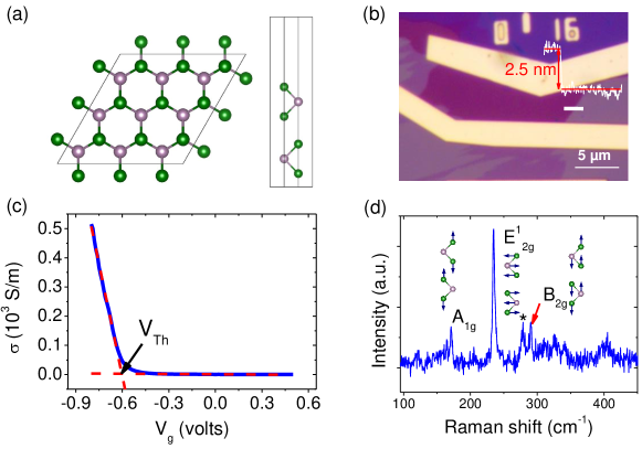
Bulk MoTe2 belongs to D6h point-group [52] having six Raman active modes (A1g+ 2B2g+ E1g+ 2E2g) [17]. A1g and E2g modes have vibrations perpendicular to and along the basal plane of the lattice, respectively [17]. The in-plane E1g mode is absent in backscattering configuration [17]. Notably, the translation symmetry along the z-direction is broken in a few layer nanocrystal, reducing the symmetry to D3h and D3d for odd and even layers of MoTe2, respectively [52]. Thus, the out-of-plane inactive mode B2g in bulk becomes Raman active in few layers and shows highest intensity in a bilayer nanocrystal [53]. For odd layer nanocrystal, the inversion symmetry breaks, making some modes both Raman and infrared active [17]. For simplicity, the Raman modes of even and odd layers of MoTe2 in this paper are represented by the bulk phonon symmetry group of equivalent atomic displacements (see table-S1 of the supplemental material (SM)).
In the present study, we measure in-operando optical phonons in a few layers of 2H-MoTe2 based field-effect transistors (FETs) as a function of hole doping concentration (p) up to 2.31013 cm-2. The modes involving both metal and chalcogen atom vibrations, E and B2g [17] show phonon softening and linewidth broadening while the A1g mode with out-of-plane vibrations of only the chalcogen atoms [17], shows in contrast, relatively smaller phonon hardening and linewidth sharpening. The frequency renormalization comparison of E mode from 2, 3 and 7 layer devices indicate that the doping is confined to only two top layers of the nanocrystal. We have carried out first-principles density functional theory (DFT) calculations on a bilayer MoTe2 transistor for understanding the experimental results. We show that the holes couple weakly with the A1g mode as compared to E and B2g modes and demonstrate that different orbital symmetries of the VBM and CBM at the K-point of MoTe2 and MoS2, respectively, contribute to their contrasting EPC.
II Results and discussion
II.1 Experimental results
Bulk MoTe2 crystals were mechanically exfoliated and transferred to a clean Si/SiO2 (285 nm) substrate. Device contacts were fabricated by first patterning them in electron-beam lithography followed by thermal evaporation of 5 and 50 nm thick chromium and gold respectively. The optical image of the two-probe device is shown in Fig. 1(b). Atomic force microscope (AFM) measurement in tapping mode (inset graph of Fig. 1(b)) confirms the nanocrystal thickness to be 2.5 nm ( 3 monolayers). A drop of 1-ethyl-3-methylimidazolium bis(trifluoromethylsulfonyl)imide (EMIM-TFSI) IL was drop casted on top of the device channel for electrochemical top gating. Electrical measurements were done using a Keithley 2400 source meters. Conductivity () as a function of gate voltage (Vg) shows hole transport (Fig. 1(c)) due to unintentional doping from the environment. Previous experiments done on few layer MoTe2 show formation of Mo-O bonds on tellurium vacancy sites which shift the Fermi level towards the VBM, making MoTe2 intrinsically hole doped [51, 50]. To determine hole doping, p, from Vg, we use parallel plate capacitor formula, , where VTh is the current threshold voltage, and the gate capacitance of the IL, CG is taken to be 5.9 F/cm2 [54]. Consistent with previous reports [55, 56], the device shows field-effect mobility 1.85 cm2/V.s and current on/off ratio 105.
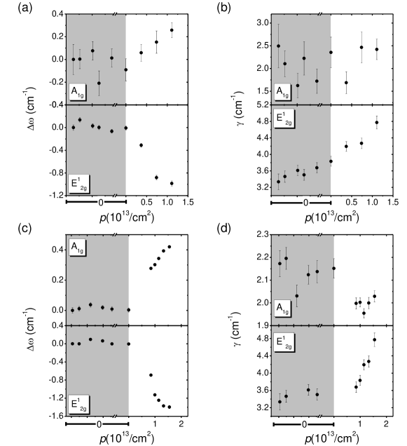
In-situ transport and Raman measurements in backscattering configuration were done at room temperature using LabRAM HR-800 Evolution spectrometer having 1800 lines/mm gratings and a Peltier cooled CCD detector. Excitation laser of 532 nm wavelength was focused using a 50 long working distance objective with incident power less than 0.5 mW to avoid heating. Raman spectrum of the trilayer nanocrystal is shown in Fig. 1(d). At each gate voltage, the peaks are fitted with a sum of Lorentzian functions to extract the phonon frequency () and linewidth (). Figs. 2(a) and (b) show the change in phonon frequency from zero doped state () and linewidth of the trilayer nanocrystal, respectively, with hole doping concentration up to 1.1 1013/cm2. The frequency of the in-plane mode E decreases and linewidth broadens whereas the out-of-plane mode, A1g shows in contrast, relatively small phonon hardening and linewidth sharpening. We have repeated our experiments for a bilayer nanocrystal. We have used a FET device with both bilayer and multilayer channels in parallel to confirm our doping effect in the electrical transfer characteristic (see Fig. S1(a) of the SM). Electrochemical gating induced ions sit very close (few Angstrom [36]) to the semiconductor surface in a FET. Using EMIM-TFSI gating on a hexagonal boron-nitride enclosed strontium titanate (STO), a two-dimensional electron gas system (2DES), Gallagher et al. [40] have shown that disorders induced by the IL reduces the mobility by an order of magnitude. Xia et al. [39] theoretically explained this effect in terms of 2D percolative transport from trapped carriers due to the ions induced by the IL at the semiconductor-electrolyte interface. Hence, the mobility suppression will be higher in monolayer and bilayer channels resulting in negligible transistor performance.
As the intensity of the A1g Raman mode is weak for 532 nm laser excitation for few layers of MoTe2 [5], we have used excitation wavelength of 660 nm (Fig. S1(b) of the SM) for this device. With hole doping concentration up to 1.5 1013/cm2, similar to the trilayer nanocrystal (Figs. 2(a) and (b)), A1g mode shows a trend of phonon hardening and linewidth sharpening to a small extent and the E mode shows phonon softening and linewidth broadening (Figs. 2(c) and (d)). The nature of the A1g mode as reported by Grzeszczyk et al. [44], depends on the thickness of the MoTe2 nanocrystal. They have shown that at 633 nm of laser excitation, A1g is a single peak both in monolayer and bilayer nanocrystals [44]. However, the intensity of the peak drops below E and splits into multiple peaks in multilayer nanocrystals of 2H-MoTe2 [44]. The single peak of the A1g mode in the observed Raman spectrum at 660nm of laser excitation shown in Fig. S1(b) combined with AFM data in Fig. S1(a), confirm that the doping dependence presented in Figs. 2(c) and (d) are indeed from the bilayer part of the device (Fig. S1(a)). In addition, the observed trend of and is similar to the isolated trilayer nanocrystal (Figs. 2(a) and (b)), confirming the effect of hole doping. However, the transfer characteristics shown in Fig. S1(a) is dominated by the multilayer nanocrystal. Furthermore, the threshold voltage for Raman frequency and linewidth shift of the bilayer nanocrystal (Figs. 2(c) and (d)) matches well with the threshold voltage in the transfer characteristics (Fig. S1(a)). It is to be noted that for similar reasons, parallel channels of bulk and monolayer of black phosphorus nanocrystal were used to determine phonon renormalisation with doping [34].
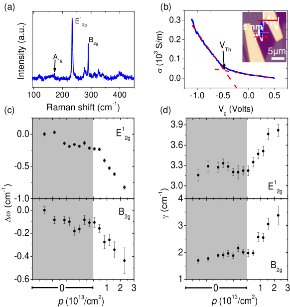
As the frequency of the Raman mode from the IL (see Fig. S2 of the SM ) is close to the B2g mode at 290 cm-1 (Fig. 1(d)), we did experiments on a seven-layer thick nanocrystal, where the Raman signal (with 532 nm wavelength of laser excitation) is more prominent (Fig. 3(a)). Fig. 3(b) shows the thickness of the nanocrystal to be 5 nm ( seven layers) from AFM measurement (inset graph of Fig. 3(b)). The device transfer characteristics in Fig. 3(b) shows hole field-effect mobility of 0.41 cm2/V.s and current on/off ratio 102. Using SiO2 back gate, Pradhan et al. [24], showed similar transistor characteristic of trilayer and seven-layer nanocrystals, since few-layer MoTe2 is an indirect bandgap semiconductor with small change in bandgap from monolayer to bulk [5]. At ambient condition, the seven-layer nanocrystal is initially unintentionally hole doped (Fig. 3(b)) as compared to the trilayer nanocrystal (Fig. 1(c)). Thus the dielectric screening of the gate voltage can account for the relatively smaller mobility and current on-off ratio in seven layer crystal as compared with the trilayer nanocrystal. With hole doping up to , the in-plane vibrational mode, E shows phonon softening and linewidth broadening (Figs. 3(c) and (d)), similar to trilayer and bilayer nanocrystal (Fig. 2). The B2g mode, although having similar vibrational displacements to the A1g mode [17], shows phonon renormalization as the in-plane E mode.
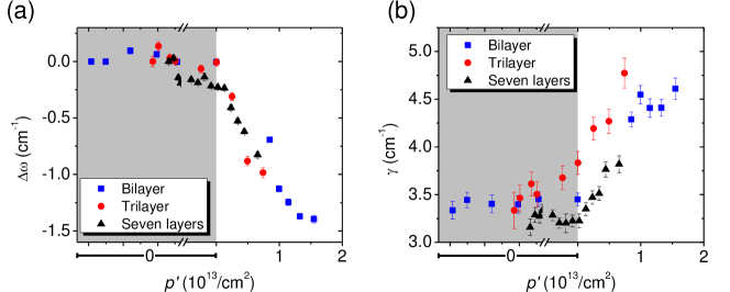
Brumme et al. [16] theoretically showed that the charges localize only in the topmost two layers due to screening effects in MoTe2 based FET devices. From electron doping induced 2H to 1T′ phase transition from bulk to monolayer MoTe2, Zakhidov et al. experimentally showed that the gating by IL causes electrons to be confined in the topmost few layers [14]. Consistent with these reports, we observe a smaller change in and of E mode for a given gate voltage as the layer number increases (Figs. 2, 3(c) and 3(d)). Taking the applied doping (p) to be limited to the top two layers rather than the entire nanocrystal, the average doping () for a N-layer nanocrystal is scaled as . With , of E from 2, 3 and 7 layer nanocrystal scale very well with each other (Fig. 4(a)), justifying that the doping is confined to top two layers of the nanocrystal. The scaling of for the three devices (Fig. 4(b)) is modest with .
II.2 Theoretical analysis
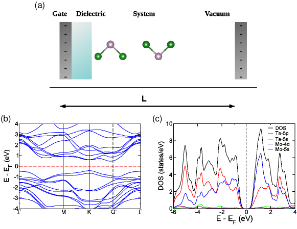
Our first-principles DFT calculations of the bilayer were carried out with Quantum ESPRESSO (QE) package [57], in which we treat only the valence electrons by effectively replacing the potential of ionic cores with pseudopotentials. Exchange-correlation energy of electrons is included within a generalized gradient approximation (GGA) [58] in the functional form parametrized by Perdew, Burke, and Ernzerhof [59]. We include spin-orbit coupling (SOC) through use of relativistic pseudopotentials and a second variational procedure [60]. Kohn-Sham wave functions and charge density were represented in plane wave basis sets truncated at energy cut-offs of 40 Ry and 320 Ry respectively. A vacuum layer of 10 Å has been introduced parallel to MoTe2 layer (perpendicular to z-direction) to weaken the interaction between the layer and its periodic images. Brillouin zone (BZ) integrations were sampled on uniform mesh of k-points. The discontinuity in occupation numbers of electronic states was smeared using a Fermi-Dirac distribution function with broadening temperature of kBT = 0.003 Ry. We include van der Waals (vdW) interaction using PBE + D2 parametrized scheme of Grimme [61].
We have used the FET setup [62] as implemented in QE package to treat gating electric field. A 2D charged plate modeling the gate electrode is placed at z= 0.019 L. A potential barrier with a height of V0 = 0.09 Ry and a width of db = 0.1 L is used to model the dielectric layer, preventing ions from moving too close to the gate electrode (Fig. 5(a)). Dynamical matrices were calculated within the Density Functional Perturbation Theory (DFPT) [63] on a mesh of q-vectors in the Brillouin zone. Fourier interpolation of these dynamical matrices was done to obtain phonon frequencies at arbitrary wavevectors and dispersion along the high symmetry lines in the Brillouin zone.
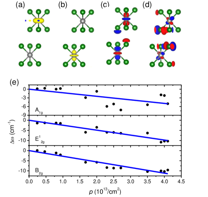
Bilayer 2H-MoTe2 has a hexagonal structure, where covalently bonded layers of Te-Mo-Te atomic planes are stacked along c-axis interacting via weak vdW interaction. The periodic unit cell of bilayer 2H-MoTe2 is characterized by a stacking sequence AbABaB, where Wyckoff positions A, B label basal Te atomic planes and a,b label Mo atomic planes of the hexagonal lattice (Fig. 1(a)). Our estimate of the lattice parameter a (= b) is 3.53 Å which matches well with previous experimental value [64]. Bilayer 2H-MoTe2 is an indirect band gap semiconductor with VBM at K and CBM at Q’ point (along -K direction) separated by a gap of 0.88 eV (Fig. 5(b)). From the projected electronic density of states (DOS) (calculated without SOC) (Fig. 5(c)), it is evident that there is a rather strong coupling between the Mo d orbitals and Te p orbitals, contributing to states near the gap. Visualization of wavefunctions of states at VBM and CBM at and K-points confirms the contribution of specific d-orbitals of Mo and p-orbitals of Te (Fig. 6(a-d)). The doped holes occupy the states at the K-point. With increasing hole-doping, holes continue to accumulate in states at K-point because energy separation between valence band of Q’ valley and valence band states at K-point is rather large ( 490 meV) (Fig. 5(b)). We find that inclusion of SOC in our calculations leads to notable reduction in the indirect band gap by 60 meV and hence we have included SOC in further calculations.
We simulated hole doping in 2H-MoTe2 bilayer by adding a small fraction of holes (close to the experimental doping concentration) to its unit cell. From the changes in calculated frequencies with their linear fits (Fig. 6(e)), it can be seen that for A1g mode is cm -1 for , in contrast to corresponding higher softening of E mode by 10.2 cm-1 and B2g mode by 11.4 cm-1. The magnitude of the slope () for the A1g mode is least, indicating smallest change of this mode frequency (compared to E and B2g ) with doping. Although DFT analysis qualitatively captures the experimental trend of versus for E and B2g (Figs. 2, 3(c) and 3(d)), the relatively smaller phonon hardening observed in experiments for the A1g mode ( as compared to E and B2g modes) is not captured in our DFT analysis.
In order to understand why A1g and B2g are affected differently, we have calculated the EPC of pristine bilayer without inclusion of SOC to understand these trends, as estimation of EPC with doping in FET geometry is not currently implemented in the QE code. The EPC of a mode at momentum q (with frequency q) is calculated as [33]
| (1) |
where and N(f) are the phonon frequency and electronic density of states at the Fermi energy, respectively. The EPC matrix element is given by
| (2) |
where k,j is the electronic wave function with wave vector k and energy eigenvalue k,j for band j, and M is the ionic mass. Vq is the change in the self-consistent potential induced by atomic displacements of phonon q. The calculated values of EPC of B2g and A1g modes are 0.016 and 0.011 respectively, consistent with the experimental observation that B2g phonon is renormalized more with the hole doping.
It is interesting to compare these trends with the phonon renormalization seen in n-doped monolayer MoS2 [33]. Electron doping in monolayer MoS2 has contrasting effects on the frequencies of A1g and E optic modes [33]. While A1g mode softens significantly ( 7 cm-1 at 1.81013/cm2), E remains unaffected [33]. We can understand this contrast as follows: monolayer MoS2 is a direct band-gap semiconductor with a gap of 1.8 eV with the VBM and CBM at the K-point [49]. The CBM at the K-point of MoS2 has contribution from the out-of-plane d orbital of Mo atoms [33]. The A1g mode has the symmetry of the lattice, hence matrix element is non zero [33]. In contrast, matrix element of in-plane vibrational mode E vanishes as it is orthogonal to A1g irreducible representation [33]. In comparison, hole doping in bilayer 2H-MoTe2 leads to occupation of states at the top of the valence band at the K-point, having dominance of in-plane dxy orbitals (odd symmetry states) of Mo. The crystal symmetry at K-point is point group C2 which is a nontrivial subgroup of D3d and the symmetry of the valence band is A2u. The matrix element f Vq i (where i and f are the initial and final electronic wavefunctions) for = A1g, E and B2g modes are non-zero as calculated using direct product table for C2. Hence, changes in occupancy of these states as a function of doping result in renormalization of these modes. Though A1g and B2g modes have different symmetries in bulk, the modes reduce to the same symmetry, A1g in the case of bilayer (symmetry in even layer, odd layer, and bulk MoTe2 has been listed in table S1), softening is stronger for B2g mode as compared to A1g. This is consistent with the EPC being slightly higher for the B2g (0.016) than the A1g (0.011) mode and is also evident in frequency versus hole doping concentration plot (Fig.6(e)).
III Conclusions
In FET devices with 2, 3 and 7 layers of MoTe2 as channels, we have demonstrated that hole doping induces phonon softening and linewidth broadening of the E and B2g modes, while the A1g mode shows relatively small phonon hardening and linewidth sharpening. Due to dielectric screening, we find that holes are induced only in the top two layers of these channels upon electrochemical top gating, as evident in the layer dependent frequency softening of the E mode. Results of our first-principles density functional theory calculations agree qualitatively with our experiments. Interestingly, effects of EPC in hole doped MoTe2 observed here are in sharp contrast to the trends seen earlier in electron doped monolayer MoS2. We explain this in terms of the difference in symmetry of their frontier states relevant to electron and hole doping. In addition to being relevant to use Raman spectroscopy as a non-invasive tool for characterization of MoTe2-FET devices, our study will be useful in understanding the role of relevant phonon interaction with charge carriers in determining carrier mobility in MoTe2 devices.
Acknowledgment
We thank the Centre for Nanoscience and Engineering department (CeNSE) of IISc for device fabrication facilities. AS is thankful to JNCASR for postdoctoral fellowship. AKS thanks Department of Science and Technology (DST), India for support under the Nanomission project and Year of Science Professorship. UVW acknowledges support from a J. C. Bose National Fellowship of SERB-DST, Govt. of India and an AOARD project from United States Air Force.
References
- Wang et al. [2012] Q. H. Wang, K. Kalantar-Zadeh, A. Kis, J. N. Coleman, and M. S. Strano, Nature nanotechnology 7, 699 (2012).
- Puotinen and Newnham [1961] D. Puotinen and R. E. Newnham, Acta Crystallographica 14, 691 (1961).
- Brown [1966] B. E. Brown, Acta Crystallographica 20, 268 (1966).
- Qi et al. [2016] Y. Qi, P. G. Naumov, M. N. Ali, C. R. Rajamathi, W. Schnelle, O. Barkalov, M. Hanfland, S.-C. Wu, C. Shekhar, Y. Sun, et al., Nature communications 7, 1 (2016).
- Ruppert et al. [2014] C. Ruppert, O. B. Aslan, and T. F. Heinz, Nano Letters 14, 6231 (2014).
- Keum et al. [2015] D. H. Keum, S. Cho, J. H. Kim, D.-H. Choe, H.-J. Sung, M. Kan, H. Kang, J.-Y. Hwang, S. W. Kim, H. Yang, et al., Nature Physics 11, 482 (2015).
- Verble and Wieting [1970] J. L. Verble and T. J. Wieting, Phys. Rev. Lett. 25, 362 (1970).
- Li et al. [2016] Y. Li, K.-A. N. Duerloo, K. Wauson, and E. J. Reed, Nature communications 7, 1 (2016).
- Song et al. [2016] S. Song, D. H. Keum, S. Cho, D. Perello, Y. Kim, and Y. H. Lee, Nano Letters 16, 188 (2016).
- Hou et al. [2019] W. Hou, A. Azizimanesh, A. Sewaket, T. Peña, C. Watson, M. Liu, H. Askari, and S. M. Wu, Nature nanotechnology 14, 668 (2019).
- Cho et al. [2015] S. Cho, S. Kim, J. H. Kim, J. Zhao, J. Seok, D. H. Keum, J. Baik, D.-H. Choe, K. J. Chang, K. Suenaga, S. W. Kim, Y. H. Lee, and H. Yang, Science 349, 625 (2015).
- Tan et al. [2018] Y. Tan, F. Luo, M. Zhu, X. Xu, Y. Ye, B. Li, G. Wang, W. Luo, X. Zheng, N. Wu, Y. Yu, S. Qin, and X.-A. Zhang, Nanoscale 10, 19964 (2018).
- Wang et al. [2017] Y. Wang, J. Xiao, H. Zhu, Y. Li, Y. Alsaid, K. Y. Fong, Y. Zhou, S. Wang, W. Shi, Y. Wang, et al., Nature 550, 487 (2017).
- Zakhidov et al. [2020] D. Zakhidov, D. A. Rehn, E. J. Reed, and A. Salleo, ACS Nano 14, 2894 (2020).
- Ma et al. [2019] R. Ma, H. Zhang, Y. Yoo, Z. P. Degregorio, L. Jin, P. Golani, J. Ghasemi Azadani, T. Low, J. E. Johns, L. A. Bendersky, A. V. Davydov, and S. J. Koester, ACS Nano 13, 8035 (2019).
- Brumme et al. [2015] T. Brumme, M. Calandra, and F. Mauri, Phys. Rev. B 91, 155436 (2015).
- Froehlicher et al. [2015] G. Froehlicher, E. Lorchat, F. Fernique, C. Joshi, A. Molina-Sánchez, L. Wirtz, and S. Berciaud, Nano Letters 15, 6481 (2015).
- Conan et al. [1979] A. Conan, D. Delaunay, A. Bonnet, A. G. Moustafa, and M. Spiesser, physica status solidi (b) 94, 279 (1979).
- Grant et al. [1975] A. J. Grant, T. M. Griffiths, G. D. Pitt, and A. D. Yoffe, Journal of Physics C: Solid State Physics 8, L17 (1975).
- Zhang et al. [2017] K. Zhang, X. Fang, Y. Wang, Y. Wan, Q. Song, W. Zhai, Y. Li, G. Ran, Y. Ye, and L. Dai, ACS Applied Materials & Interfaces 9, 5392 (2017).
- Kuiri et al. [2016] M. Kuiri, B. Chakraborty, A. Paul, S. Das, A. K. Sood, and A. Das, Applied Physics Letters 108, 063506 (2016).
- Li et al. [2017] Y. Li, J. Zhang, D. Huang, H. Sun, F. Fan, J. Feng, Z. Wang, and C.-Z. Ning, Nature nanotechnology 12, 987 (2017).
- Bie et al. [2017] Y.-Q. Bie, G. Grosso, M. Heuck, M. M. Furchi, Y. Cao, J. Zheng, D. Bunandar, E. Navarro-Moratalla, L. Zhou, D. K. Efetov, et al., Nature nanotechnology 12, 1124 (2017).
- Pradhan et al. [2014] N. R. Pradhan, D. Rhodes, S. Feng, Y. Xin, S. Memaran, B.-H. Moon, H. Terrones, M. Terrones, and L. Balicas, ACS Nano 8, 5911 (2014).
- Nakaharai et al. [2015] S. Nakaharai, M. Yamamoto, K. Ueno, Y.-F. Lin, S.-L. Li, and K. Tsukagoshi, ACS Nano 9, 5976 (2015).
- Aftab et al. [2019] S. Aftab, M. F. Khan, P. Gautam, H. Noh, and J. Eom, Nanoscale 11, 9518 (2019).
- Li et al. [2019] Q. Li, S. Bi, K. Asare-Yeboah, J. Na, Y. Liu, C. Jiang, and J. Song, ACS Nano 13, 8425 (2019).
- Bi et al. [2020] S. Bi, Q. Li, K. Asare-Yeboah, J. Na, Y. Sun, and C. Jiang, The Journal of Physical Chemistry Letters 11, 3947 (2020).
- Asare-Yeboah et al. [2020] K. Asare-Yeboah, Q. Li, C. Jiang, Z. He, S. Bi, Y. Liu, and C. Liu, The Journal of Physical Chemistry Letters 11, 6526 (2020).
- Yoo et al. [2018] H. Yoo, S. Hong, S. On, H. Ahn, H.-K. Lee, Y. K. Hong, S. Kim, and J.-J. Kim, ACS Applied Materials & Interfaces 10, 23270 (2018).
- Yao et al. [2000] Z. Yao, C. L. Kane, and C. Dekker, Phys. Rev. Lett. 84, 2941 (2000).
- Efetov and Kim [2010] D. K. Efetov and P. Kim, Phys. Rev. Lett. 105, 256805 (2010).
- Chakraborty et al. [2012] B. Chakraborty, A. Bera, D. V. S. Muthu, S. Bhowmick, U. V. Waghmare, and A. K. Sood, Phys. Rev. B 85, 161403 (2012).
- Chakraborty et al. [2016] B. Chakraborty, S. N. Gupta, A. Singh, M. Kuiri, C. Kumar, D. V. S. Muthu, A. Das, U. V. Waghmare, and A. K. Sood, 2D Materials 3, 015008 (2016).
- Yuan et al. [2009] H. Yuan, H. Shimotani, A. Tsukazaki, A. Ohtomo, M. Kawasaki, and Y. Iwasa, Advanced Functional Materials 19, 1046 (2009).
- Lu et al. [2004] C. Lu, Q. Fu, S. Huang, and J. Liu, Nano Letters 4, 623 (2004).
- Gebbie et al. [2015] M. A. Gebbie, H. A. Dobbs, M. Valtiner, and J. N. Israelachvili, Proceedings of the National Academy of Sciences 112, 7432 (2015).
- Jurado and Espinosa-Marzal [2017] L. A. Jurado and R. M. Espinosa-Marzal, Scientific Reports 7, 4225 (2017).
- Xia et al. [2010] Y. Xia, W. Xie, P. P. Ruden, and C. D. Frisbie, Phys. Rev. Lett. 105, 036802 (2010).
- Gallagher et al. [2015] P. Gallagher, M. Lee, T. A. Petach, S. W. Stanwyck, J. R. Williams, K. Watanabe, T. Taniguchi, and D. Goldhaber-Gordon, Nature communications 6, 1 (2015).
- Ueno et al. [2008] K. Ueno, S. Nakamura, H. Shimotani, A. Ohtomo, N. Kimura, T. Nojima, H. Aoki, Y. Iwasa, and M. Kawasaki, Nature Materials 7, 855 (2008).
- Ye et al. [2010] J. T. Ye, S. Inoue, K. Kobayashi, Y. Kasahara, H. T. Yuan, H. Shimotani, and Y. Iwasa, Nature Materials 9, 125 (2010).
- Karki et al. [2020] B. Karki, B. Freelon, M. Rajapakse, R. Musa, S. M. S. Riyadh, B. Morris, U. Abu, M. Yu, G. Sumanasekera, and J. B. Jasinski, Nanotechnology 31, 425707 (2020).
- Grzeszczyk et al. [2016] M. Grzeszczyk, K. Gołasa, M. Zinkiewicz, K. Nogajewski, M. R. Molas, M. Potemski, A. Wysmołek, and A. Babiński, 2D Materials 3, 025010 (2016).
- Song et al. [2017] Q. Song, H. Wang, X. Pan, X. Xu, Y. Wang, Y. Li, F. Song, X. Wan, Y. Ye, and L. Dai, Scientific Reports 7, 1758 (2017).
- Kuiri et al. [2020] M. Kuiri, S. Das, D. V. S. Muthu, A. Das, and A. K. Sood, Nanoscale 12, 8371 (2020).
- Bera et al. [2017] A. Bera, A. Singh, D. V. S. Muthu, U. V. Waghmare, and A. K. Sood, Journal of Physics: Condensed Matter 29, 105403 (2017).
- Zhao et al. [2019] X.-M. Zhao, H.-y. Liu, A. F. Goncharov, Z.-W. Zhao, V. V. Struzhkin, H.-K. Mao, A. G. Gavriliuk, and X.-J. Chen, Phys. Rev. B 99, 024111 (2019).
- Splendiani et al. [2010] A. Splendiani, L. Sun, Y. Zhang, T. Li, J. Kim, C.-Y. Chim, G. Galli, and F. Wang, Nano Letters 10, 1271 (2010).
- Stan et al. [2020] G. Stan, C. V. Ciobanu, S. R. J. Likith, A. Rani, S. Zhang, C. A. Hacker, S. Krylyuk, and A. V. Davydov, ACS Applied Materials & Interfaces 12, 18182 (2020).
- Qu et al. [2017] D. Qu, X. Liu, M. Huang, C. Lee, F. Ahmed, H. Kim, R. S. Ruoff, J. Hone, and W. J. Yoo, Advanced Materials 29, 1606433 (2017).
- Ribeiro-Soares et al. [2014] J. Ribeiro-Soares, R. M. Almeida, E. B. Barros, P. T. Araujo, M. S. Dresselhaus, L. G. Cançado, and A. Jorio, Phys. Rev. B 90, 115438 (2014).
- Yamamoto et al. [2014] M. Yamamoto, S. T. Wang, M. Ni, Y.-F. Lin, S.-L. Li, S. Aikawa, W.-B. Jian, K. Ueno, K. Wakabayashi, and K. Tsukagoshi, ACS Nano 8, 3895 (2014).
- Misra et al. [2007] R. Misra, M. McCarthy, and A. F. Hebard, Applied Physics Letters 90, 052905 (2007).
- Lin et al. [2014] Y.-F. Lin, Y. Xu, S.-T. Wang, S.-L. Li, M. Yamamoto, A. Aparecido-Ferreira, W. Li, H. Sun, S. Nakaharai, W.-B. Jian, K. Ueno, and K. Tsukagoshi, Advanced Materials 26, 3263 (2014).
- Fathipour et al. [2014] S. Fathipour, N. Ma, W. S. Hwang, V. Protasenko, S. Vishwanath, H. G. Xing, H. Xu, D. Jena, J. Appenzeller, and A. Seabaugh, Applied Physics Letters 105, 192101 (2014).
- Giannozzi et al. [2009] P. Giannozzi, S. Baroni, N. Bonini, M. Calandra, R. Car, C. Cavazzoni, D. Ceresoli, G. L. Chiarotti, and M. C. et al., Journal of Physics: Condensed Matter 21, 395502 (2009).
- Hua et al. [1997] X. Hua, X. Chen, and W. A. Goddard, Phys. Rev. B 55, 16103 (1997).
- Perdew et al. [1998] J. P. Perdew, K. Burke, and M. Ernzerhof, Phys. Rev. Lett. 80, 891 (1998).
- Corso and Conte [2005] A. D. Corso and A. M. Conte, Phys. Rev. B 71, 115106 (2005).
- Grimme [2004] S. Grimme, Journal of Computational Chemistry 25, 1463 (2004).
- Brumme et al. [2014] T. Brumme, M. Calandra, and F. Mauri, Phys. Rev. B 89, 245406 (2014).
- Baroni et al. [2001] S. Baroni, S. de Gironcoli, A. Dal Corso, and P. Giannozzi, Rev. Mod. Phys. 73, 515 (2001).
- Knop and MacDonald [1961] O. Knop and R. D. MacDonald, Canadian Journal of Chemistry 39, 897 (1961).