The Mu3e Data Acquisition
Abstract
The Mu3e experiment aims to find or exclude the lepton flavour violating decay with a sensitivity of one in 1016 muon decays. The first phase of the experiment is currently under construction at the Paul Scherrer Institute (PSI, Switzerland), where beams with up to 108 muons per second are available. The detector will consist of an ultra-thin pixel tracker made from High-Voltage Monolithic Active Pixel Sensors (HV-MAPS), complemented by scintillating tiles and fibres for precise timing measurements. The experiment produces about of zero-suppressed data which are transported to a filter farm using a network of FPGAs and fast optical links. On the filter farm, tracks and three-particle vertices are reconstructed using highly parallel algorithms running on graphics processing units, leading to a reduction of the data to for mass storage and offline analysis. The paper introduces the system design and hardware implementation of the Mu3e data acquisition and filter farm.
I Introduction
The Mu3e experiment is designed to search for the lepton flavour violating decay ; in the Standard Model of elementary particle physics, this process is very highly suppressed [1, 2] – an observation would be a clear sign of new physics beyond the Standard Model. The SINDRUM experiment at PSI performed a search for this decay in the 1980s and set a limit for the branching fraction [3]. The Mu3e experiment aims to repeat this search with a sensitivity improved by four orders of magnitude [4, 5]. The experiment will be performed in two phases, where the first phase will use an existing beam-line at PSI providing up to 108 muons/s whereas the second phase, aiming for the ultimate sensitivity, requires a new High intensity Muon Beam-line (HiMB) with muons per second.
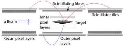
The Mu3e detector has to be capable of running at these very high muon rates and suppressing background from both the allowed radiative decay with internal conversion [6] and accidental combinations of electrons and positrons from different muon decays. This requires an excellent momentum, vertex and timing resolution of the detector. The low momenta of the decay particles make multiple Coulomb scattering the dominating effect deteriorating the momentum resolution, which can be counteracted by minimizing the detector material and using an optimized tracking detector geometry. A schematic view of the detector is shown in Figure 1. Extremely thin tracking layers consisting of thick HV-MAPS [7, 8, 9] mounted on polyimide-aluminium flex-prints [10] and cooled by gaseous helium are used [11]. The HV-MAPS for Mu3e, the MuPix ASICs [12, 13, 14, 15, 16, 17], perform on-sensor digitization and zero-suppression and send out hit data via up to three Low-Voltage Differential Signalling (LVDS) links. Combinatorial background can be further suppressed by precise timing measurements, which are provided by scintillating fibres (SciFi, [18]) and tiles [19], read out by Silicon Photomultipliers (SiPMs). The SiPM signals are digitized using the custom MuTRiG ASIC [20, 21], which also provides a LVDS output. The high granularity of the detector combined with the large particle rates produces an enormous amount of data; the Data Acquisition (DAQ) system has to deal with roughly at muons per second. Table I lists the bandwidth requirements estimated from a detailed, Geant4-based [22] simulation of the Mu3e detector.
| Sub-detector | Maximum hit rate | Maximum bandwidth needed | Number of | Total expected |
| per front-end board | per front-end board | front-end boards | data rate | |
| MHz | Gbit/s | Gbit/s | ||
| Pixels | 58 | 4.6 | 88 | 56 |
| Fibres | 28 | 2.3 | 12 | 28 |
| Tiles | 15 | 1.2 | 14 | 17 |
| Estimated from the detector simulation. For the fibre detector, clustering in the front-end FPGA is performed. For the bandwidth, protocol efficiency and 8b/10b encoding are assumed. | ||||
Mu3e uses a triggerless, streaming DAQ that employs a network of FPGAs and fast optical links [23] to transport all data out of the detector volume to a small farm of PCs equipped with powerful Graphics Processing Units (GPUs) for particle track and vertex reconstruction. The low momentum of the decay particles combined with the strong magnetic field leads to strongly curved tracks. Particles can thus produce hits in physically distant parts of the detector; see Figure 1. The resulting very non-local track finding problem requires that the data from the complete detector are available on every farm node. The readout network thus rearranges the data such that the farm nodes see the complete detector data of different time slices.
The Maximum Integrated Data Acquisition System (MIDAS, [24, 25]) is used as the software framework for the Mu3e DAQ. All DAQ PCs run so-called MIDAS Front-ends interacting with the DAQ hardware either via PCIExpress (PCIe) or Ethernet.
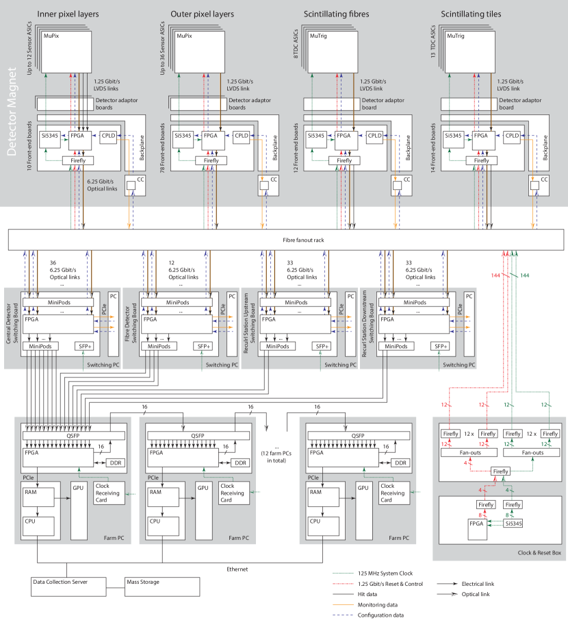
The architecture of the Mu3e DAQ is shown in Figure 2. In this paper, we will discuss the path of data through the system and introduce the hardware used.
II The DAQ system
II-A Front-end ASICs
The phase I Mu3e experiment will be built from 2844 MuPix pixel sensors complemented by scintillating fibres with 3072 SiPM readout channels and 5824 scintillating tiles. The pixel sensors as well as the 278 MuTRiG ASICs reading out the scintillating detectors send zero-suppressed hit data over 8b/10b encoded [26] LVDS links.
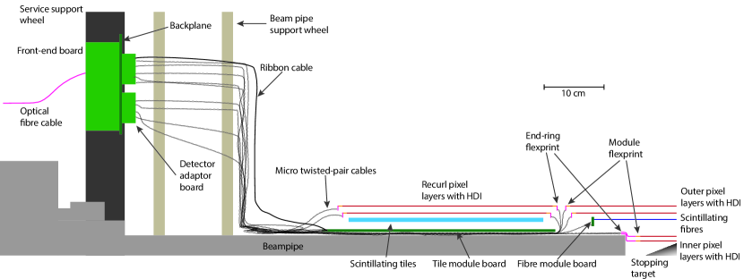
The detector concept with a particle tracking volume outside of the detector tube and all signal lines routed inside (together with channels for the gaseous helium cooling system, copper bars for power and ground as well as the beam pipe) lead to very tight space constraints for signal cabling; see Figure 3 for an overview. In the case of the pixel detector, the data first have to be transported out of the active tracking region, implying that material has to be minimized in order to reduce multiple Coulomb scattering of decay particles. The signals are thus routed over thin aluminium-polyimide high-density interconnects [11] out of the active region. Flexible PCBs connected by interposers are then used for transferring them to micro twisted-pair cables leading to the Service Support Wheels (SSWs), located close to the ends of the bore of the long solenoid magnet. For the inner pixel layers, three links per pixel sensor, each capable of transmitting about are connected, whereas in the outer pixel layers, only one link is connected.
For the fibre detector, one 128 channel SiPM array is connected to one SciFi module board with four MuTRiG ASICs. These module boards are then connected via micro twisted-pair cables to the SSW. In case of the tile detector, one MuTRiG chip reads 32 individual SiPMs and thirteen MuTRiGs are collected on one tile module board, which is then connected to the SSW using a ribbon cable.
II-B Front-end board
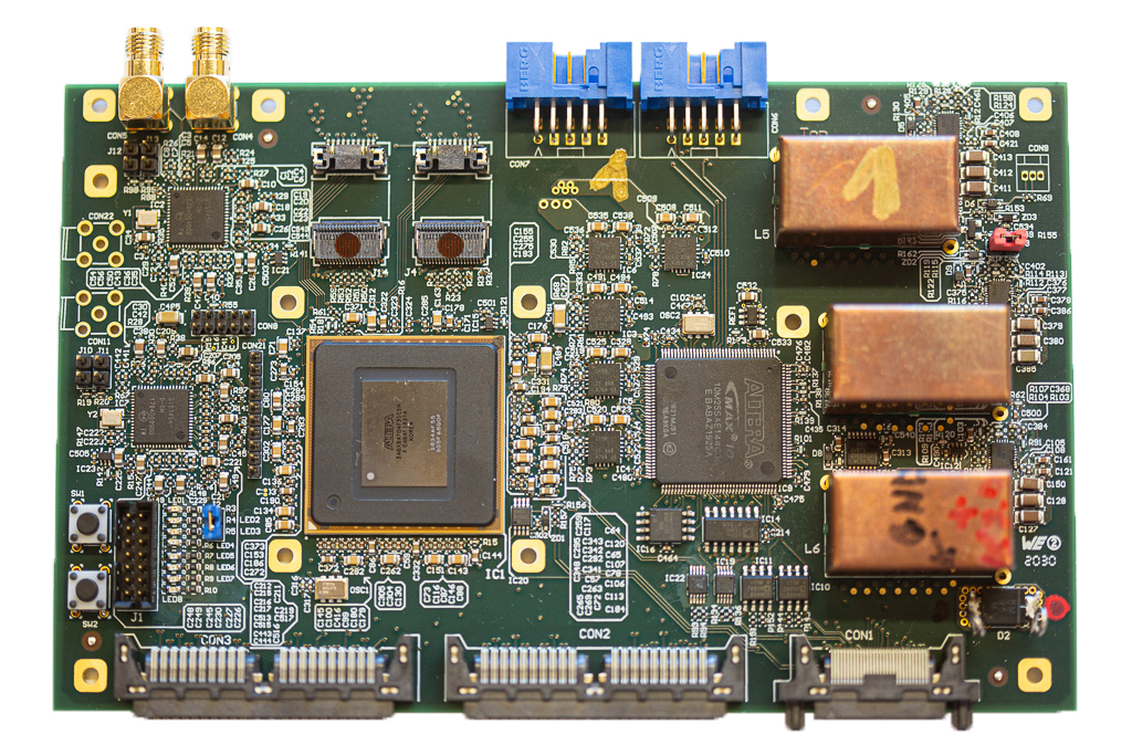
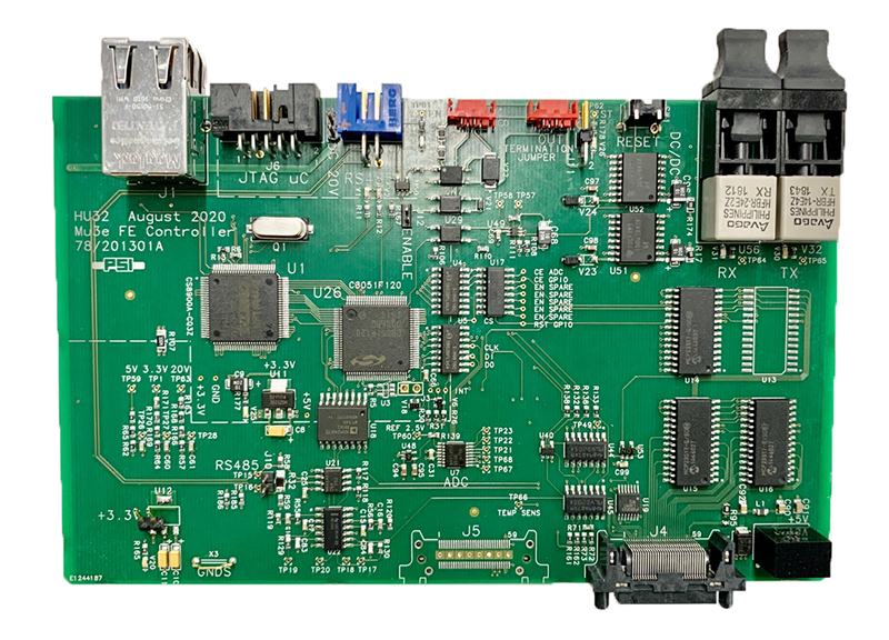
A total of 114 Front-End Boards (see Figure 4) collect the sensor data, perform data processing on an FPGA and then send the data out of the magnet volume using optical links. We decided to use a common front-end board for all sub-detectors and do the detector specific signal routing on a detector adaptor board. The euro-card-sized boards sit in quarter-circular crates on the SSW. A backplane links up to 16 front-end boards to a crate controller card and connects up to two detector adaptor boards to a front-end board. The crate controller card (see Figure 5) uses a SiLabs C8051F120 micro-controller running a bare-metal C control program. On one side it connects to each front-end board via the backplane, and on the other side it connects to the experiment’s control network using the MIDAS Slow Control Bus (MSCB, [27]) via either a standard Ethernet network (for tests outside the magnet) or an optical link. Boards can individually be power cycled in case of problems or firmware updates. A dedicated stand-by power allows temperature measurements in all front-end boards even if their power is off, which might be useful if problems with the cooling system occur.
Data processing on the front-end board is performed by an Intel Arria V A7 FPGA: The incoming data are 8b/10b decoded, and hits are separated from monitoring information. The links are continuously monitored by detecting 8b/10b encoding and parity errors as well as deviations from the data protocol.
For the pixel detector, a time-walk correction based on the measured time over threshold is applied to the hit time stamps. The hits are then time sorted using insertion into memory at addresses determined by the hit time stamp [28]. A list of the hits from each ASIC and each time stamp is generated. These lists are then processed into a single memory read sequence. Executing this read sequence produces a single, fully time-sorted output stream containing the data from up to 36 input links.
Due to the way the fibre ribbons are matched to the SiPM arrays, particles passing the detector almost always trigger more than one SiPM channel. The hits of the fibre detector are therefore clustered in time and space on the FPGA. Suppression of single hit clusters allows to reduce the bandwidth consumed by dark counts considerably, which would otherwise dominate over particle signals, especially after irradiation of the SiPMs.
The resulting data streams are interleaved with monitoring information and sent off-board using a Samtec Firefly ECUO-B04 optical transceiver.
The Firefly transceiver offers four inputs and four outputs; one of the inputs is used to receive the system clock. Two Silicon Labs Si5345 jitter cleaners and clock multipliers receive the clock and produce five clocks for the detector ASICs and eleven clocks for the FPGAs. A second input is used for resets and run state transitions; here we use a , 8b/10b encoded data stream called reset stream, where the datagrams are encoding different transitions. Special care has to be taken in the firmware to ensure that resets occur on a specific clock edge all across the system [29]. A third input is used for control and configuration information, e.g. the threshold tune values of all the connected pixels. This link runs at . The remaining incoming link serves as a spare clock input, three of the outgoing links provide spare bandwidth for upgrades, as does a second firefly socket that is left unequipped per default.
The Arria V is configured and controlled from an Intel MAX 10 FPGA (capable of configuring itself from built in flash memory). On power-up the MAX 10 reads the Arria configuration data from an external quad-SPI flash memory. The flash memory can be written by the MAX 10 using data received from a JTAG interface (only available with open detector) or from the crate controller and the backplane (slow) or from the configuration optical link, via the Arria and an inter-FPGA SPI interface (fast, but requiring programmed Arria). The MAX 10 also offers an ADC with a multiplexer, which is used to monitor the supply voltages on the board and to read several strategically placed analogue temperature sensors.
The front-end board is powered with from the backplane. Three switching DC/DC converters produce the , and needed on the board; the other voltages required are generated using linear regulators. As the boards are operated inside a solenoid, the inductors for the switching converters cannot have ferrite cores; we employ air-core solenoids inside copper shielding boxes [30, 31]. The overall power consumption is below . The boards are cooled with custom aluminium plates in thermal contact with the main heat-producing components. A heat-pipe connects the aluminium plate with the water-cooled SSW crate.
II-C Switching board
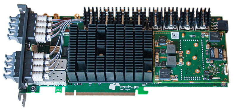
After about of multi-mode optical fibre, the optical cables from the front-end boards reach the Mu3e counting house, where a large fibre patch panel separates the clock and reset fibres from the control and data fibres. The latter are routed to four PCIe40 switching boards; see Figure 6. These cards, developed in Marseille for the LHCb and ALICE upgrades [32], provide 48 high-speed optical inputs and outputs using a total of eight Avago MiniPods. An Intel Arria 10 FPGA provides two generation 3, 8-lane PCIe interfaces.
On the switching board FPGA, the data streams from up to 34 front-end boards are time-aligned and merged. For the fibre detector, coincidences between the signals from the two fibre ends are formed to further suppress SiPM dark counts. The resulting data streams for all detectors are then forwarded to the filter farm using optical links. Matching the bandwidth requirements (see Table I), the central pixel detector uses eight links, the fibre detector uses four links and the forward and backward combined pixel and tile detector stations use two links each. We use custom protocols on all fibre links tailored to make maximum use of the bandwidth given that we have just three hit types, all with well-defined sizes and formats.
For each data link from the front-end boards, there is a control link going in the opposite direction. This is used for configuration data (such as the threshold tune values for more than 180 million pixels) and to request monitoring information such as temperature values from the front-end boards. The switching board FPGA is also used to extract information such as hit maps and other histograms from the incoming data streams, which is made available to the MIDAS DAQ via the PCIe interfaces.
All the Arria 10 FPGAs in the experiment feature generation 3, 8-lane PCIe interfaces with common firmware, Linux kernel driver and software. The PCIe firmware provides four Bus-Addressable Register (BAR) areas. The first BAR provides 64 registers writeable from the FPGA, the second BAR 64 registers writeable from the PC, the third and fourth BARs are memories, one writeable from the FPGA, one from the PC. This is complemented by a direct memory access (DMA) engine for fast data transfers to the PC main memory. The DMA buffer on the PC is treated as a large ring buffer. Signalling to the PC occurs without interrupts by performing DMA to a separate control memory area containing pointers to the last written blocks [33]. In tests of our DMA firmware, we can sustain of user data transfers [34].
II-D Filter farm
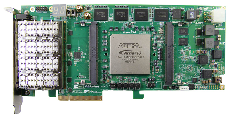
The sixteen links from the switching boards are routed to the Mu3e filter farm, which consists of twelve PCs in a daisy chain configuration. Each PC is equipped with a receiving board. Here we use the commercial DE5aNET board [35] produced by Terasic Inc. It features an Intel Arria 10 FPGA connected to four QSFP quad-optical transceivers and two banks of DDR4111Earlier versions feature DDR3 memory. memory. It connects to the host PC using one 8-lane generation 3 PCIe interface.
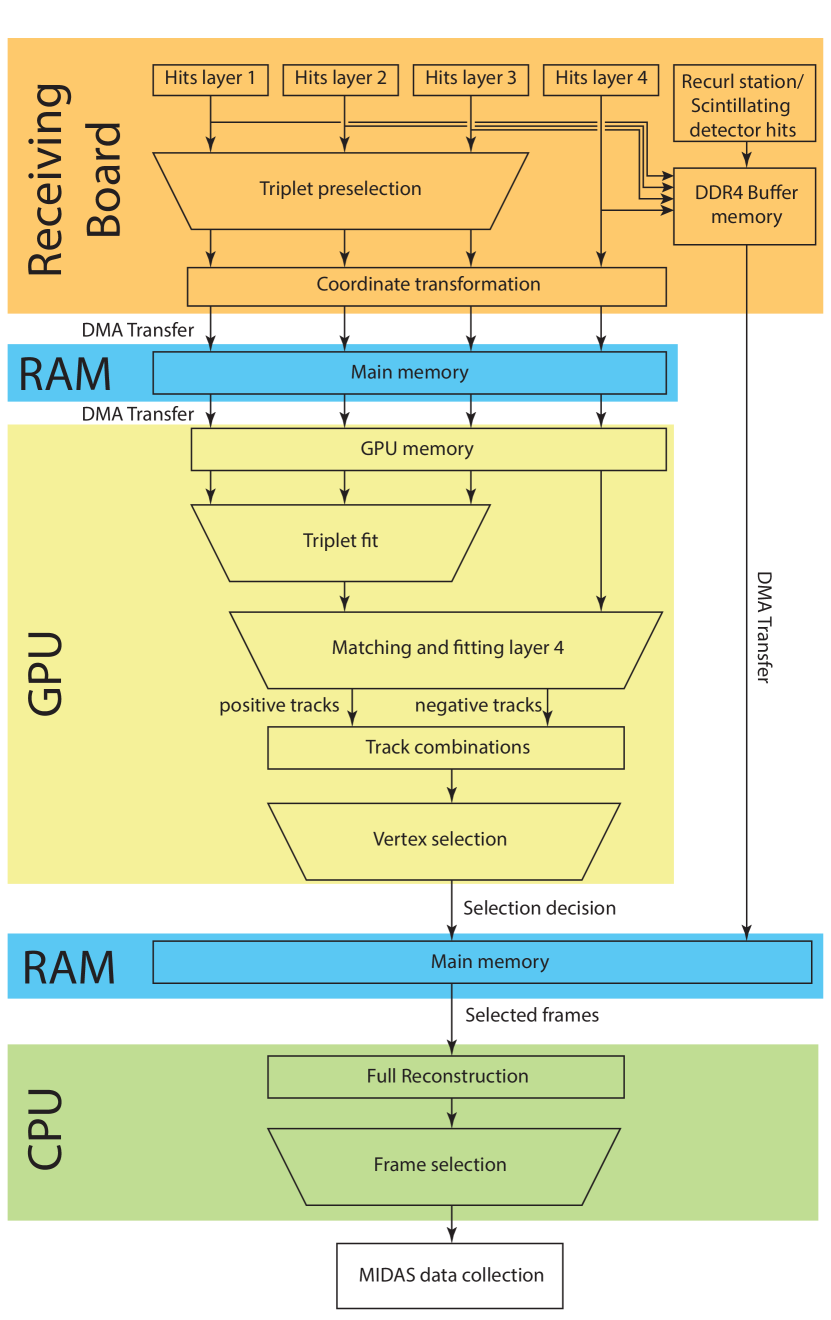
Figure 8 shows a schematic of the data flow in a single farm node. The data from the sixteen links are received, time aligned and buffered to the DDR4 memory. If the buffers are full, the data are forwarded to the next PC in the daisy chain, providing a simple form of load distribution without the need for a back-channel and back-pressure. The hits of the central pixel detector are extracted from the data stream, and a first geometrical selection is performed based on hits from the first three detector layers; only hit triplets compatible with stemming from a track originating in the target region are processed further. Using look-up memories, the hit coordinates are transformed from the sensor/column/row scheme to the global detector coordinate system (using three single-precision floating point numbers). The hits are then sent to the main memory of the host PC using DMA transfers. From the main memory, the hit data are then forwarded to a GPU222Due to the rapid developments of the GPU market at the time of writing in terms of both prices and performance, we will choose the exact model of GPU for production use as late as possible. Currently we aim for mass-market gaming cards.. On the GPU, a custom developed track fit treating multiple scattering as the only uncertainty [36] is performed on hits from the first three detector layers. If successful, the track is extrapolated to the fourth layer and if a matching hit is found, it is included in the fit, or otherwise the track is discarded. Lists of tracks with positive and negative charge assignments are created and a simple vertex fit based on circle intersections is performed for all combinations of two positive and one negative track (corresponding to the signal topology) [33]. If the three tracks are compatible with originating in a common vertex, the frame is tagged for readout. In this case the complete detector information for the frame is retrieved from the DDR4 buffer, passed to the main memory of the host PC and a full reconstruction [37] is performed. Signal candidate events are saved using the MIDAS event handling infrastructure to the PetaByte Archive operated jointly by PSI and the Swiss supercomputing centre CSCS. We aim for an output data rate of about to keep storage requirements manageable and affordable. If the selection criteria are relaxed, the DAQ system is easily capable of saturating the bandwidth of both local storage media or the outgoing Ethernet connection.
As the muon decays on the target have no particular time structure, the online reconstruction on the GPUs is performed in overlapping time frames333The size of the overlap will be determined once the exact time resolution of the production pixel sensor is known. of length in order to avoid an efficiency loss at the frame boundary. The frame size is chosen to cover at least of the pixel time resolution and has to be a multiple of the time stamp bin size.
The Mu3e detector is peculiar in as much as the reconstructed information (i.e. the helix parameters of a track represented as floating-point numbers) takes more space than the raw data. This, together with the high rates, precludes saving e.g. track kinematics for all events. What can however be done is the histogramming of such quantities on the GPUs. Given a good calibration of the online reconstruction, these histograms can be used in physics analyses, e.g. searches for two-body decays of the muon , where Mu3e has a very competitive sensitivity [28, 38, 39].
II-E Synchronisation
The Mu3e detector and DAQ are all synchronised to a master clock, and all other clocks, e.g. the clock for the MuTRiG TDC ASICs or the optical link clocks are derived from this master clock using Phase-Locked Loops (PLLs). In order to also determine a common starting point for time stamps, a common reset signal is distributed to all parts of the experiment. For this we employ the , 8b/10b encoded reset stream, which we can also use to signal state transitions such as run starts and stops.
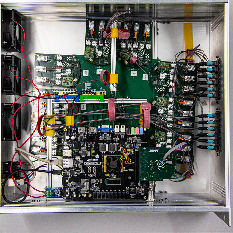
The reset and clock are generated and fanned-out in a single four unit 19 inch box, the clock and reset system; see Figure 9. The master clock is generated by a Silicon Labs SI5345 clock generation IC. The reset stream is generated using a gigabit transceiver on a commercial Digilent Genesys 2 board [40]. This board, featuring a Xilinx Kintex-7 FPGA, is also used to configure and monitor the clock and reset system. The modular system uses one mother- and eight daughter-boards equipped with ON-Semiconductor NB7L1008M differential eight-fold fan-out chips. Samtec Firefly transmitters are used to generate the 144 optical clock copies and the 144 optical reset stream copies. A jitter of less than between the different output clocks (after optical transmission and back-conversion to differential electrical signals) was measured, easily fulfilling the specification.
III Conclusion
We have presented the design and hardware implementation of the Mu3e data acquisition, a compact and cost effective system capable of dealing with rates in excess of . The fully streaming system employs a custom front-end board inside the detector magnet collecting the detector ASIC data and forwarding them optically to switching boards in the counting house, which also interface to the detector control and monitoring. A small filter farm employing FPGA receiving boards and consumer GPUs performs a full track reconstruction and selects events of interest. All components of the Mu3e DAQ are available and were successfully tested. The full system is expected to be set up a PSI and operational by the end of 2021.
References
- [1] G. Hernández-Tomé, G. López Castro, and P. Roig, “Flavor violating leptonic decays of and leptons in the Standard Model with massive neutrinos,” Eur. Phys. J. C, vol. 79, no. 1, p. 84, 2019, [Erratum: Eur. Phys. J. C 80, 438 (2020)].
- [2] P. Blackstone, M. Fael, and E. Passemar, “ at a rate of one out of tau decays?” Eur. Phys. J. C, vol. 80, no. 6, p. 506, 2020.
- [3] U. Bellgardt et al., “Search for the Decay ,” Nucl. Phys., vol. B299, p. 1, 1988.
- [4] A. Blondel et al., “Research Proposal for an Experiment to Search for the Decay ,” 2013, arXiv:1301.6113.
- [5] K. Arndt et al., “Technical design of the phase I Mu3e experiment,” 9 2020, submitted to Nucl. Instr. Meth. A.
- [6] G. Pruna, A. Signer, and Y. Ulrich, “Fully differential NLO predictions for the rare muon decay,” Phys. Lett. B, vol. 765, pp. 280–284, 2017.
- [7] I. Perić, “A novel monolithic pixelated particle detector implemented in high-voltage CMOS technology,” Nucl. Instr. Meth., vol. A582, pp. 876–885, 2007.
- [8] I. Perić et al., “High-voltage pixel detectors in commercial CMOS technologies for ATLAS, CLIC and Mu3e experiments,” Nucl. Instr. Meth., vol. A731, pp. 131–136, 2013.
- [9] ——, “Overview of HVCMOS pixel sensors,” JINST, vol. 10, no. 05, p. C05021, 2015.
- [10] N. Berger et al., “Ultra-low material pixel layers for the Mu3e experiment,” JINST, vol. 11, no. 12, p. C12006, 2016.
- [11] F. Meier Aeschbacher, M. Deflorin, and L. Noehte, “Mechanics, readout and cooling systems of the Mu3e experiment,” PoS, vol. Vertex2019, p. 041, 2020.
- [12] H. Augustin et al., “The MuPix high voltage monolithic active pixel sensor for the Mu3e experiment,” JINST, vol. 10, no. 03, p. C03044, 2015.
- [13] ——, “MuPix7 - A fast monolithic HV-CMOS pixel chip for Mu3e,” JINST, vol. 11, no. 11, p. C11029, 2016.
- [14] ——, “The MuPix System-on-Chip for the Mu3e Experiment,” Nucl. Instrum. Meth., vol. A845, pp. 194–198, 2017.
- [15] ——, “Efficiency and timing performance of the MuPix7 high-voltage monolithic active pixel sensor,” Nucl. Instr. Meth. A, vol. 902, p. 158, 2018.
- [16] ——, “MuPix8 — Large area monolithic HVCMOS pixel detector for the Mu3e experiment,” Nucl. Instrum. Meth. A, vol. 936, pp. 681–683, 2019.
- [17] ——, “Performance of the large scale HV-CMOS pixel sensor MuPix8,” JINST, vol. 14, no. 10, p. C10011, 2019.
- [18] S. Bravar, S. Corrodi, A. Damyanova, C. Grab, R. Gredig, A. Papa, and G. Rutar, “Scintillating fibre detector for the Mu3e experiment,” JINST, vol. 12, no. 07, p. C07011, 2017.
- [19] H. Klingenmeyer, Y. Munwes, K. Briggl, T. Zhong, H. Chen, W. Shen, and H.-C. Schultz-Coulon, “Measurements with the technical prototype for the Mu3e tile detector,” Nucl. Instrum. Meth. A, vol. 958, p. 162852, 2020.
- [20] H. Chen, K. Briggl, P. Eckert, T. Harion, Y. Munwes, W. Shen, V. Stankova, and H. C. Schultz-Coulon, “MuTRiG: a mixed signal Silicon Photomultiplier readout ASIC with high timing resolution and gigabit data link,” JINST, vol. 12, no. 01, p. C01043, 2017.
- [21] H. Chen, W. Shen, K. Briggl, V. Stankova, Y. Munwes, D. Schimansky, and H.-C. Schultz-Coulon, “Characterization Measurement Results of MuTRiG - A Silicon Photomultiplier Readout ASIC with High Timing Precision and High Event Rate Capability,” PoS, vol. TWEPP-17, p. 008, 2017.
- [22] S. Agostinelli et al., “GEANT4: A Simulation toolkit,” Nucl. Instrum. Meth., vol. A506, pp. 250–303, 2003.
- [23] S. Bachmann et al., “The proposed trigger-less TBit/s readout for the Mu3e experiment,” JINST, vol. 9, p. C01011, 2014.
- [24] S. Ritt, P. Amaudruz, and K. Olchanski, “The MIDAS data acquisition system,” Proc. IEEE 10th Real Time Conf., pp. 309–312, 1997.
- [25] ——, “Maximum Integration Data Acquisition System,” 2001. [Online]. Available: https://midas.triumf.ca/
- [26] A. X. Widmer and P. A. Franaszek, “A DC-Balanced, Partitioned-Block, 8B/10B Transmission Code,” IBM Journal of Research and Development, vol. 27, p. 440, 1983.
- [27] S. Ritt and R. Schmidt, “MSCB (MIDAS Slow Control Bus),” 2001. [Online]. Available: https://elog.psi.ch/mscb/
- [28] A.-K. Perrevoort, “Sensitivity Studies on New Physics in the Mu3e Experiment and Development of Firmware for the Front-End of the Mu3e Pixel Detector,” PhD Thesis, Heidelberg University, 2018.
- [29] M. Müller, “A Control System for the Mu3e Data Acquisition,” Master Thesis, Mainz University, 2019.
- [30] M. Hesping, “Air Coils for Powering the Mu3e Experiment,” Bachelor Thesis, Mainz University, 2019.
- [31] S. Gagneur, “Developement of a DC-DC Converter for the Mu3e Detector,” Master Thesis, Mainz University, 2020.
- [32] J. P. Cachemiche, P. Y. Duval, F. Hachon, R. Le Gac, and F. Réthoré, “The PCIe-based readout system for the LHCb experiment,” JINST, vol. 11, no. 02, p. P02013, 2016.
- [33] D. vom Bruch, “Pixel Sensor Evaluation and Online Event Selection for the Mu3e Experiment,” Ph.D. dissertation, Heidelberg University, 2017.
- [34] M. Köppel, “Data Flow in the Mu3e Filter Farm,” Master Thesis, Mainz University, 2019.
- [35] “DE5a-NET FPGA Development Kit User Manual,” Terasic Inc, Tech. Rep., 2019.
- [36] N. Berger, M. Kiehn, A. Kozlinskiy, and A. Schöning, “A New Three-Dimensional Track Fit with Multiple Scattering,” Nucl. Instrum. Meth., vol. A844, p. 135, 2017.
- [37] A. Kozlinskiy, “Track reconstruction for the Mu3e experiment based on a novel Multiple Scattering fit,” EPJ Web Conf., vol. 150, p. 00005, 2017.
- [38] A.-K. Perrevoort, “The Rare and Forbidden: Testing Physics Beyond the Standard Model with Mu3e,” SciPost Phys. Proc., vol. 1, p. 052, 2019.
- [39] L. Calibbi, D. Redigolo, R. Ziegler, and J. Zupan, “Looking forward to Lepton-flavor-violating ALPs,” 6 2020.
- [40] “The Digilent Genesys 2 Kintex-7 FPGA development board.” [Online]. Available: https://reference.digilentinc.com/reference/programmable-logic/genesys-2/