Performance of the Unified Readout System of Belle II
Abstract
The Belle II experiment at the SuperKEKB collider at KEK, Tsukuba, Japan has successfully started taking data with the full detector in March 2019. Belle II is a luminosity frontier experiment of the new generation to search for physics beyond the Standard Model of elementary particles, from precision measurements of a huge number of and charm mesons and tau leptons. In order to read out the events at a high rate from the seven subdetectors of Belle II, we adopt a highly unified readout system, including a unified trigger timing distribution system (TTD), a unified high speed data link system (Belle2link), and a common backend system to receive Belle2link data. Each subdetector frontend readout system has a field-programmable gate array (FPGA) in which unified firmware components of the TTD receiver and Belle2link transmitter are embedded. The system is designed for data taking at a trigger rate up to 30 kHz with a dead-time fraction of about 1% in the frontend readout system. The trigger rate is still much lower than our design. However, the background level is already high due to the initial vacuum condition and other accelerator parameters, and it is the most limiting factor of the accelerator and detector operation. Hence the occupancy and radiation effects to the frontend electronics are rather severe, and they cause various kind of instabilities. We present the performance of the system, including the achieved trigger rate, dead-time fraction, stability, and discuss the experience gained during the operation.
Index Terms:
Availability, Centralized control, Data acquisition, Data transfer, High energy physics, Radiation effects, System integration, SynchronizationI Introduction
Belle II experiment [1] at the SuperKEKB collider [2] at KEK, Tsukuba, Japan has successfully started the data taking to search for physics beyond the Standard Model of elementary particles. The goal of the Belle II experiment is to collect an unprecedented 50 ab-1 integrated luminosity, mostly at the resonance, to study and search for a wide range of meson decays, charm meson decays, lepton decays, and hypothetical particles such as those expected from the dark sector. The design instantaneous luminosity is cm-2s-1, 40 times higher than the highest luminosity achieved by its predecessor, KEKB. Thanks to the clean environment of the collision, the events are triggered with a single level (level-1) trigger system with a trigger efficiency greater than 99% for most of the meson decay modes. The level-1 trigger rate is designed to be up to 30 kHz, which includes about 1 kHz each of -meson-pair, charm-pair, and -lepton-pair events.
The Belle II detector consists of seven subdetectors: a pixel detector (PXD) and a silicon-strip vertex detector (SVD) for vertex reconstruction, a central drift chamber (CDC) for charged track reconstruction, a time-of-propagation counter (TOP) and an aerogel ring imaging Cherenkov detector (ARICH) for charged hadron identification, an electromagnetic calorimeter (ECL) for photon detection and electron identification, and a and muon detector (KLM) in the return yoke of the 1.5 T solenoid coil. The event is read out upon each level-1 trigger decision based mostly on CDC and ECL trigger information, which is given within a latency of about 5 s. All the detector data are digitized inside or nearby the detector, and collected by the data acquisition system.
The first physics run was in 2018 with the Belle II detector without the vertex detectors, under the so-called phase 2 operation. The main purposes were the commissioning of the accelerator, evaluation of the background condition for the vertex detectors, and initial physics programs with a low-multiplicity trigger condition and with no requirement on the precise vertex information. The main physics program, so-called phase 3, has successfully started in 2019 with the full Belle II detector. Although the luminosity is still far below the design, it reached the peak of , already exceeding the previous record established by KEKB. Belle II has collected of data, with an overall efficiency of about 84%, as discussed later.
In this paper, we first briefly describe the unified readout system of Belle II, and then the performance of the system and various problems we experienced in the first two years of operation.
II Unified Readout System
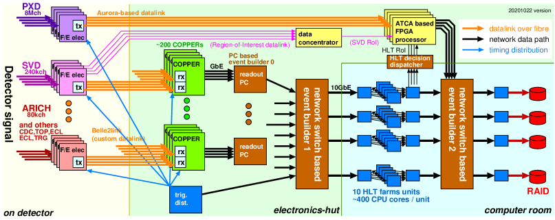
In order to read out the events from the seven subdetectors, we adopt a highly unified readout system [3][4], including a unified trigger timing distribution (TTD) system for the entire Belle II detector, a unified high speed data link system called Belle2link, which is used by all subdetectors except PXD, and a common backend system called COPPER to receive the Belle2link data. Every subdetector frontend electronics (FEE) device has an FPGA in which the unified firmware components of TTD receiver and Belle2link transmitter are embedded.
The system aims for taking data at 30 kHz trigger rate with a dead-time fraction of about 1% from the frontend readout system. The read-out data are sent to the backend data acquisition system comprised of the event builder, high level trigger and storage system. The schematic view of the Belle data acquisition system is given in Fig. 1.
II-A Unified Trigger Timing Distribution
The TTD system [5] consists of a network of the frontend-timing-switch (FTSW) modules in a tree structure, to distribute the system clock, level-l trigger timing, and other information for fast control to a large number of FEE boards and COPPER modules, and to collect their status. The system clock of 127 MHz is generated from the 509 MHz radio frequency (RF) of SuperKEKB, and is directly distributed using a dedicated line. The remaining signals are embedded in a bidirectional serial link of 254 Mbps using a custom protocol called b2tt. These signals are transmitted as low voltage differential signaling (LVDS) signals over a low-cost category-7 network cable for most of the short distance connections, or over two pairs of multimode fibers for the long distance connections between the stations on the detector and the electronics-hut where the center of the TTD system resides.
The FTSW module [5] is a multi-purpose double-width 6U-height VMEbus [6] module equipped with a Xilinx [7] Virtex-5 FPGA and 24 RJ-45 connectors. Four of these connectors have dedicated purposes: one for the connection to uplink, one for programming of the FPGA of the FTSW using JTAG [8], one for Ethernet (unused), and one for multipurpose LVDS input or output; and remaining 20 connectors are used for distribution. The bottom 4 or 8 distribution RJ-45 connectors can be replaced with an FMC daughter card with 2- or 8-port SFP optical transceivers, to receive or distribute the b2tt serial-link signals. Up to 4 stages of cascaded connections of FTSW modules are used to deliver the TTD signal to more than 1,000 destinations of FEE boards and other systems as shown in Fig. 2.
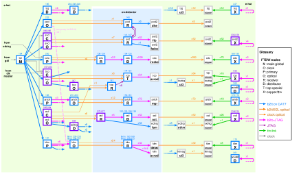
The FTSW module is also used to deliver the JTAG signals to the frontend boards, first encoded in the b2tt protocol and delivered to the last step of the FTSW tree, and then transmitted as LVDS level signals to the FEE over another category-7 cable. Therefore, a typical FTSW module on the detector is receiving the b2tt serial link over 2 pairs of fibers and connected with 8 FEE boards for timing distribution and JTAG programming.
The TTD system distributes the level-1 trigger signal with the event number, timestamp and trigger type. The timestamp is a unique and monotonically incremented 59-bit value for every event, and it is saved in the data to be used later to detect event mismatch and data errors at various stages of the readout chain. The trigger type is used to dynamically change the readout operation of FEE depending on the trigger source. The trigger interval is controlled by a programmable interval counter and an emulation logic of the SVD FEE to avoid the overflow in the SVD FEE, which has the most timing-critical condition among subdetectors. In addition, busy signals are collected to temporarily pause the trigger distribution as the back pressure from the backend data transport and some of the FEE systems.
At the same time, the TTD tree is used to collect and summarize the status of the readout system, including error information, number of processed events, and status of the SEU mitigation (see section IV-A). Each connection can be masked or reset remotely, to avoid spurious information from unused or malfunctioning links. In addition to the FEE, the TTD system also distributes various fast timing information to subdetector and global trigger processors, luminosity counters, and beam background monitors.
II-B Unified Data Link — Belle2link
The Belle2link is a bi-directional custom high-speed serial link protocol to collect the data read out at the FEE [9]. It uses the 8b10b encoded high speed serial link function of the Xilinx FPGA. The raw bit rate is 2.54 Gbps, driven by the system clock, but the payload bandwidth is limited to about 1 Gbps at the FEE, mainly because the bandwidth is limited by the COPPER backend interface design and because there is no back pressure from the COPPER to the FEE for simplicity.
The receiver of the Belle2link is a single-channel optical receiver card called HSLB [9] equipped with a Xilinx Virtex-5 FPGA. Up to 4 HSLB cards are mounted on a COPPER module, which is a 9U-height VMEbus board. The COPPER module is driven by a processor card running Linux operating system on an Intel x86 processor. The COPPER module is a multi-purpose platform, which is also used by other experiments with different daughter cards instead of the HSLB.
The event fragment data sent from the FEE is checked for errors, and then copied to the FIFO buffer of the COPPER. The COPPER module then combines the event fragments and makes a direct memory access (DMA) transfer to the processor. The processor is used to make a minimal formatting and send the data to the next stage through a Gigabit Ethernet connection.
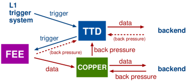
The COPPER board also is equipped with a trigger card for the connection to the TTD system. A programmable threshold is set to the FIFO buffer, and when the data exceeds the threshold, a back pressure is sent to the TTD system. The entire path of the trigger distribution, data collection, and back pressure is illustrated in Fig. 3.
The HSLB card also serves as interface to the FEE for read and write access to the 32-bit registers mapped onto a 16-bit address space. These registers are used to configure individual boards, such as setting the threshold or parameters that are needed for feature extraction from the read-out signal waveform, and reading the individual status of the FEE boards, such as the voltage of the supplied power or temperature of the FPGA.
II-C Subdetector Frontend Electronics
Although the TTD and Belle2link are common, the requirements and hence the hardware designs for the FEE boards differ among subdetectors. The simplest example is the CDC FEE board, which performs 48-channel preamplification, shaping and analog-to-digital conversion at a 31 MHz sampling cycle on the board, and time-to-digital conversion with a 1 ns least-significant-bit realized inside a Xilinx Virtex-5 FPGA. Other subdetectors require additional preprocessing steps, typically using an external analog-to-digital conversion circuit and a digital logic built in another FPGA. The most complex FEE is the one for TOP [10], which is built upon the Xilinx ZYNQ system-on-chip device with a Xilinx 7-series FPGA core for timing-critical logic and an Arm processor core for pipelined data processing. All subdetector frontend electronics are based on one of the Xilinx FPGA devices (Virtex-5, Spartan-6, Virtex-6, Kintex-7 or ZYNQ), with the exception of the flash-ADC controller board of SVD with the Stratix IV FPGA of Intel (Altera) [11].
II-D PXD and Backend
The data read out by the COPPER are collected and built into a raw event without the PXD data. The raw events are fed into the high level trigger (HLT) computing nodes, where the full event reconstruction is made to filter the events by up to a factor of 5. The HLT consists of multiple streams, each of which is an independent parallel processing block of computing nodes and dedicated input and output nodes. The number of HLT streams has been and will be increased in a staged way; HLT has been operated with 9 streams until summer 2020, and the stream 10 was added during summer shutdown.
The PXD data is not combined at this stage for two reasons. First, the data size, which is an order of magnitude larger than the sum of the rest, is beyond the limited bandwidth of the COPPER based unified readout system. Second, PXD information does not contribute to the HLT event filtering. Contrary, we use the reconstructed charged tracks at HLT to reduce the PXD data by an order of magnitude by only saving the region-of-interest subset, and make the final event building before saving the data into a storage device.
III Operation and Performance
The phase 3 operation of Belle II has started in March 2019, which is the final phase of the commissioning with all subdetectors and accelerator components. In 2019, it continued until July, and then after a summer break, resumed from October till December. The run in 2020 started in February and continued until July, and resumed in October to end in December.
III-A Operating Conditions
SuperKEKB and Belle II are nominally operated to continuously accumulate physics data, except for the scheduled half-day accelerator maintenance every 2 weeks. However, the current priority is in improving the peak luminosity rather than maximizing the integrated luminosity. Until summer 2020, day time of weekdays were usually devoted to the accelerator studies, and night time and weekend were used for physics data taking.
In the current operation, the beam current is limited to keep the beam background condition below the limit on the integrated dose to the photon detector of TOP. As a result, the trigger rate is still far below the design. Typical level-1 trigger rate around the end of the latest run period was around 4 kHz, whereas the design trigger rate of the system at the full luminosity is 30 kHz.
The time for accelerator studies are used to operate the data acquisition system with 30kHz dummy random triggers with intervals of a pseudo Poisson distribution. Since high voltage is not applied to the subdetectors, threshold is lowered for CDC to generate data with a reasonable occupancy. This dummy trigger operation has been useful to keep updating the firmware and software to improve the performance and stability.
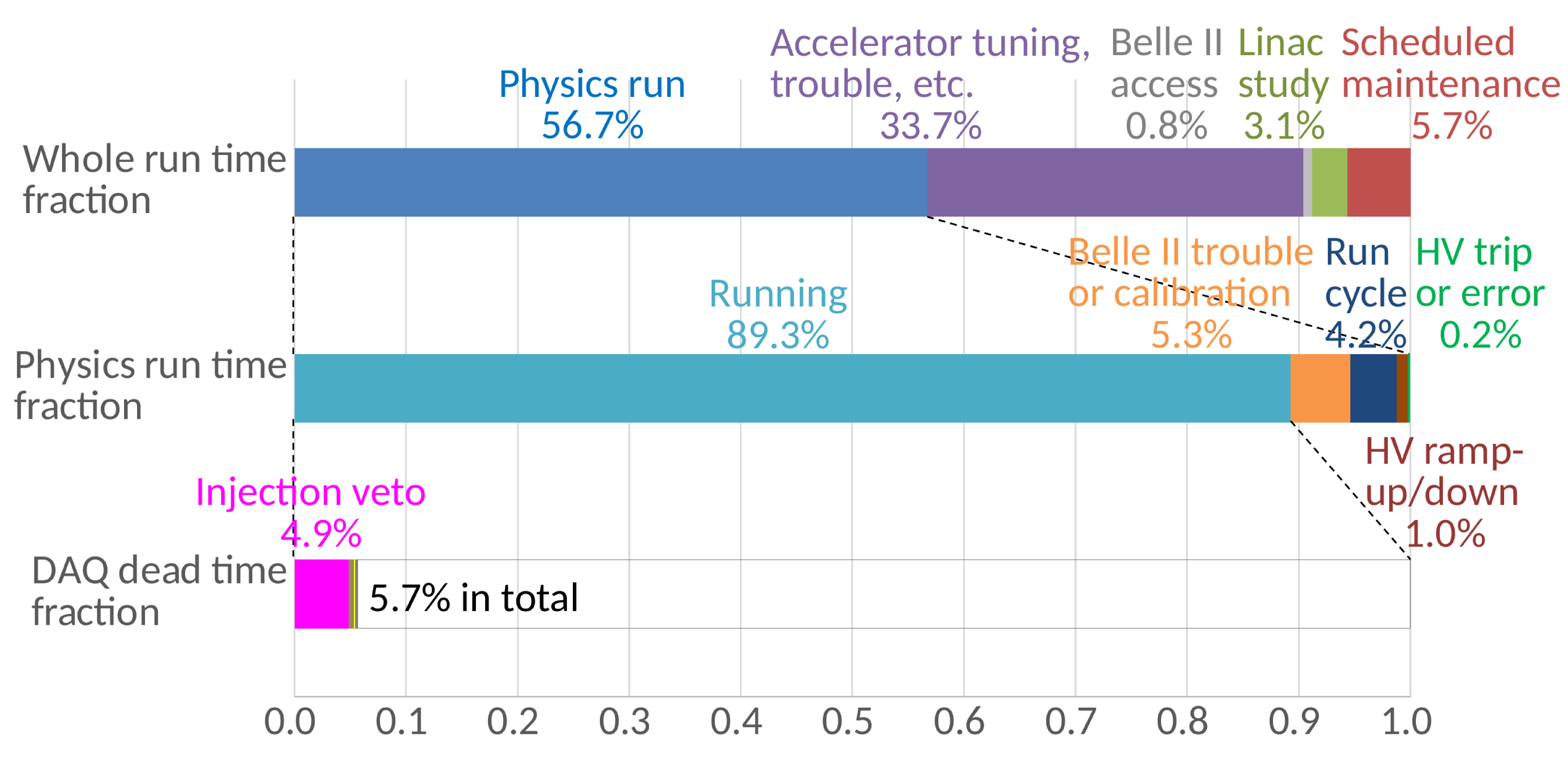
A summary of the operation and dead-time fraction in 2020 is given in Fig. 4, with an overall efficiency of 84.2%.
III-B Dead-time Fraction
The largest dead-time fraction during the stable operation comes from the veto window after the beam injection. In the continuous injection mode, the linac injects the beam to the main ring during the run to keep the beam current and other accelerator conditions constant. The beam injection occurs at a rate of 25 Hz at most. Each beam injection heavily disturbs the succeeding stored bunches near the injected bunch, and it also disturbs the stored bunches in the entire ring to some extent. In order to reduce the spurious triggers due to the disturbed bunches, the level-1 trigger is vetoed for all the bunches for a short period right after the injection, and for the bunches near the injection for a longer period. The veto length is tuned to minimize the dead-time fraction, which is about 5%.
The second major dead time comes from the run restart cycle, which typically takes about 2.5 minutes, but may take longer depending on the situation. We pose an 8-hour limit on the run length, but most of the runs are stopped much earlier by the loss of the beam or by an error in the data acquisition.
The dead-time fraction from the data acquisition system is less than 1%. Two dominant contributions come from the trigger throttle and slow-down of the readout software somewhere in the chain, e.g. caused by a flood of log messages when partially broken data are detected. Otherwise the dead-time fraction due to the data acquisition system itself is negligibly small.
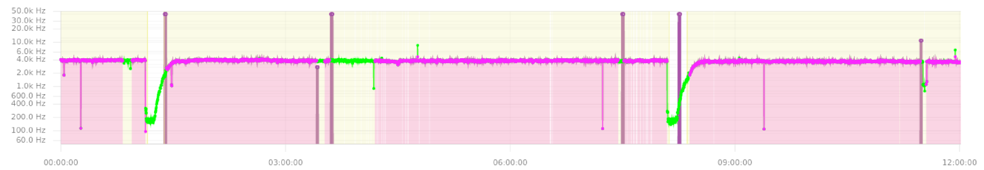
The trigger rate is still much lower than our design, but the background level is close to the highest level that detector can endure, as it is the largest limiting factor of the accelerator and detector operation. Hence the occupancy and the radiation effects to the frontend electronics are rather severe, causing various kind of instabilities. Fig. 5 shows an example of the trigger rate of about 4 kHz with several beam losses and recovery periods from data acquisition errors in a half day. Some of the data acquisition errors are due to immaturity of the firmware which has been diligently improved as the commissioning went on, while some are due to unstable hardware modules or connections which were replaced or fixed when it was possible.
III-C Readout Latency
We measure the latency of the data processing inside FEE as a part of the unified readout system, by including the timestamp of the start of the data transfer into the data header itself. This can be then compared with the timestamp of the trigger in the data stream in an offline analysis.
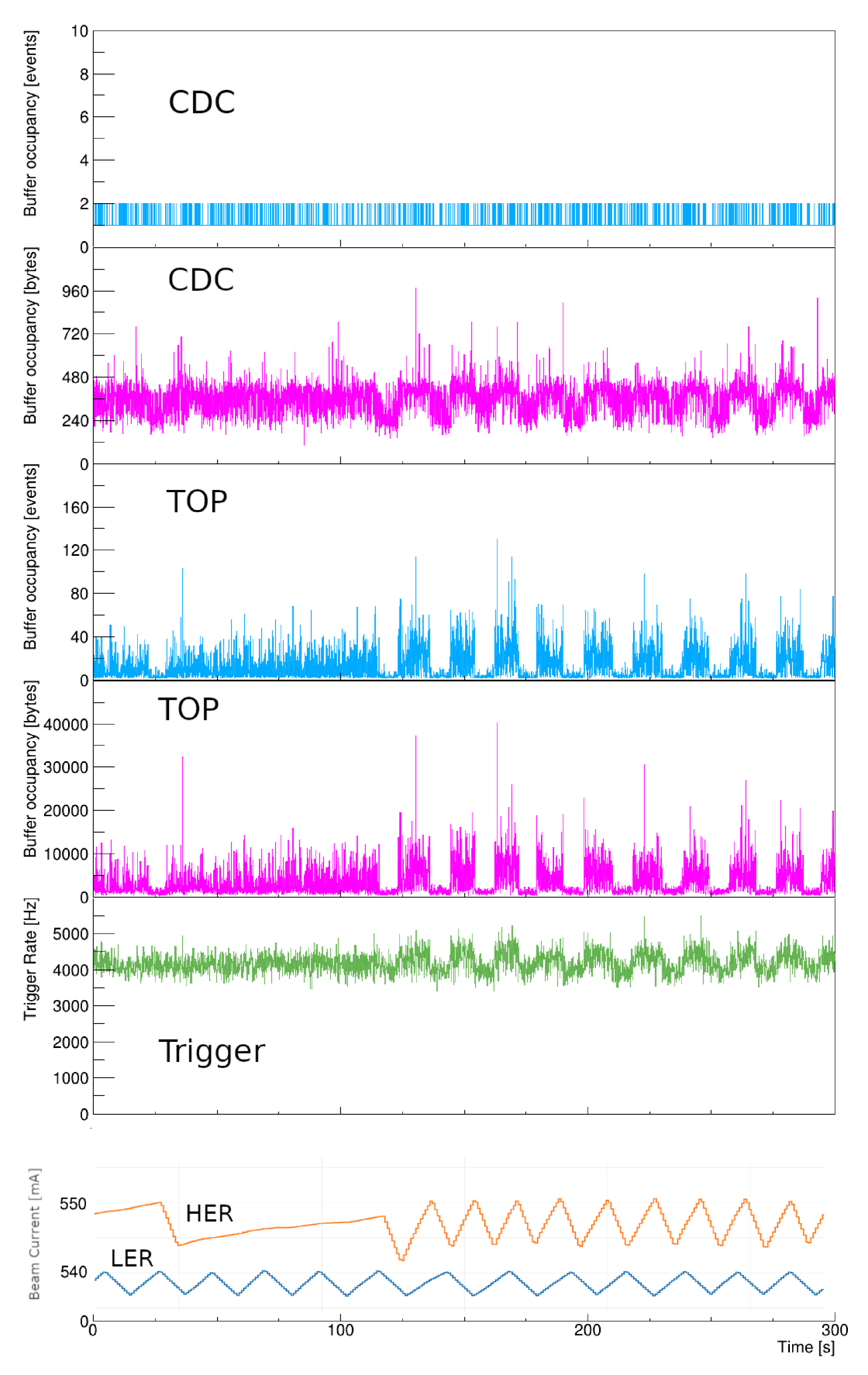
Fig. 6 shows the estimated buffer occupancy at the COPPER using this data latency, assuming the the buffer is swiftly read out at the ideal bandwidth of the COPPER board. The event fragment stays inside the FIFO buffer until all data of four links are aligned. Therefore the occupancy illustrates the typical size of event fragments and variation of the processing time in the FEE.
We find the CDC data latency to be the smallest and almost uniform, thanks to the single-board FEE configuration. We also find the TOP data latency is the largest and least uniform, as a result of software data processing in the Arm core of the FEE.
We also use this information to extrapolate to the 30 kHz design trigger rate to confirm that the COPPER buffer will not overflow.
IV Problems, Errors and Solutions
As already described, various problems and errors in the data acquisition system have been making a large contribution to the inefficiency of data taking. Most of the errors are understood and improved in 2020 with respect to the previous year, and will be further improved in coming runs. Here we classify the problems and errors into four categories: single event upset (SEU), link errors, hardware failures and other problems.
IV-A Single Event Upset (SEU)
The FEE boards of CDC, TOP and ARICH are inside the detector and are expected to suffer from gamma rays and neutrons. According to the previous studies [12], the most affected parts of a typical FEE board are the optical transceiver, which is permanently damaged by a large dose of gamma rays, and the FPGA, whose configuration or data memory bit is flipped by SEU caused by neutrons. The optical transceiver we adopted survived a 10-year equivalent integrated dose of gamma-rays in an irradiation test, while other typical transceivers we tested stopped working at a much smaller integrated dose.
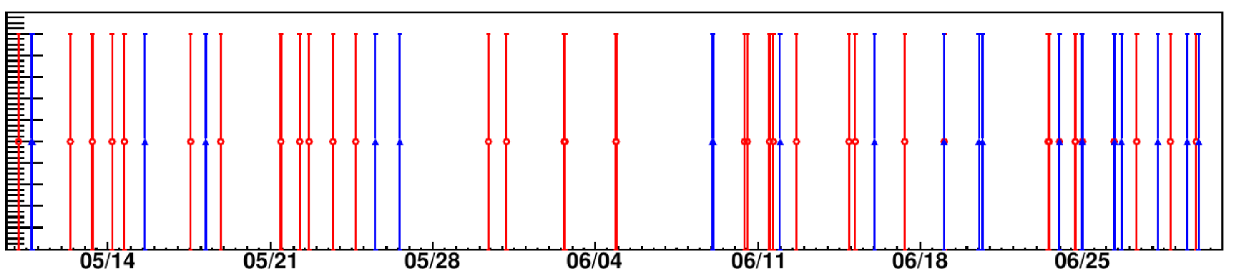
The CDC FEE uses the Xilinx SEU mitigation logic to correct the configuration memory altered by SEU. Successful SEU correction occurs a few times a day without affecting the data acquisition, and it is monitored through the TTD system. However, the SEU mitigation code is not able to correct multiple bit errors at a time or errors in the mitigation code itself. It does not correct the data memory either, including those used as a part of state machines. These unrecoverable errors occurred at an average rate of once per day, 40% of which were detected by the SEU mitigation logic, as shown in Fig. 7. Then the FPGA has to be reprogrammed; the reprogramming takes less than 10 s, but the detection and identification procedure of the error currently takes a much longer time, typically more than 5 minutes.
The TOP FEE also uses the SEU mitigation logic from Xilinx, and ARICH uses a custom SEU mitigation logic [13] which has a superior performance compared with the one provided by Xilinx for the Spartan-6 FPGA.
Reduction of the down time is foreseen by automating the reprogramming procedure of the unrecoverable SEU errors.
IV-B Link Errors
Both custom protocols, b2tt and Belle2link, use predefined 8b10b control symbols to define the protocol and have an embedded data error checking mechanism using a cyclic redundancy check (CRC). An incorrect control symbol and a CRC error are identified as a link error, and propagated to the TTD system to stop the run. The link error, either in b2tt or Belle2link, has been so far the most frequent cause that stopped data taking. The error often repeated from the same link, caused by a particular version of firmware which happened to be more timing critical, on the line that has a smaller margin. Unstable FEE boards and cables were replaced to avoid the weak links during the shutdown period to make the entire system more stable.
We have made an investigation of the electric characteristics of the signal running on the CAT7 cables from the FTSW to the FEE during the summer shutdown period of 2020. We identified two particular cases that were improved during summer, one for KLM and the other for CDC.
For KLM, we find a large sine-wave noise of around 300 kHz on the category-7 cables. This turned out to be due to the lack of a proper ground connection at the FEE, and the 20 m long category-7 cables between FTSW and FEE. We have moved the location of the FTSW modules by introducing new small VMEbus crates and reducing the cable length to 10 m, and installed a proper grounding connection at the FEE. Some of the LVDS drivers of the KLM FEE were damaged and were replaced during the run in 2020; the improper ground connection is suspected to have induced a large current from an external noise causing the damage.
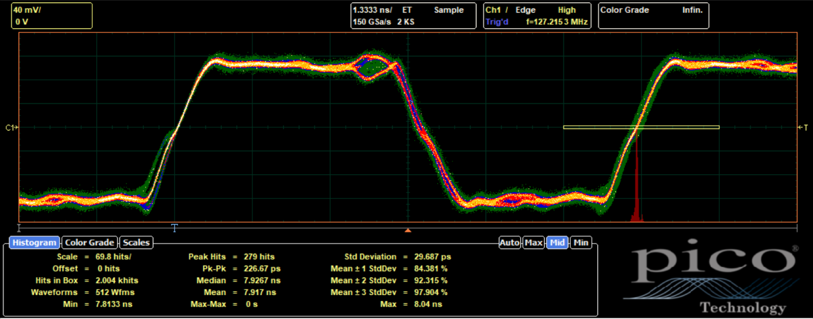
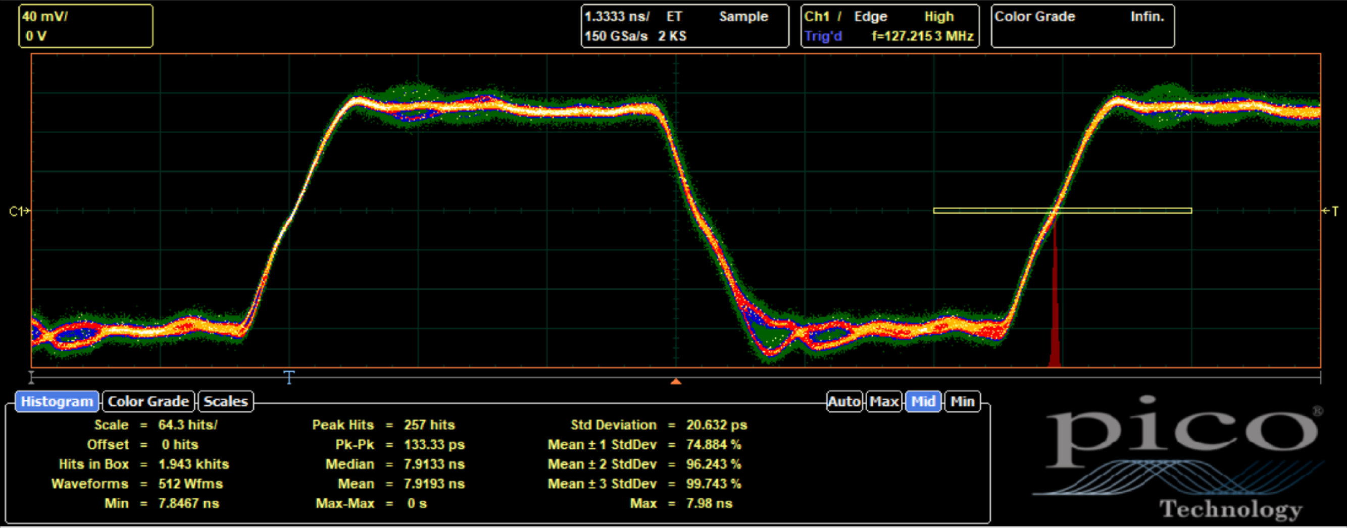
The CDC FEE boards were not accessible during the summer shutdown of 2020, but the clock and serial signals were examined near the FTSW module. We found a combination of a lower FTSW driver amplitude and a higher current draw at the FEE in particular connections makes it less immune to the crosstalk from the serial-b2tt-encoded line to the clock line. The crosstalk causes a glitch in the clock and causes a data error in Belle2link, although the glitch is not large enough to cause an error in the phase lock loop (PLL). Mostly due to this problem, up to 10 out of 299 FEE boards were masked in the worst case. This problem was completely cured by adding a delay to the serial link output of the FPGA firmware, to avoid the edge transition of the serial b2tt data near the clock edge as shown in Fig. 8.
IV-C Hardware Failures, Other Problems, and Prospects
The largest down time occurred during the run was due to the failure in one of the KLM FEE boards. This FEE was a data concentrator and could not be masked without losing a large fraction of data. The module had to be replaced by stopping the beam and accessing the detector area. Other hardware failures of the FEE boards for TOP and ARICH occurred inside the detector and it will not be possible to replace them until the long shutdown period in 2022.
There was also down time due to the COPPER backend system, the HLT system, and slow control software problems.
The down time of the data acquisition system is one of the major concerns of the future run period of Belle II. We have improved the stability of the system in various ways at every major shutdown period and also during the run period. For the unavoidable errors such as the single event upset of the FEE, we are improving the monitor and error recovery procedure [14].
V Conclusions
We have presented the performance of the unified readout system of the Belle II experiment at the SuperKEKB collider during the first two years of the operation. We have been smoothly running at about 4 kHz level-1 trigger rate with a readout dead-time fraction below 1%. The largest dead time is from the unavoidable continuous injection veto, but a similarly large fraction of the dead time was caused by various errors in the unified readout system as well as in the rest of the data acquisition system. We have described the major problems we encountered, and solutions we found to improve the stability of the system and to reduce the dead time. We also confirmed using the real data that the unified readout system can handle the design level-1 trigger rate of 30 kHz. We expect a more stable operation with a higher luminosity and trigger rate in the coming runs.
References
- [1] T. Abe et al. (Belle II Collaboration), “Belle II Technical Design Report,” arXiv:1011.0352 [physics.ins-det].
- [2] K. Akai, K. Furukawa, H. Koiso et al. (SuperKEKB Collaboration), “SuperKEKB collider,” Nucl. Instrum. Methods Phys. Res., Sect. A vol. 907, pp. 188–199, Nov. 2018, 10.1016/j.nima.2018.08.017.
- [3] M. Nakao, T. Higuchi, R. Itoh, S.Y. Suzuki, “Data Acquisition System for Belle II,” J. Instrum., vol. 5, C12004, Dec. 2010, 10.1088/1748-0221/5/12/C12004.
- [4] S. Yamada, R. Itoh, T. Konno, Z. Liu, M. Nakao, S. Y. Suzuki, J. Zhao, “Common Readout Subsystem for the Belle II Experiment and Its Performance Measurement,” IEEE Trans. Nucl. Sci., vol. 64, pp. 1415–1419, Apr. 2017, 10.1109/TNS.2017.2693297.
- [5] M. Nakao, “Timing Distribution for the Belle II Data Acquisition System,” J. Instrum., vol. 7, C01028, Jan. 2012, 10.1088/1748-0221/7/01/C01028.
- [6] VITA Standards, ANSI/VITA 1.0-1994. [Online] Available: https://www.vita.com/Standards.
- [7] Xilinx. [Online] Available: https://www.xilinx.com/.
- [8] “1149.7-2009 - IEEE Standard for Reduced-Pin and Enhanced-Functionality Test Access Port and Boundary-Scan Architecture,” Feb. 2010, 10.1109/IEEESTD.2010.5412866.
- [9] D. Sun, Z. Liu, J. Zhao, H. Xu, “Belle2Link: a Global data Readout and Transmission for Belle II Experiment at KEK,” Phys. Procedia, vol. 37, pp. 1933–1939, Oct. 2012, 10.1016/j.phpro.2012.01.036
- [10] M. Andrew, “128 channel waveform sampling digitizer/readout in the TOP counter for the Belle II upgrade,” PoS(TIPP2014), 171, 10.22323/1.213.0171.
- [11] Intel FPGAs and Programmable Devices. [Online] Available: https://www.intel.com/content/www/us/en/products/programmable.html
- [12] T. Higuchi, M. Nakao, E. Nakano, “Radiation Tolerance of Readout Electronics for Belle II,” J. Instrum., 7, C01028, Feb. 2012, 10.1088/1748-0221/7/02/C02022.
- [13] R. Giordano, Y. Lai, S. Korpar, R. Pestotnik, A. Lozar, L. Šantelj, M. Shoji, S. Nishida, “Intermodular Configuration Scrubbing of On-detector FPGAs for the ARICH at Belle II,” 22nd Virtual IEEE Real Time Conference, Oct. 12–23, 2020.
- [14] T. Kunigo, A. Baur, M. Prim, S. Y. Suzuki, M. Nakao, R. Itoh, S. Yamada, Q.D. Zhou, R. Sugiura “Real-time monitoring of operational data in the Belle II experiment,” 22nd Virtual IEEE Real Time Conference, Oct. 12–23, 2020.